 Open Access Article
Generation of mode-locked pulses based on D-shaped fiber with CdTe as a saturable absorber in the C-band region
Harith Ahmad *ab,
Nur Hidayah Mansora,
Siti Aiyah Reduana and
Rizal Ramlia
aPhotonics Research Center, University of Malaya, 50603 Kuala Lumpur, Malaysia. E-mail: harith@um.edu.my
bDepartment of Physics, Faculty of Science, Universiti Malaya, 50603 Kuala Lumpur, Malaysia
First published on 18th March 2022
Abstract
This study demonstrates the potential of cadmium telluride (CdTe), a part of the quantum dot (QD) family, as a saturable absorber (SA) to generate ultrashort pulses at the C-band region. The SA was fabricated by drop-casting the CdTe material onto the exposed core of the D-shaped fiber. The nonlinear property of the fabricated SA has a modulation depth of 1.87% and saturation intensity of 6.0 kW cm−2. The mode-locked laser was generated after the SA was integrated into the erbium-doped fiber laser (EDFL) cavity at a threshold pump power of 192.1 mW giving a center wavelength of 1559 nm and a pulse duration of 770 fs. The maximum average output and peak power were measured to be 2.8 mW and 0.208 kW, respectively. The mode-locked fiber laser generated a signal-to-noise ratio (SNR) of 67.7 dB, proving that the generated mode-locked pulses were very stable. The current work indicates that the novel CdTe device can provide stable mode-locked lasers in the C-band region.
Introduction
Theodore Maiman demonstrated the first demonstration of the laser in 1960 at the Hughes Research Laboratories.1 Later, optical fiber was discovered by Kao and Hockham2 in 1966 providing inroads for the development of optical fiber devices. Consequently, significant progress in the field of optical amplifiers in the region of S- to L-bands3–12 as well as the development of multiwavelength fiber lasers13–22 and also optical sensor devices23–25 has taken place. As technology grew, new industrial demands for high-power lasers as an alternative to the bulk and complex laser systems in the area of gas spectroscopy, medicine, and manufacturing have been the main focus of laser research.26–31 At the same time, there has been an intense development of ultrafast fiber lasers due to the favourable properties of the laser outputs, such as short pulse width, high-intensity pulses, and broad supercontinuum outputs.32–34 A mode-locked laser can be generated based on active or passive techniques. The former approach was expensive and occupied larger space. The latter was a better alternative to overcome these challenges, demonstrating the relative advantages of simple design, alignment-free, and lower cost.35–39 One of the common approaches is using saturable absorbers (SAs), which convert continuous wave (CW) output into a pulse train of short pulses through light–matter interactions based on the self-amplitude modulation of light inside the laser cavity.40–42 SAs can be classified as artificial or real.Artificial SA, such as nonlinear polarization rotation, Kerr-lensing, and nonlinear fiber loop mirror, demonstrates a high pulse intensity with low insertion loss when introduced into the laser cavity.43–46 For example, in the real SAs, SESAM has been proven many years back to be an effective material in generating ultrashort pulses in optical fiber lasers but has the disadvantages of being expensive, complex, and with only a narrow bandwidth operation.47–50 Therefore, to seek new and high-performance SA, there is a need to explore other materials, especially nanomaterials, for instance, carbon nanotubes (CNT) and graphene.51 CNT as an SA has a superior performance in inducing mode-locking and broadband operation. The drawbacks of CNT are due to nanotubes agglomeration and large nanotubes energy distribution that will produce a high non-saturable loss in the laser cavity.51 Meanwhile, graphene can create a short pulse duration over a broad bandwidth.47 Some graphene derivatives, such as graphene oxide and reduced graphene oxide, promise great performance characteristics in tunability and wideband mode-locked operation.52 However, there has been a slight drawback with these materials when used as thin-film SAs, which when introduced into the laser cavity experience a low optical damage threshold.53 This is due to the direct exposure of the materials with the propagating beam strongly causing them to be easily damaged. Consequently, numerous research approaches were made using different nanomaterials, such as transition metal dichalcogenide (TMD)54 and black phosphorus.55
Another interesting material is cadmium telluride (CdTe), a material compound with potential uses in many applications, including solar cells,56 photovoltaic devices,57 and biological applications.58 This is due to its energy band gap value and optical properties, allowing conversion from sunlight to electric energy efficiently.59 It has been reported that CdTe can absorb about 92% of visible light in the thickness of 1 μm, which implies that CdTe has a high optical absorption coefficient of about 104 cm−1.59–61 CdTe is also suitable for photovoltaic solar cells due to its direct bandgap (1.44 eV), near the optimum for photovoltaic solar energy conversion.62 However, there are only a few reports on using CdTe for generating pulsed outputs in fiber laser systems. Rosol et al.63 proposed a Q-switching laser in an EDFL cavity using cadmium selenide deposited onto poly-methyl methacrylate (PMMA) microfiber. The Q-switched laser had a repetition rate of 37 kHz to 64 kHz at the pump power range of 34.0 mW to 74.0 mW.63 The result shows the suitability of CdTe to be explored in the generation of ultrashort pulses in optical fiber lasers. Hence, CdTe, can be of interest to explore the generation of ultrashort pulses in optical fiber lasers.
Saturable absorbers (SAs) can be fabricated by utilizing various techniques, including composites with polymer to generate thin films and material deposition directly onto D-shaped fiber51 or microfiber.64 The approach of composite materials, which uses a polymer as the host material, can be efficient; however, the thin film form has a lower damage threshold and power tolerance.51 To circumvent this constraint, D-shaped fibers and microfibers coated with materials would have a better damage threshold, applicable to generating a high power output from fiber laser systems.64,65 In the case of tapered microfibers, such as those drawn using the flame brushing technique, a tapered zone would be created in all directions over the diameter of the fiber. It would substantially lower the tapered waist, resulting in higher transmission loss due to the removal of the cladding region. For the D-shaped fiber, only one side of the diameter of the fiber is being polished or removed, leaving the other side intact. As a result, the waist diameter would be larger than the tapered microfibers, resulting in a lower signal loss.65 Furthermore, the environment can affect the microfiber performance, which might impair their performance.64 This work used the coated D-shaped fiber with CdTe to generate the mode-locked pulses.
The mode-locked laser produced a center wavelength, pulse width, and signal-to-noise ratio (SNR) of 1559 nm, 770 fs, and 67.7 dB, respectively, at an initial pump power of 192.1 mW. At a maximum pump power of 510 mW, the maximum average output and peak powers were 2.8 mW and 0.208 kW, respectively. A passive mode-locking approach has promising applications in various industries, such as optoelectronics, photovoltaics, and medicine,66–68 due to the high-quality beam, ease of production, and cost-effective system47 with the opportunity of generating short pulses with high peak power.34
Fabrication and characterization of CdTe
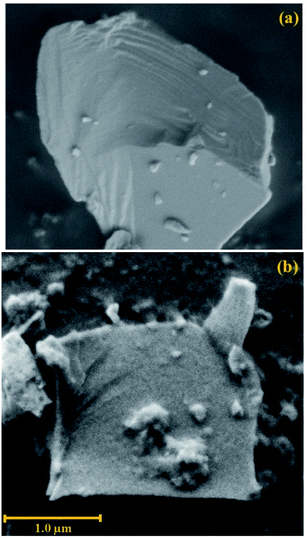
Initially, 100 mg of CdTe powder (powder, <250 μm, deposition grade, ≥99.98% trace metals basis, Sigma Aldrich) was added to a glass beaker filled with 10 mL of isopropyl alcohol (IPA, ≥99.7%, Sigma Aldrich) solution. The mixture was sonicated for 3 hours to attain a homogenous solution of CdTe. Subsequently, the obtained black suspension was transferred into a centrifuge tube and subjected to centrifugation at 4000 rpm for 10 minutes. This centrifugation process separated the residual unexfoliated CdTe powder from the CdTe solution. After centrifugation, the supernatant was collected. The black supernatant containing the exfoliated CdTe flakes was transferred into a glass vial and labeled as the exfoliated CdTe solution. 5 μL of exfoliated CdTe solution was used to coat onto the surface of the polished fiber and further used as an SA in this work.The field emission scanning electron microscope (FESEM, Hitachi SU8220), working at 2.0 kV, was utilized to examine the surface morphology of CdTe in the bulk form as well as after the post-exfoliation process. Fig. 1 shows FESEM images of bulk and exfoliated CdTe captured at the same magnification (at 300![[thin space (1/6-em)]](https://www.rsc.org/images/entities/char_2009.gif) 00× magnification). As shown in Fig. 1(a), the FESEM image of bulk CdTe demonstrated that CdTe is composed of multiple closely stacked layers, forming the 3D bulk structure grain. The grains exhibited an average size of about 2.5 μm. Due to the weak van der Waals' bonding between layers, the bulk CdTe experienced an exfoliation upon the sonication process to produce a few layers of CdTe. As shown in Fig. 1(b), the formation of a thin flake of CdTe revealed the success of the exfoliation of CdTe using the ultrasonication-assisted approach. It can be observed that the exfoliated CdTe displayed a flake-like structure with an irregular shape and lateral dimension of approximately 2.0 μm.
00× magnification). As shown in Fig. 1(a), the FESEM image of bulk CdTe demonstrated that CdTe is composed of multiple closely stacked layers, forming the 3D bulk structure grain. The grains exhibited an average size of about 2.5 μm. Due to the weak van der Waals' bonding between layers, the bulk CdTe experienced an exfoliation upon the sonication process to produce a few layers of CdTe. As shown in Fig. 1(b), the formation of a thin flake of CdTe revealed the success of the exfoliation of CdTe using the ultrasonication-assisted approach. It can be observed that the exfoliated CdTe displayed a flake-like structure with an irregular shape and lateral dimension of approximately 2.0 μm.
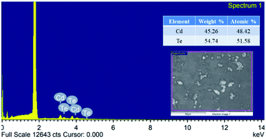
Fig. 2 shows the EDX spectrum of the exfoliated CdTe's scanned area after being drop cast onto a silicon (Si) substrate (as shown in the inserted image). It was evident that the primary constituent elements of CdTe were cadmium (Cd) and tellurium (Te), as the signal peaks representing both elements as observed in the EDX spectrum. The quantification of the signal peak indicated that the atomic percentages of Cd and Te elements were measured to be 48.42% and 51.48%, respectively, thus giving an atomic ratio of 0.94![[thin space (1/6-em)]](https://www.rsc.org/images/entities/char_2009.gif) :
:![[thin space (1/6-em)]](https://www.rsc.org/images/entities/char_2009.gif) 1. This result is nearly similar to the stoichiometry of CdTe that is 1
1. This result is nearly similar to the stoichiometry of CdTe that is 1![[thin space (1/6-em)]](https://www.rsc.org/images/entities/char_2009.gif) :
:![[thin space (1/6-em)]](https://www.rsc.org/images/entities/char_2009.gif) 1. The intense signal located at about 1.8 eV referred to the silicon (Si) element, which is due to the use of a Si wafer to hold the sample.
1. The intense signal located at about 1.8 eV referred to the silicon (Si) element, which is due to the use of a Si wafer to hold the sample.
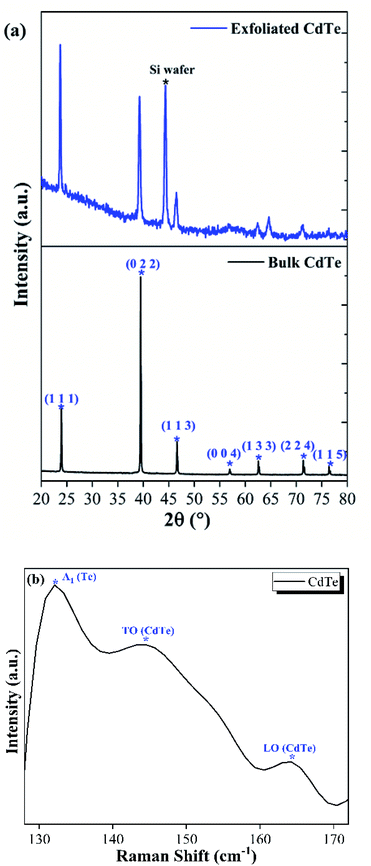
The X-ray diffraction analysis was performed using a PANalytical Empyrean X-ray diffractometer (XRD) with Cu-Kα radiation (λ = 1.540 Å) for bulk CdTe powder, and Rigaku Smartlab X-ray diffractometer (XRD) for exfoliated CdTe deposited onto a silicon substrate. It was done to determine the crystallographic structure of bulk and exfoliated CdTe. Based on the XRD spectrum presented in Fig. 3(a), a few sharp diffraction peaks are observed at 2θ = 23.9, 39.5, 46.6, 56.9, 62.6, 71.4, and 76.4°. These diffraction peaks match well with the (1 1 1), (0 2 2), (1 1 3), (0 0 4), (1 3 3), (2 2 4), and (1 1 5) planes of cubic CdTe, respectively, as indexed in the joint committee on powder diffraction standards (JCPDS) file with the reference number of 98-010-8238. Thus, the appearance of sharp and well-defined peaks elucidated the highly crystalline structure of bulk CdTe. Moreover, no other diffraction peaks of impurities were found in the XRD pattern, hence, indicating the high purity of bulk CdTe. After the exfoliation process, the diffraction peaks became slightly broadened and a new peak centered at 44.5 ° was observed, which can be assigned to the (2 2 0) plane of silicon (Si).69 The slightly broad and the reduction in the intensity of (0 2 2) diffraction peak confirms the exfoliation of CdTe had occurred.
A Renishaw inVia Raman microscope with a laser excitation wavelength at 514 nm was used to record the Raman spectra of CdTe. As in Fig. 3(b), three peaks appeared at 132, 144, and 164 cm−1, which are the Raman characteristic peaks of CdTe.70 The peak at 132 cm−1 corresponds to the A1 Raman vibrational mode of tellurium (Te).71 The peaks at 144 cm−1 and 164 cm−1 can be assigned to the transverse-optic (TO) and the longitudinal-optic (LO) phonon modes of CdTe, respectively.59
The surface profile measurement was conducted using a DEKTAK 150 surface profiler to measure the thickness of the exfoliated CdTe. Initially, the CdTe solution was spin-coated on the glass substrate and left to dry under the ambient conditions before conducting the measurements. As a result, the thickness of the exfoliated CdTe was measured to be about 88 nm.
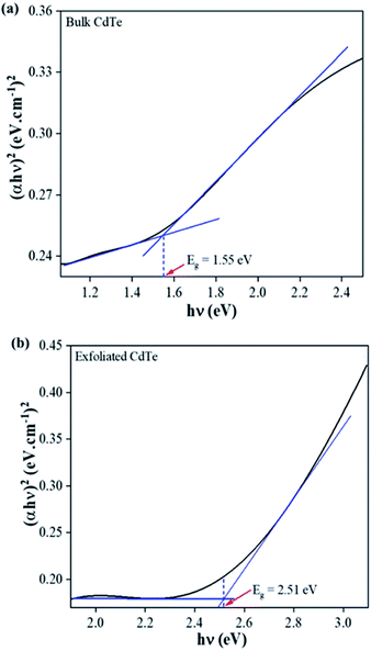
To measure the energy bandgap (Eg) of bulk and exfoliated CdTe, the Tauc plot was extracted from the UV-visible-near infrared (UV-vis-NIR) absorption spectrum recorded using a PerkinElmer Lambda 750 UV-vis-NIR spectrometer and fitted according to the standard Tauc's relation of αhv = A(hv − Eg)n. In this relation, α, hv, A, and Eg correspond to the optical absorption coefficient, incident photon energy, proportion constant, and optical energy band gap. Here, n takes the value of  to indicate that both bulk and exfoliated CdTe exhibit the allowed optical transition responsible for absorption. In, the Tauc's plots of (αhv)2 versus hv were plotted for bulk and exfoliated CdTe, as presented in Fig. 4(a) and (b), respectively. From the Tauc plot, the bulk and exfoliated CdTe band gap were extracted as the intercept of the linear fit with the x-axis (αhv)2 = 0, giving the value of approximately 1.55 eV and 2.51 eV, respectively.
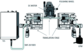
The wheel polishing method is used to fabricate the D-shaped fiber to obtain a smooth polished surface.52,72 Two Newport M-562-DX-Y-Z alignment stages with Newport 561-FH fiber holders were utilized to fix the single-mode fiber (SMF-28). The core diameter of the SMF-28 was 9 μm and had a numerical aperture of 125 μm. The SMF-28 was spliced into two fiber pigtails on both ends. About 5 cm of the polymer jacket was stripped out from the SMF-28 optical fiber to expose the bare sections directly to the polishing wheel. The polishing wheel was positioned on a Newport M-562 X-Y alignment stage for ease of movement, horizontally and vertically. The input power was then supplied to a 6 V DC motor of the polishing wheel. Silicon carbide paper with a diameter of 13 mm and a grit size of 400 was wrapped around the polishing wheel. The motor rotating the polishing wheel exhibited a maximum speed of 11![[thin space (1/6-em)]](https://www.rsc.org/images/entities/char_2009.gif) 442 rpm with a torque of 1.04 × 10⁻³ Nm. The experimental setup for the wheel-polishing technique is shown in Fig. 5.
442 rpm with a torque of 1.04 × 10⁻³ Nm. The experimental setup for the wheel-polishing technique is shown in Fig. 5.
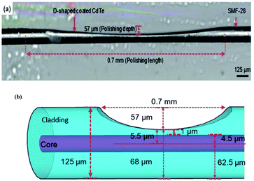
The polishing wheel should not be in contact with the bare region of the SMF-28 in the early stages because friction between the silicon carbide surface and the SMF-28 will produce a significant force that could cause the SMF-28 to break, thereby damaging the polishing equipment. Alternatively, the polishing wheel had to be spun until it reached its optimal speed before being carefully elevated to the bare SMF-28. For monitoring purposes, each of the spliced pigtails was connected to a tunable laser source (TLS) and an optical power meter (OPM). The TLS will emit a signal at 1550 nm into the SMF-28 optical fiber at an optical power of 13 dBm. Optical power loss was measured constantly throughout the polishing process until an insertion loss of 3 dB was reached, as shown in Fig. 6(a) with a polishing depth of around 57 μm. Then, the motor stopped, and the D-shaped fiber was cautiously transferred onto a clean glass slide. The D-shaped fiber was cleaned using an alcohol solution to remove any debris produced during the polishing process. Few drops of CdTe were deposited onto the D-shaped fiber.
Fig. 6(a) shows the microscopic image of the fabricated D-shaped fiber at 100×-magnification with a scale bar obtained using an Olympus BX53M optical microscope with calibrated ToupView software by the manufacturer. Normally a single-mode fiber (SMF-28) would have a dimension of cladding and core diameters of 125 and 9 μm, respectively. Therefore, the cladding radius from the center of the core is 62.5 μm. As in Fig. 6(b), the polishing wheel only cuts at one side of the fiber, which is the upper part in the figure. Therefore, about 57.0 μm of the cladding was removed, giving only about 1 μm from the edge of the core. As such, at the necking region, the part with the smallest diameter would have a dimension of 4.5 (core radius) plus 1 μm of the cladding, giving a total radius of 5.5 μm. The radius at the bottom part of the figure remains the same at 62.5 μm.
The balanced twin-detector technique was used to determine the nonlinear optical absorption of CdTe deposited onto the D-shaped fiber. A graph of normalized absorption again pump power intensity was plotted as shown in Fig. 7(a). A commercial ELMO femtosecond laser was used with a central wavelength of 1560 nm, a repetition rate of 100 MHz, and a pulse duration of 150 fs. The light was divided equally using a 50![[thin space (1/6-em)]](https://www.rsc.org/images/entities/char_2009.gif) :
:![[thin space (1/6-em)]](https://www.rsc.org/images/entities/char_2009.gif) 50 coupler where one was used for reference while the other was connected to the fabricated SA. The input power was continuously adjusted using the attenuator, after which the resulting change in output power was recorded as given in Fig. 7(a). The saturation model equation was used to fit the measured data as shown below:
50 coupler where one was used for reference while the other was connected to the fabricated SA. The input power was continuously adjusted using the attenuator, after which the resulting change in output power was recorded as given in Fig. 7(a). The saturation model equation was used to fit the measured data as shown below:
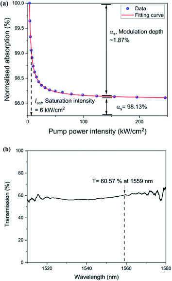 | ||
| Fig. 7 (a) Nonlinear optical absorption of D-shaped fiber coated with CdTe (b) Linear transmission curve spectrum of the SA. | ||
To observe the distribution of CdTe on the surface of the polished fiber, the field emission scanning electron microscopy (FESEM) characterization was performed using a JEOL JSM 7600-F FESEM operated at 1.0 kV of accelerating voltage. The FESEM images were taken at 15×, 50×, and 500× magnification, as shown in Fig. 8(a)–(c), respectively. Fig. 8(a) shows the FESEM image of the polished fiber coated with CdTe obtained under low magnification. After zooming in at the polished area up to 50× magnification (Fig. 8(b)), a slightly uneven texture was observed along the surface of the polished area with a random distribution. A magnification of 500× was performed as shown in Fig. 8(c) to get a better picture. The obtained results revealed that the distribution of CdTe onto the fiber surfaces was not uniform; however, most of the polished surface area was coated with CdTe flakes of various sizes and thicknesses. It is worth noting that the distortion of the FESEM image was due to the charging effect that occurred during the secondary electron FESEM analysis as the surface was not coated with gold, which can also be observed as bright regions.
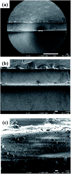 | ||
| Fig. 8 FESEM images of CdTe deposited onto the surface of polished fiber captured at (a) 15×, (b) 50×, and (c) 500× magnification. | ||
Experimental setup
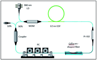
Fig. 9 shows the configuration of the erbium-doped fiber (EDF) cavity used in this work. A 980 nm laser diode (LD) was used to pump the EDF, which was connected to a 980/1550 nm wavelength division multiplexer (WDM). The common port of the WDM was connected to 0.5 m EDF, which represented the cavity's linear gain medium. The EDF used was Er-110-4/125 (Liekki), which has a numerical aperture (NA) of 0.2, a mode field diameter of 6.5 μm, and an absorption coefficient of 110 dB m−1 at 1530 nm. First, an insensitive polarization isolator (PI-ISO) was placed after the gain medium to ensure that the signal propagated in the cavity in a clockwise direction. Next, the fabricated CdTe-coated D-shaped-based SA was placed at the output end of the PI-ISO, which was then connected to a polarization controller (PC). The fabricated CdTe-coated D-shaped based SA was placed at the output of the ISO, which was in turn connected to a polarization controller (PC). The signal was then connected to a 90![[thin space (1/6-em)]](https://www.rsc.org/images/entities/char_2009.gif) :
:![[thin space (1/6-em)]](https://www.rsc.org/images/entities/char_2009.gif) 10 optical coupler (OC), with the 90% port attached to the 1550 nm port of WDM, completing the fiber laser cavity. To measure the optical and temporal characteristics of the output, a 10% port of the OC was used to extract a portion of the signal.
10 optical coupler (OC), with the 90% port attached to the 1550 nm port of WDM, completing the fiber laser cavity. To measure the optical and temporal characteristics of the output, a 10% port of the OC was used to extract a portion of the signal.
The total length of this configuration was about 11.77 m, consisting of 11.27 m of single-mode fibers (SMF-28s) and 0.5 m of the EDF. The group velocity dispersion (GVD) was calculated using the equation GVD = −λDλ/2πc, whereby Dλ is the material dispersion, λ is the operating wavelength, and c is the speed of light. For the EDF, the material dispersion was −17.57 ps nm−1 km−1, giving a GVDEDF of 0.0227 ps2 m−1, while the material dispersion for the SMF-28 s was 16.65 ps nm−1 km−1, giving a GVDSMF of −0.0215 ps2 m−1. The total net cavity dispersion of the cavity was calculated to be −0.23 ps2 using the formula of GVDcavity = LEDFGVDEDF + LSMFGVDSMF, with LEDF and LSMF being the length for the EDF and SMF-28, respectively. This indicates that the EDF mode-locked laser was operating in the anomalous dispersion regime.
Results and discussion
At a threshold pump power of 39.8 mW, a continuous wave (CW) was generated. Upon incorporating the CdTe D-shaped fiber inside the cavity, fundamental mode-locked pulses appeared at 192.1 mW. Fig. 10 shows the presence of Kelly's sidebands on both sides of the optical spectrum measured using the Yokogawa AQ6370B optical spectrum analyzer (OSA), which indicates that the mode-locked laser was operating in the anomalous dispersion regime. The optical spectrum had 3 dB bandwidth of 4 nm with a center wavelength of 1559 nm, enlarged in the inset of Fig. 10.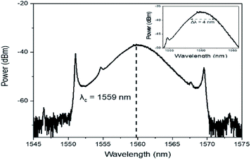 | ||
| Fig. 10 Output spectrum characteristics of mode-locked EDFL using CdTe SA (inset shows the enlarged optical spectrum to show the FWHM). | ||
Using a Yokogawa DLM2054 oscilloscope (OSC), a pulse train with an interval between the adjacent pulses of 56.89 ns was measured from the generated mode-locked pulses, as shown in Fig. 11(a). This agreed well with the cavity round trip time with a fundamental repetition rate of 17.6 MHz. Fig. 11(b) shows the autocorrelation (AC) trace with a red line fit, giving a full width at half maximum (FWHM) of ∼1.19 ps. By taking the deconvolution factor of sech2 into consideration, which is 0.648, the actual pulse width would be ∼0.77 ps. The time-bandwidth product (TBP) can be computed using the formula of  , where the Δλ is the 3 dB bandwidth, Δτ is the minimum pulse width, c is the speed of light and λ is the center wavelength. The TBP was calculated to be 0.38, slightly larger than the theoretical transform-limited value of 0.315, indicating that the pulses are slightly chirped.
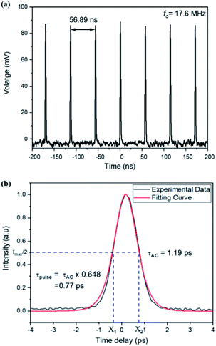 | ||
| Fig. 11 Output characteristics of mode-locked EDFL showing (a) output pulse train and (b) pulse width of a single mode-locked pulse. | ||
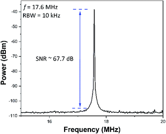
Fig. 12 shows the radiofrequency (RF) spectrum obtained using the Rohde & Schwarz FPC1000 radio-frequency spectrum analyzer (RFSA) paired with a 12.5 GHz Newport 818-BB-35F photodetector, indicating a signal-to-noise ratio (SNR) of 67.7 dB at the fundamental repetition rate of 17.6 MHz. Consequently, a stable mode-locked operation was obtained using a D-shaped fiber coated with CdTe.
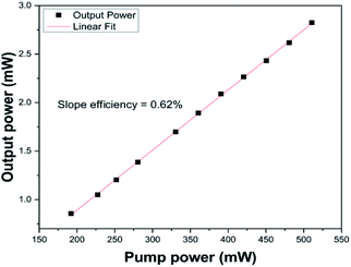
A linear line graph of average output power against pump power was plotted, as shown in Fig. 13. The mode-locked laser was operated at the fundamental mode throughout the pump power range of 192.10 to 510.75 mW with a slope efficiency of 0.62%. The graph shows a positive gradient with a linear relationship between the average output power and pump power. For example, the average output power increased from 0.86 to 2.82 mW when the pump power increased from 192.1 to 510.75 mW. The maximum average output power, pulse energy, and peak power obtained from the mode-locked laser were 2.82 mW, 0.16 nJ, and 0.208 kW, respectively.
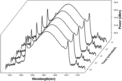
The stability test of the mode-locked output was performed at a fixed pump power of 280.5 mW. The output spectrum was examined for 50 minutes. Fig. 14 shows a spectrum obtained over 50 minutes in 10 minutes intervals. There are no noticeable changes in the spectrum's shape or shift in the center wavelength of 1559 nm throughout the observation, indicating a stable mode-locked laser operation.
Table 1 shows the comparison between the performance of the mode-locked pulses generated in this work with that from other works using different SAs with a particular focus on modulation depth and net cavity dispersion. In this work, the modulation depth obtained was 1.87% in comparison with other results ranging from 32.4% to 0.63%, for the case of MgO and MoSe2 saturable absorbers. This indicates that the modulation depth value was in between these values, as given in Table 1. As for the performance of the mode-locked pulses, the result of the current work showed that the generated center wavelength, 1559 nm, was comparable with that from other studies in the C-band region with the wavelength output of our result was slightly lower than that reported in ref. 51, 73, 74, 75, 76 and 77 but longer than those reported in ref. 78, 79 and 80. The repetition rate generated by this work was 17.6 MHz, which was more significant than that from most previous works but slightly lower than that reported in ref. 74 and 79. The repetition rate value depended on the cavity length, which can be tuned by different lengths of SMF and the gain medium inserted in the cavity. The SNR generated in this work was 67.7 dB. It is the highest SNR value compared to Mo2C,73 graphite,51 MoS2,74 MoTe2,75 PdS2,76 MoSe2,78 MgO,77 Mxene (Ti3C2Tx)79 and SnSe2,80 which clearly indicate that this system is very stable. The pulse width generated using CdTe deposited on D-shaped fiber in this work was 0.77 ps, which was shorter compared to most of those reported in the selected literature studies presented in Table 1. It is worth noting that few reported works51,73,74 generated lower pulse widths. This could be due to the lower net cavity dispersion. It was suggested that a predicted shorter pulse width value could be generated by CdTe-deposited D-shaped fiber with a lower net cavity anomalous dispersion moving toward zero dispersions by manipulating the cavity length.81 It was further confirmed by Zhang et al.,82 who simulated that when the anomalous dispersion value decreased, the pulse width value also decreased proportionally. Thus, the dispersion in the cavity could be controlled by the lengths of single-mode fiber and gain medium used. Further demonstration of intracavity dispersion management generating shorter pulse width was observed using, MoTe2,75 MgO (ref. 77) and SnSe2.80 The net cavity dispersion of this work is comparatively similar to that of PdS2,76 MoSe2![[thin space (1/6-em)]](https://www.rsc.org/images/entities/char_2009.gif) 78 and Mxene (Ti3C2Tx),79 with the values of −0.23 ps2 against −0.21 ps2, −0.22 ps2 and −0.14 ps2, respectively. Our results on pulse width and SNR are comparatively better than those reported in the above-mentioned works, which could be due to larger modulation depth value generating shorter pulse width typically reported by Jeon.81 Conversely, Feng et al.79 reported that a larger modulation depth value compared to that from our work, which generated a pulse width of 0.98 ps. Based on Table 1, we can see that majority of the works use the drop casting method mainly because of its simplicity. From the findings of this work, it demonstrated that CdTe deposited on D-shaped fiber could generate efficient and high-performance pulse-fiber lasers based on the high repetition rate, short pulse width and high SNR value.
78 and Mxene (Ti3C2Tx),79 with the values of −0.23 ps2 against −0.21 ps2, −0.22 ps2 and −0.14 ps2, respectively. Our results on pulse width and SNR are comparatively better than those reported in the above-mentioned works, which could be due to larger modulation depth value generating shorter pulse width typically reported by Jeon.81 Conversely, Feng et al.79 reported that a larger modulation depth value compared to that from our work, which generated a pulse width of 0.98 ps. Based on Table 1, we can see that majority of the works use the drop casting method mainly because of its simplicity. From the findings of this work, it demonstrated that CdTe deposited on D-shaped fiber could generate efficient and high-performance pulse-fiber lasers based on the high repetition rate, short pulse width and high SNR value.
| Material | Coating method | Modulation depth (%) | Center wavelength (nm) | Pulse width (ps) | Repetition rate (MHz) | SNR (dB) | Net cavity dispersion (ps2) | Ref. |
|---|---|---|---|---|---|---|---|---|
| Mo2C | Drop-casting | 5.1 | 1561.6 | 0.29 | 7.9 | 61.0 | −0.12 | 73 |
| Graphite | Film attachment | 3.3 | 1565.0 | 0.22 | 15.7 | 63.0 | −0.087 | 51 |
| MoS2 | Film attachment | 2.5 | 1568.0 | 0.63 | 26.0 | 61.0 | −0.041 | 74 |
| MoTe2 | Drop-casting | 1.8 | 1561.0 | 1.20 | 5.2 | 50.0 | −0.58 | 75 |
| PdS2 | Drop-casting | 1.7 | 1565.8 | 0.80 | 12.1 | 61.0 | −0.21 | 76 |
| MoSe2 | Sandwich | 0.63 | 1558 | 1.76 | 8.028 | 61.5 | −0.22 | 77 |
| MgO | Sandwich | 32.4 | 1569.1 | 5.6 | 3.5 | 50 | −1.17 | 78 |
| MXene (Ti3C2TX) | Drop-casting | 10.3 | 1530.4 | 0.98 | 27.9 | 54.6 | −0.14 | 79 |
| SnSe2 | Drop-casting | 6.38 | 1530 | 1.089 | 8.3 | 53 | −0.56 | 80 |
| CdTe | Drop-casting | 1.87 | 1559.0 | 0.77 | 17.6 | 67.7 | −0.23 | This work |
Conclusion
The generation of a mode-locked EDF-pulsed laser at 1559 nm was demonstrated using a CdTe coated D-shaped fiber as an SA. Mode-locking was achieved at a pump power of 192.1 mW with a pulse width of 770 fs and a center wavelength of 1559 nm. The average output power ranged from 0.96 mW to 2.8 mW with a corresponding pump power of 227.5 mW to 510.8 mW. Thus, the mode-locked laser generated a maximum average output power, pulse energy, and peak power of 2.8 mW, 0.16 nJ, and 0.208 kW, respectively, at a pump power of 510.75 mW. In addition, the generated pulse had a high SNR value of 67.7 dB that showed a stable output. The results of this study of CdTe as an SA proposed in this work opens a new opportunity of using quantum dots to generate ultrashort pulses, which can find applications in various fields, such as biomedical diagnostic, micromachining, sensors and optoelectronics.Author contributions
H. A.: conceptualization, supervision, writing – reviewing and editing. N. H. M.: investigation, formal analysis, visualization, writing – original draft. S. A. R.: formal analysis, visualization, writing – reviewing and editing. R. R.: investigation, formal analysis.Conflicts of interest
There are no conflicts to declare.Acknowledgements
This work was supported by the University Malaya [Grant Number PPSI-2020-HICOE-02, TOP100PRC and RU005-2021] and the Ministry of Higher Education, Malaysia [Grant Number HiCoE Phase II (PRC-2014)].Notes and references
- J. Hecht, Appl. Opt., 2010, 49, F99–F122 CrossRef PubMed.
- K. C. Kao and G. A. Hockham, Proc. Inst. Electr. Eng., 1966, 113, 1151–1158 CrossRef.
- A. Supe, K. Zakis, L. Gegere, D. Redka, J. Porins, S. Spolitis and V. Bobrovs, Fibers, 2021, 9, 9 CrossRef CAS.
- S. Jarabo and M. A. Rebolledo, Appl. Opt., 1995, 34, 6158–6163 CrossRef CAS PubMed.
- S. W. Harun, N. K. Saat and H. Ahmad, IEICE Electron. Express, 2005, 2, 182–185 CrossRef.
- S. W. Harun, N. Tamchek, P. Poopalan and H. Ahmad, IEEE Photonics Technol. Lett., 2003, 15, 1055–1057 Search PubMed.
- J. Yang, X. Meng and C. Liu, Opt. Laser Technol., 2016, 78, 74–78 CrossRef CAS.
- S. Singh and R. S. Kaler, IEEE Photonics Technol. Lett., 2013, 25, 250–252 Search PubMed.
- S. W. Harun, S. K. Low, P. Poopalan and H. Ahmad, IEEE Photonics Technol. Lett., 2002, 14, 293–295 Search PubMed.
- L. Yi Bin, P. L. Chu, A. Alphones and P. Shum, IEEE Photonics Technol. Lett., 2004, 16, 1640–1642 CrossRef.
- H. Ahmad, N. K. Saat and S. W. Harun, Laser Phys. Lett., 2005, 2, 369–371 CrossRef CAS.
- S. W. Harun, M. R. Shirazi and H. Ahmad, Laser Phys. Lett., 2008, 5, 48–50 CrossRef.
- S. W. Harun, X. S. Cheng, N. K. Saat and H. Ahmad, Electron. Lett., 2005, 41, 174–176 CrossRef.
- X. He, X. Fang, C. Liao, D. N. Wang and J. Sun, Opt. Express, 2009, 17, 21773–21781 CrossRef CAS PubMed.
- M. R. K. Soltanian, H. Ahmad, A. Khodaie, I. S. Amiri, M. F. Ismail and S. W. Harun, Sci. Rep., 2015, 5, 14537 CrossRef CAS PubMed.
- M. R. Shirazi, S. W. Harun, M. Biglary and H. Ahmad, Opt. Lett., 2008, 33, 770–772 CrossRef CAS PubMed.
- A. E. H. Oehler, S. C. Zeller, K. J. Weingarten and U. Keller, Opt. Lett., 2008, 33, 2158–2160 CrossRef PubMed.
- R. Parvizi, H. Arof, N. M. Ali, H. Ahmad and S. W. Harun, Opt. Laser Technol., 2011, 43, 866–869 CrossRef CAS.
- K. K. Qureshi, IEEE Photonics Technol. Lett., 2021, 1 CAS.
- Y. Zhou, S. Lou, Z. Tang, T. Zhao and W. Zhang, Opt. Laser Technol., 2019, 111, 262–270 CrossRef CAS.
- H. Ahmad, M. Z. Zulkifli, A. A. Latif and S. W. Harun, Opt. Commun., 2009, 282, 4771–4775 CrossRef CAS.
- S. Hu, L. Zhan, Y. J. Song, W. Li, S. Y. Luo and Y. X. Xia, IEEE Photonics Technol. Lett., 2005, 17, 1387–1389 Search PubMed.
- B. Lee, Opt. Fiber Technol., 2003, 9, 57–79 CrossRef CAS.
- M. Yasin, S. W. Harun, H. A. Abdul-Rashid, Kusminarto, Karyono and H. Ahmad, Laser Phys. Lett., 2008, 5, 55–58 CrossRef.
- R. I. Woodward, M. R. Majewski, D. D. Hudson and S. D. Jackson, APL Photonics, 2019, 4, 020801 CrossRef.
- J. Marshall, G. Stewart and G. Whitenett, Meas. Sci. Technol., 2006, 17, 1023 CrossRef CAS.
- G. Whitenett, G. Stewart, H. Yu and B. Culshaw, J. Lightwave Technol., 2004, 22, 813 CrossRef.
- C. K. Nielsen and S. R. Keiding, Opt. Lett., 2007, 32, 1474–1476 CrossRef PubMed.
- M. Fermann and I. Hartl, Nat. Photonics, 2013, 7, 868–874 CrossRef CAS.
- W. Sibbett, A. A. Lagatsky and C. T. A. Brown, Opt. Express, 2012, 20, 6989–7001 CrossRef CAS PubMed.
- J. Sotor, G. Sobon, W. Macherzynski, P. Paletko, K. Grodecki and K. M. Abramski, Opt. Mater. Express, 2014, 4, 1–6 CrossRef.
- W. E. Lamb, Phys. Rev., 1964, 134, A1429–A1450 CrossRef.
- M. R. A. Moghaddam, S. W. Harun, R. Akbari and H. Ahmad, Laser Phys. Lett., 2011, 8, 375 Search PubMed.
- U. Keller, Nature, 2003, 424, 831–838 CrossRef CAS PubMed.
- S. W. Harun, R. Akbari, H. Arof and H. Ahmad, Laser Phys. Lett., 2011, 8, 449–452 CrossRef CAS.
- H. Ahmad, A. Z. Zulkifli, K. Thambiratnam and S. W. Harun, IEEE Photonics J., 2013, 5, 1501108 Search PubMed.
- Z. Sun, Z. Yan, J. Yao, E. Beitler, Y. Zhu and J. M. Tour, Nature, 2010, 468, 549–552 CrossRef CAS PubMed.
- E. I. Ismail, N. A. Kadir, A. A. Latiff, H. Ahmad and S. W. Harun, RSC Adv., 2016, 6, 72692–72697 RSC.
- J. Song, Y. Liu and J. Zhang, Appl. Opt., 2019, 58, 7577–7581 CrossRef CAS PubMed.
- J. Zhao, Y. Wang, S. Ruan, P. Yan, H. Zhang, Y. H. Tsang, J. Yang and G. Huang, J. Opt. Soc. Am. B, 2014, 31, 716–722 CrossRef CAS.
- H. Ahmad, R. Ramli, N. N. Ismail, S. N. Aidit, N. Yusoff and M. Z. Samion, Sci. Rep., 2021, 11, 11652 CrossRef CAS PubMed.
- S. Salam, S. M. Azooz, B. Nizamani, M. M. Najm and S. W. Harun, Optik, 2020, 219, 165179 CrossRef CAS.
- I. N. Duling, C. Chen, P. K. A. Wai and C. R. Menyuk, IEEE J. Quantum Electron., 1994, 30, 194–199 CrossRef CAS.
- N. J. Doran and D. Wood, Opt. Lett., 1988, 13, 56–58 CrossRef CAS PubMed.
- I. Parshani, L. Bello, M.-E. Meller and A. Pe'er, Opt. Lett., 2021, 46, 1530–1533 CrossRef PubMed.
- T. Wang, W. Ma, Q. Jia, Q. Su, P. Liu and P. Zhang, IEEE J. Sel. Top. Quantum Electron., 2018, 24, 1–11 CAS.
- P. Yan, R. Lin, H. Chen, H. Zhang, A. Liu, H. Yang and S. Ruan, IEEE Photonics Technol. Lett., 2015, 27, 264–267 CAS.
- O. Shtyrina, M. Fedoruk, S. Turitsyn, R. Herda and O. Okhotnikov, J. Opt. Soc. Am. B, 2009, 26, 346–352 CrossRef CAS.
- J. Liu, J. Xu and P. Wang, IEEE Photonics Technol. Lett., 2012, 24, 539–541 CAS.
- J. Zhou, Z. Wang, X. Gu and Y. Feng, IEEE Photonics Technol. Lett., 2014, 26, 1314–1316 Search PubMed.
- D. Steinberg, J. D. Zapata, E. A. T. d. Souza and L. A. M. Saito, J. Lightwave Technol., 2018, 36, 1868–1874 CAS.
- H. Ahmad, S. Soltani, K. Thambiratnam, M. Yasin and Z. C. Tiu, Opt. Fiber Technol., 2019, 50, 177–182 CrossRef CAS.
- H. Zhang, Q. Bao, D. Tang, L. Zhao and K. Loh, Appl. Phys. Lett., 2009, 95, 141103 CrossRef.
- H. Zhang, S. B. Lu, J. Zheng, J. Du, S. C. Wen, D. Y. Tang and K. P. Loh, Opt. Express, 2014, 22, 7249–7260 CrossRef CAS PubMed.
- Y. Chen, G. Jiang, S. Chen, Z. Guo, X. Yu, C. Zhao, H. Zhang, Q. Bao, S. Wen, D. Tang and D. Fan, Opt. Express, 2015, 23, 12823–12833 CrossRef CAS PubMed.
- J. M. Burst, J. N. Duenow, D. S. Albin, E. Colegrove, M. O. Reese, J. A. Aguiar, C.-S. Jiang, M. Patel, M. M. Al-Jassim and D. Kuciauskas, Nat. Energy, 2016, 1, 1–8 Search PubMed.
- M. A. Green, Nat. Energy, 2016, 1, 1–4 Search PubMed.
- C. M. Courtney, S. M. Goodman, J. A. McDaniel, N. E. Madinger, A. Chatterjee and P. Nagpal, Nat. Mater., 2016, 15, 529–534 CrossRef CAS PubMed.
- J. Rangel-Cárdenas and H. Sobral, Materials, 2017, 10, 607 CrossRef PubMed.
- S. Chun, K.-S. Han, J.-H. Shin, H. Lee and D. Kim, Microelectron. Eng., 2010, 87, 2097–2102 CrossRef CAS.
- B. E. McCandless and R. W. Birkmire, Sol. Cells, 1991, 31, 527–535 CrossRef CAS.
- V. Barrioz, G. Kartopu, S. Irvine, S. Monir and X. Yang, J. Cryst. Growth, 2012, 354, 81–85 CrossRef CAS.
- A. Rosol, H. Rahman, E. Ismail, N. Irawati, Z. Jusoh, A. Abdul Latiff and S. W. Harun, Chin. Phys. Lett., 2017, 34, 094202 CrossRef.
- K. Kashiwagi and S. Yamashita, Opt. Express, 2009, 17, 18364–18370 CrossRef CAS PubMed.
- D. Stoliarov, P. A. Itrin, D. Korobko, V. A. Ribenek, L. V. Tabulina, A. Sysa and Y. P. Shaman, Opt. Fiber Technol., 2021, 63, 102524 CrossRef CAS.
- S. Yamashita, A. Martinez and B. Xu, Opt. Fiber Technol., 2014, 20, 702–713 CrossRef CAS.
- L.-Y. Tsai, Z.-Y. Li, J.-H. Lin, Y.-F. Song and H. Zhang, Opt. Laser Technol., 2021, 140, 106932 CrossRef CAS.
- X. Li, D. N. Wang and J. Chen, J. Opt. Soc. Am. B, 2021, 38, 2112–2117 CrossRef.
- Y. S. Katharria, S. Kumar, F. Singh, J. C. Pivin and D. Kanjilal, J. Phys. D: Appl. Phys., 2006, 39, 3969–3973 CrossRef CAS.
- M. Fathy, S. Elyamny, S. Mahmoud and A. Kashyout, Int. J. Electrochem. Sci., 2015, 10, 6030–6043 CAS.
- I. M. Dharmadasa, O. K. Echendu, F. Fauzi, N. A. Abdul-Manaf, O. I. Olusola, H. I. Salim, M. L. Madugu and A. A. Ojo, J. Mater. Sci.: Mater. Electron., 2017, 28, 2343–2352 CrossRef CAS.
- H. Ahmad, H. Hassan, A. Z. Zulkifli, K. Thambiratnam and I. S. Amiri, Opt. Quantum Electron., 2017, 49, 207 CrossRef.
- S. Liu, J. Lu, H. Huang, N. Xu, J. Qu and Q. Wen, J. Mater. Chem. C, 2021, 9, 6187–6192 RSC.
- R. Khazaeinezhad, S. Hosseinzadeh Kassani, H. Jeong, D.-I. Yeom and K. Oh, Opt. Express, 2014, 22, 23732–23742 CrossRef PubMed.
- D. Mao, B. Du, D. Yang, S. Zhang, Y. Wang, W. Zhang, X. She, H. Cheng, H. Zeng and J. Zhao, Small, 2016, 12, 1489–1497 CrossRef CAS PubMed.
- P. K. Cheng, C. Y. Tang, X. Y. Wang, L.-H. Zeng and Y. H. Tsang, Photonics Res., 2020, 8, 511–518 CrossRef CAS.
- W. A. Khaleel, S. A. Sadeq, I. A. M. Alani and M. H. M. Ahmed, Opt. Laser Technol., 2019, 115, 331–336 CrossRef CAS.
- Z. Luo, Y. Li, M. Zhong, Y. Huang, X. Wan, J. Peng and J. Weng, Photonics Res., 2015, 3, A79–A86 CrossRef CAS.
- T. Feng, X. Li, P. Guo, Y. Zhang, J. Liu and H. Zhang, Nanophotonics, 2020, 9, 2505–2513 CAS.
- J. S. Liu, X. H. Li, Y. X. Guo, A. Qyyum, Z. J. Shi, T. C. Feng, Y. Zhang, C. X. Jiang and X. F. Liu, Small, 2019, 15, 1902811 CrossRef PubMed.
- J. Jeon, J. Lee and J. H. Lee, J. Opt. Soc. Am. B, 2015, 32, 31–37 CrossRef CAS.
- L. Zhang, A. El-Damak, Y. Feng and X. Gu, Opt. Express, 2013, 21, 12014–12021 CrossRef CAS PubMed.
| This journal is © The Royal Society of Chemistry 2022 |

