DOI:
10.1039/D2RA01297A
(Paper)
RSC Adv., 2022,
12, 14631-14638
Yb-doped SnO2 electron transfer layer assisting the fabrication of high-efficiency and stable perovskite solar cells in air†
Received
26th February 2022
, Accepted 22nd April 2022
First published on 16th May 2022
Abstract
To date, most preparation processes of polycrystalline perovskite films still have to be performed in a glovebox filled with inert gas, limiting the application due to their high cost and complexity. In this work, we exploit a facile processing technique for the preparation of perovskite solar cells (PSCs) under ambient conditions by the Yb3+ doping effect for SnO2 electron transfer layer. This remarkable and facile interface doping strategy promotes all-air processed planar PSCs, giving enhanced power conversion efficiency (PCE) from 15.69% to 17.31% with a decreasing hysteresis effect. Moreover, the heating and illumination stability of modified devices by virtue of defect suppression located at electron transfer layer (ETL)/perovskite interface has been effectively improved, retaining over 85% of its initial PCE after 7 h heating at 100 °C in ambient condition and 85% of its initial PCE under 7 h continuous light illumination without any encapsulation. Therefore, it is believed that this Yb-doping strategy for SnO2 ETL can provide a novel way of promoting the efficiency and stability of devices prepared in the air.
Introduction
Organic–inorganic perovskite solar cell (PSC) has attracted extensive attention from scientists all over the world due to its excellent photovoltaic efficiency and solution processability,1,2 where its power conversion efficiency (PCE) has rapidly increased from 3.8% to 25.5%, which is close to the best efficiency of single-junction silicon solar cells.3,4 Despite the rapid improvement of recording efficiency, PSCs still face some challenges, such as lead toxicity, current–voltage (J–V) hysteresis, and device instability.5–7 Particularly, the instability of perovskite materials and devices, including environmental, heating, and illumination instability has become a very thorny issue in practical application.8,9 To address these issues, many advanced preparation technologies and strategies have been successively developed, among which the modification of the electron transfer layer (ETL)/perovskite interface is demonstrated to be the most reliable and effective method for optimizing interfacial defect and electronic structure.10–12 Extensively documented defects located at the ETL/perovskite interface inevitably capture photo-induced electrons, leading to serious interface recombination in the device.13–15 Meanwhile, interface defects and chemical structure can also easily give rise to perovskite decomposition and device degradation.16,17 PCBM mixture layer has been used to passivate the defects and restrain the interfacial carrier recombination between the stannic oxide and perovskite interface.18 2-Mercaptoimidazole have been inserted between the hole transport layer and perovskite layer to form a cross-linking bridge.19 An interfacial engineering strategy is developed to enlarge the grain size and enhance the crystallinity of the perovskite film by inserting a methylammonium chloride layer between the SnO2 electron transport layer and perovskite layer.20 It is reported that (Li3O)M(BH4)3−xBrx has been introduced to modify the AMX3-type perovskite.21 Doping effect by metal ions on the ETL has been demonstrated to be an effective modification tactic to reduce the interface defects and accelerate the extraction of photo-induced electrons.22,23 An Al-doped TiO2 ETL has been developed to reduce the defects and enhance the conductivity, obtaining faster electron collection and less recombination in PSCs.24 Also, it is demonstrated that Y3+ ions can modify the SnO2/perovskite interface and block recombination in PSCs.25 Especially, rare-earth (RE) ions serve as a kind of promising dopant, and a few rare-earth ions like La3+, Nd3+, and Er3+ have also been tentatively introduced to dope the ETL.26–28 However, these works primarily focused on the regulation of electronic structure and efficiency promotion of the device. The rare-earth doping effects on the stability of perovskite devices, heating, and illumination stability in particular, have not yet received much attention, and more systematic studies are needed.
Although the PCE has rapidly increased, most of the state-of-the-art preparation techniques of PSCs still have to operate in an inert-gas glovebox, consequentially increasing the fabrication cost.29 Therefore, to escape its dependence on inert gas, all air-processed fabrication of PSCs has been exploited to simplify the process and reduce cost, more in line with the application demand in the future. The key points of all air-processed fabrication of PSCs are interfacial engineering and trap state density. Previously, we have developed some all-air fabrication strategies, including isopropanol-assisted crystallization, green antisolvent, and interface passivation of NH4F.30–32 However, the fabrication of stable and efficient devices in the air is still a huge challenge.
Herein, we report an effective method for fabricating stable and efficient PSCs in ambient conditions by applying Yb3+ as a dopant for the SnO2 ETL in the planar PSC. Firstly, high-quality perovskite films can be easily obtained onto Yb-doped SnO2 substrates even in ambient conditions with relatively high humidity and oxygen content. It is also proved that the passivation effect of Yb doping can effectively reduce the interface defects of SnO2/perovskite, certainly expediting the extraction of electrons and suppressing the interface recombination of carriers. With a structure of F-doped SnO2/Yb-doped SnO2/CH3NH3PbI3/spiro-OMeTAD/Au, the all air-processed device yields the highest PCE of 17.08%, which is much higher than 14.30% of control devices. More importantly, the heating and illumination stability of the optimized device has also been significantly enhanced, retaining over 85% PCE after 7 h heating at 100 °C and over 85% PCE after 7 h illumination (AM 1.5 G illumination, 1 sun). This Yb-doped SnO2 ETL provides a new option for the preparation of stable and efficient PSCs in ambient air.
Experimental
Materials
Tin chloride pentahydrate and ytterbium(III) chloride were purchased from Aladdin Reagent (China). Other anhydrous solvents were obtained from Alfa Aesar. PbI2, MAI 4-tert-butylpyridine, and lithium bis were purchased from Kanto. Spiro-OMeTAD was obtained from You Xuan Trade Co., Ltd., Yingkou, China. All chemicals and reagents were used as received without any further purification.
Preparation of Yb-doped SnO2 nanoparticles
SnO2 and Yb-doped SnO2 are fabricated by a hydrothermal growth method. The solution was prepared by dissolving 0.1 mmol stannic chloride pentahydrate (SnCl4·5H2O) and 1.5% mass fraction of ytterbium(III) chloride in 1 mL deionized water. Then, the solution was stirred under ambient conditions for 6 h at 70 °C.
Device fabrication
The conductive F-doped SnO2 (FTO) substrates were cleaned successively with an abluent, deionized water, acetone, and UV–ozone to achieve a clean surface. After that, the ETL precursor was spin-coated onto the FTO substrates (500 rpm for 3 s, 3000 rpm for 30 s) and then heated at 180 °C for 1 h. The ETL substrates were treated with UV–ozone for 15 min before use. Perovskite precursor solution containing PbI2 (1.1 M) and methylammonium iodide (MAI) (1.0 M) in a mixed solvent of DMF and DMSO (v/v = 4![[thin space (1/6-em)]](https://www.rsc.org/images/entities/char_2009.gif) :
:![[thin space (1/6-em)]](https://www.rsc.org/images/entities/char_2009.gif) 1) was then spin-coated at 500 rpm for 3 s and then at 3000 rpm for 60 s. 300 μL of ethyl acetate (anti-solvent) was dropped onto the spinning substrates at the first 16 s. After 25 min of annealing at 100 °C, shiny and dark brown perovskite films can be obtained. To prepare the HTL solution, 80 mg spiro-OMeTAD, 28.8 μL 4-tert-butylpyridine, and 17.4 μL Li–TFSi solution (520 mg in acetonitrile) were dissolved in 1 mL chlorobenzene, and then 50 μL HTL solution was spin-coated onto the perovskite layer at 3000 rpm for 20 s. Finally, 80 nm Au electrode was deposited via vacuum thermal evaporation. In this work, the planar devices with the structure of FTO/Yb-doped SnO2/CH3NH3PbI3/spiro-OMeTAD/Au were fabricated, measured, and stored totally in the air without any specific protection.
1) was then spin-coated at 500 rpm for 3 s and then at 3000 rpm for 60 s. 300 μL of ethyl acetate (anti-solvent) was dropped onto the spinning substrates at the first 16 s. After 25 min of annealing at 100 °C, shiny and dark brown perovskite films can be obtained. To prepare the HTL solution, 80 mg spiro-OMeTAD, 28.8 μL 4-tert-butylpyridine, and 17.4 μL Li–TFSi solution (520 mg in acetonitrile) were dissolved in 1 mL chlorobenzene, and then 50 μL HTL solution was spin-coated onto the perovskite layer at 3000 rpm for 20 s. Finally, 80 nm Au electrode was deposited via vacuum thermal evaporation. In this work, the planar devices with the structure of FTO/Yb-doped SnO2/CH3NH3PbI3/spiro-OMeTAD/Au were fabricated, measured, and stored totally in the air without any specific protection.
Characterization
X-ray diffractometer (XRD) patterns were collected on X-ray diffractometer (SHIMADU) with Cu Kα radiation (λ = 1.5418 Å). X-ray photoelectron spectroscopy (XPS) was carried out on a photoelectron spectrometer (PHI 5400 ESCA System, Al Kα). The current density–voltage data was collected through an electrochemical workstation with a scan rate of 0.2 V s−1 (VersaSTAT 3, Ametek, USA) under AM 1.5 G illumination (100 mW cm−2, Newport 9402A) calibrated by a standard Si solar cell (1218, Newport, USA). The monochromatic incident photon-to-electron conversion efficiency (IPCE) was carried out by the Crowntech solar cell quantum efficiency measurement system (QTest station 500AD, USA) containing a monochromator, a chopper, a lock-in amplifier, and a multimeter (Keithley Model 2000). Photoluminescence (PL) spectra were measured by a fluorescence spectrometer (LS55 PerkinElmer, PE) with an excitation wavelength of 400 nm. Electrochemical impedance spectroscopy (EIS) was measured in the dark by the electrochemical workstation (VersaSTAT 3, Ametek, USA) with a bias of −0.9 V. The frequency range is 100 kHz to 0.1 Hz. The space-charge-limited current (SCLC) curves were measured under the linear sweep method with the voltage range from −5.0 V to 5.0 V by the electrochemical workstation (VersaSTAT 3, Ametek, USA).
Result and discussion
Characterization of SnO2 ETL and perovskite films
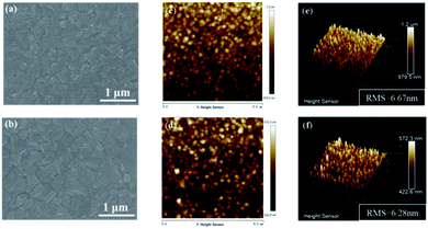
The high quality SnO2 ETL in PSCs should not only transport the photo-generated electrons effectively but also block the holes to reduce the carrier recombination. The surface of the SnO2 layer has a significant effect on the morphology topography of the perovskite film, which is associated with the performance of PSCs.33,34 In this work, SnO2 has been prepared by hydrothermal synthesis and modified with ytterbium chloride solution (refer to the Experimental part for detail). By a one-step solution spin-coating method, the perovskite films have been coated onto SnO2 and Yb-doped SnO2 substrates in ambient conditions. According to the SEM images shown in Fig. 1a and b, there are evident differences between the perovskite films on SnO2 and Yb-doped SnO2 ETL. Cracks can be formed among the perovskite crystalline coated onto the SnO2 ETL, which would increase the risk of physical contact between ETL and HTL. It is gratifying that tightly arranged crystalline grains have been obtained in the perovskite film coated onto Yb-doped SnO2. Compact and dense perovskite film is beneficial to efficiently convert light to electricity and decrease the nonradiative recombination, especially in the cracks of perovskite film. As shown in Fig. 1c–f, AFM images have also been collected to further observe the surface morphology of perovskite films. The surface roughness (RMS) value of perovskite films prepared on Yb-doped SnO2 is 6.28 nm, which is smaller than that of perovskite films fabricated on SnO2. It means that smoother perovskite film can be obtained onto the Yb-doped ETL, which is beneficial for constructing high-efficiency PSCs.
 |
| | Fig. 1 SEM images of perovskite films spin-coated on (a) SnO2 substrates and (b) Yb-doped SnO2 substrates, AFM images of perovskite films spin-coated on (c) SnO2 substrates and (d) Yb-doped SnO2 substrates, the surface roughness (RMS) of perovskite films spin-coated on (e) SnO2 substrates and (f) Yb-doped SnO2 substrates. | |
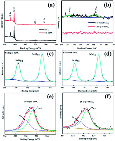
According to the XRD results of perovskite films on these two different SnO2 substrates (Fig. 2a), there are characteristic diffraction peaks located at 14.1°, 23.4°, 24.5°, 28.5°, 31.6°, 40.4°, and 43.1°, corresponding to the (110), (211), (202), (220), (310), (224), and (314) lattice planes of tetragonal phase CH3NH3PbI3, respectively.35,36 Almost no difference can be found in the crystalline structure of perovskite, even on different SnO2 substrates. As shown in Fig. 2b, the optical absorption of MAPbI3 film on Yb-SnO2 ETL is slightly enhanced in the range of 500–750 nm wavelength compared with that of the MAPbI3 film on SnO2 ETL. Both the absorption edges are located at around 800 nm, which matches well with the band gap of tetragonal CH3NH3PbI3 (1.51 eV). To evaluate the doping effect of Yb, the surface chemical and electronic states of SnO2 have been surveyed through XPS test, as shown in Fig. 3, which can act seriously on the carrier transfer and recombination processes in PSCs. As shown in Fig. 3a, Sn 3d and O 1s core electrons can be detected from the full XPS spectra of Yb-doped and undoped SnO2 films. In order to reveal the successful introduction of Yb3+ ions, the XPS test results of SnO2 films with and without Yb3+ ions are presented in Fig. 3b. The existence of a Yb 4d peak with weak intensity at 190.9 eV for the Yb-doped SnO2 film indicates that a trace amount of Yb3+ ions is successfully introduced into the SnO2 film.37 XPS test can also be used as an effective technique to figure out these oxygen-induced defects in SnO2. In Sn 3d XPS spectra of both samples (Fig. 3c and d), the Sn 3d3/2 peak at 496.0 and Sn 3d5/2 peak at 486.6 eV are identified in agreement with tetravalent tin. The O 1s XPS spectra of undoped SnO2 and Yb-doped SnO2 are shown in Fig. 3e and f, which can be attributed to two O chemical states at 529.2 eV and 530.7 eV. The O 1s peak with a binding energy of 529.2 eV corresponds to the O–Sn–O bond (denoted as OSn–O), while the peak at 530.7 eV can be attributed to the oxygen vacancy (denoted as OV). Based on the peak area ratios of OSn–O and OV, the relative amount of each O state in the whole O 1s (OSn–O + OV) can be estimated (Table 1), among which the oxygen vacancy reflecting the oxygen-induced defect is closely related to the carrier transport and recombination. It turns out that the OV decreased from 30.47% for the pure SnO2 to 25.51% for Yb-doped SnO2. The oxygen-induced defects situated at the interface of SnO2 and perovskite may lead to the enhanced transport of the photo-generated carriers.38,39
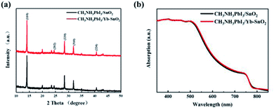 |
| | Fig. 2 (a) XRD patterns of perovskite films on pristine SnO2 and Yb-doped SnO2 film. (b) UV-Vis spectra of perovskite films on SnO2 and Yb-SnO2 ETLs, respectively. | |
 |
| | Fig. 3 Full XPS spectra of (a) the undoped SnO2 film and Yb-doped SnO2 film, (b) the Yb 4d of the SnO2 film and Yb-doped SnO2 film, (c) the Sn 3d of undoped SnO2, (d) the Sn 3d of Yb-doped SnO2, (e) the O 1s of undoped SnO2, and (f) the O 1s of Yb-doped SnO2. | |
Table 1 Peak position, area, and area ratio of OSn–O, OV, OO–H, for the undoped SnO2 and Yb-doped SnO2
| O 1s |
Undoped SnO2 |
Yb-doped SnO2 |
| OSn–O |
Position (eV) |
529.14 |
529.37 |
| Area |
3368.06 |
1746.12 |
| OV |
Position (eV) |
530.16 |
530.67 |
| Area |
1475.89 |
598.07 |
| OSn–O |
Area ratio (%) |
69.53 |
74.49 |
| OV |
Area ratio (%) |
30.47 |
25.51 |
Photovoltaic performance
Planar devices with FTO/Yb-doped SnO2 ETL/CH3NH3PbI3/spiro-OMeTAD/Au structure have been successfully constructed in air. To evaluate the photovoltaic parameters (AM 1.5 G illumination, 1 sun), the forward and reverse J–V curves of the control and Yb-doped devices have been collected and shown in Fig. 4a, and the photovoltaic parameters, including PCE, Voc, Jsc, and FF are summarized in Table 2. The champion device based on control SnO2 presents a PCE of 15.69% with a Voc of 1.03 V, a Jsc of 20.55 mA cm−2, and a FF of 74.13% under the reverse scan, while the champion device with Yb achieves a more superior PCE of 17.31% with a Jsc of 21.85 mA cm−2, a Voc of 1.06 V, and a FF of 74.40%. It is clear that the Voc and PCE have been improved significantly with the addition of Yb. More notably, the hysteresis index (HI = (PCEreverse − PCEforward)/PCEreverse) of Yb-SnO2-based device is reduced to 3.52%, compared to 9.88% of the control SnO2 device. It has been found that interface defects and charge accumulation are important factors causing hysteresis.40 Thus, the lower HI of the Yb-SnO2 device reflects that Yb dopants can effectively promote charge transport and can effectively reduce interface defects, which is confirmed by PL and time-resolved photoluminescence (TRPL). The hysteresis of J–V curves for the Yb-doped device is smaller than that of the SnO2 device. It has been found that the hysteresis effect is associated with the interfacial defects and quality of perovskite films.41,42 As demonstrated in the SEM and AFM images, the smoother perovskite film and larger grains can be obtained easily onto the Yb-doped SnO2 ETL. Additionally, the oxygen-induced defects located at the ETL/perovskite interface have been decreased successfully by Yb doping, which would accelerate the extraction of photo-induced electrons and suppress the recombination of carriers at the interface.43 Moreover, the hysteresis effect of J–V curves under forward and reverse scanning for the optimized device has also been significantly alleviated compared with the control device. In addition to the interface defects, the interfacial electric field, especially built-in potential in the device, is also closely related to the carrier transport and recombination, which can be speculated from the surface potential changes of SnO2 films tested by scanning Kelvin probe microscopy (SKPM).44 According to the test results in Table S1,† the surface work function values of SnO2 and Yb-SnO2 have been estimated. After Yb doping, the work function of SnO2 drops slightly from 4.28 eV to 4.17 eV. As described in the literature, the decrease in the work function of ETL always corresponds to the enhancement of built-in potential in the device.45 This enhanced built-in potential can not only speed up electron extraction but also make the detrapping of electrons, consequently suppressing the interface recombination caused by the defects.46 This enhanced built-in potential is reflected in the open-circuit voltage improvement of Yb-doped devices according to the above J–V results. The hysteresis in the J–V measurement leads to the instability of devices, which seriously hinders the application of PSCs. As reported, ion migration, defects at the interface, and accumulated unbalanced charge carriers are the three main sources of hysteresis in PSCs.47,48 In the optimized devices, the defect passivation of SnO2/perovskite interface and removal of residual hydroxyl will undoubtedly accelerate the interface electron extraction, leading to the reduction of hysteresis effect. As shown in Fig. 4c, IPCE spectra of the control and optimized devices show the same light-response range from 300 nm to 850 nm. The IPCE value of the optimized device is about 75–85%, which is higher than the 60–70% of the control device. According to the IPCE spectra, the integral current of 19.30 mA cm−2 for the original device and 20.20 mA cm−2 for the optimized device can be calculated, which is consistent with the J–V testing results. To evaluate the operating stability of the devices, 200 s maximum power point tests have been carried out (Fig. 4b), indicating both devices show a stable power output. However, the saturation time for the Yb-doped device is shorter than that of the SnO2 device. The faster carrier separation and extraction profited by the enhanced built-in potential in the optimized device leads to the quicker climbing to the maximum power point. In addition, the PCEs of 30 control or optimized devices have been independently collected to plot the histogram. As shown in Fig. 4d, the J–V curves of the control and Yb-doped devices have been collected and shown in Fig. 4d and S1–S3,† and the average photovoltaic parameters, including PCE, Voc, Jsc, and FF are summarized in Table S2.† The average parameters of devices based on control SnO2 present a PCE of 12.63%, with a Voc of 0.98 V, a Jsc of 19.12 mA cm−2, and a FF of 67.16%, while average parameters of Yb-doped devices present a more superior PCE of 14.92% with a Jsc of 20.24 mA cm−2, a Voc of 1.01 V, and a FF of 72.60%. The PCEs of optimized devices are distributed in the range of 14–16%, which is better than the control devices at 11–14%.
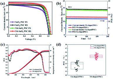 |
| | Fig. 4 (a) J–V curves with forward and reverse scan under the 0.2 V s−1 scan rate, (b) steady-state photocurrent density and power outputs, (c) IPCE spectra, (d) PCE histograms of PSCs. | |
Table 2 Champion performance of SnO2 device and Yb-doped based device
| Type |
Jsc (mA cm−2) |
Voc (V) |
FF (%) |
PCE (%) |
| SnO2 device reverse |
20.55 |
1.03 |
74.13 |
15.69 |
| SnO2 device forward |
20.51 |
1.02 |
67.88 |
14.14 |
| Yb-doped SnO2 device reverse |
21.85 |
1.06 |
74.40 |
17.31 |
| Yb-doped SnO device forward |
21.81 |
1.05 |
73.23 |
16.70 |
Carrier transport and recombination
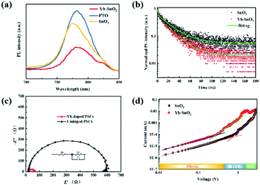
According to PL intensity of perovskite at different substrates (FTO, SnO2/FTO, and Yb-doped SnO2/FTO, Fig. 5a), the electronic extraction ability of ETL in PSCs can be evaluated. The weaker intensity in PL means the stronger electron extraction ability of ETLs.49 In general, defects or traps in the crystal structure cause quenching of PL,50 which lead to a reduced PL intensity and a shortened PL lifetime of photogenerated carriers in the absorber layer because it is an additional nonradiative de-excitation path for carriers. Here, the enhancement of PL intensity and growth of fluorescence lifetime implies that Yb3+ processed interface between ETL and perovskite film can effectively reduce the densities of traps, thereby decreasing the nonradiative recombination of carriers. Compared with the PL intensity of perovskite film on the FTO substrate, the perovskite film onto SnO2 ETL reveals an obvious quenching effect in the PL spectra. It is worth noting that Yb-doped SnO2, as an ETL, has a stronger quenching effect compared with the original SnO2, which means that photoinduced electron extraction of Yb-doped SnO2 ETL is more efficient. Furthermore, the TRPL results in Fig. 5b also further confirm that this Yb-doped SnO2 ETL has better electron extraction capability. It is generally believed that faster electron extraction in the optimized device can reduce the risk of electron accumulation and recombination at the ETL/perovskite interface. In order to study the recombination of carriers in photovoltaic devices, dark EIS has been measured within the frequency range of 0.1 Hz to 100 kHz. According to the Nyquist plots (Fig. 5c), only one semicircle is presented identical to that reported in the literature,51 of which the equivalent circuit has been inserted in Fig. 5c. The recombination resistances in control and optimized devices can be estimated by the size of the semicircle, and the larger one means the bigger the recombination resistance.52,53 Obviously, the optimized device shows a bigger recombination resistance. As demonstrated above, defect passivation and enhanced built-in potential can suppress carrier recombination at the SnO2/perovskite interface. To further understand the trap density of SnO2 ETL, space-charge-limited current (SCLC) measurements of FTO/SnO2 or Yb-doped SnO2/perovskite/PCBM/Au devices are carried out (Fig. 5d). In the range of low bias voltages, the linear relationship (black and orange line) of current and voltage represents the ohmic response of electron-only devices. When the bias voltage exceeds the kink point (trap-filled limit, TFL), the current rapidly increases nonlinearly (green and pink line), suggesting that the trap state is completely filled by the injected carriers. At high fields, the current showed a quadratic voltage dependence in the Child's regime (yellow line). The trap density (Nt) can be calculated by the trap-filled limit voltage (VTFL) using eqn (1).| |
 | (1) |
where e is the elementary charge of the electron, Nt is the trap-state density, L is the thickness of perovskite film, ε is the relative dielectric constant of MAPbI3 (ε = 32), and ε0 is the vacuum permittivity. The VTFL of the perovskite films is reduced from 0.71 V of pure SnO2 to 0.27 V with Yb-doped SnO2, corresponding to the Nt of 1.57 × 1016 cm−3 and 5.98 × 1015 cm−3, respectively. The lower trap density is attributed to the smoother interface, which helps to increase the contact between perovskite and the Yb-SnO2 ETL layer. The above characterization results all indicate that SnO2 has been effectively passivated by Y doping, resulting in less recombination and faster transfer of the photon-generating carriers in the device. This passivation of defects in SnO2 can remove the obstacles in the process of electron transport and the accumulation of interface charges.
 |
| | Fig. 5 (a) PL and (b) TRPL spectra of perovskite films onto FTO/SnO2 FTO/Yb-doped SnO2, (c) Nyquist plots of pristine PSC and Yb-PSC acquired from the dark EIS measurement under a bias of −0.9 V, (d) SCLC curves for the device of FTO/pristine SnO2 or Yb-doped SnO2/perovskite/PCBM/Au. | |
We further used steady-state PL and TRPL to analyze the charge generation and recombination kinetics of perovskite films deposited on different ETLs substrates (Fig. 5b). The PL intensity of FTO/Yb-SnO2/perovskite film is obviously lower than that of the FTO/SnO2/perovskite, indicating more effective electron extraction and transfer. This may be due to the better interface between the perovskite layer and the SnO2 layer, meanwhile, the TRPL curves are fitted by a biexponential decay function, given as eqn (2):
| |
 | (2) |
where
Ai is the decay amplitude and
τi is the PL decay time. The average PL decay lifetime (
τave) is evaluated by the
Ai and
τi values using
eqn (3). The corresponding detailed parameters are summarized in
Table 3.
| |
 | (3) |
Table 3 Values for TRPL characteristics of perovskite films deposited on Yb-SnO2 and SnO2
| ETL |
τave (ns) |
τ1 (ns) |
A1 |
τ2 (ns) |
A2 |
| SnO2 |
22.38 |
1.15 |
0.47 |
23.28 |
0.55 |
| Yb-SnO2 |
19.08 |
2.78 |
0.34 |
20.53 |
0.52 |
The result shows that the τave of SnO2-based perovskite film is 22.38 ns, while that of Yb-doped SnO2-based perovskite film is merely 3.3 ns. In addition, the ratio of τ1 is far outweighing than that of τ2. It suggests that a faster electron transfer occurs at the interface of Yb-doped SnO2/perovskite film, which can effectively reduce the accumulation of charge at the interface, so it is expected to extremely reduce the device hysteresis.
Stability
The instability of PSCs is one of the biggest challenges in practical applications due to the fragile perovskite material, which breaks down easily in case of moisture, oxygen, heating, and illumination. Through appropriate encapsulation, the perovskite device can avoid getting in touch with moisture and oxygen.54 However, the instability of perovskite material under heating and illumination is difficult to solve only by encapsulation, which has become a bottleneck that impedes the practical application of PSC.55 Although 85 °C is the common testing temperature for photovoltaic panels,56 we measured PSCs at 100 °C to accelerate ageing within a short time. As shown in Fig. 6a and b, the heating and illumination stability of control and optimized devices were tested in the air without any encapsulation. According to the 100 °C-heating test results, the optimized devices can maintain 83% of the original PCE after 7 hour heating, of which photovoltaic parameters remain relatively stable. However, the PCE of the control device drops dramatically to less than 15% of the original value after 4 hour heating. The sharp decline of FF, Voc and Jsc all indicate the serious degradation of the devices. Similarly, the optimized devices under illumination also reveal stable output, showing more than 80% original PCE value even after 7 hour illumination (Fig. 6b). By contrast, the degradation of control devices under illumination is even more pronounced. As demonstrated above, the introduction of Yb3+ can reduce the oxygen vacancy concentration of SnO2/perovskite interface, which is the active site of perovskite decomposition, especially under illumination. As displayed in Fig. S4,† the PCE of the Yb-doped SnO2 device maintains 90.25% of the original PCE after 28 days, and by contrast, the SnO2 device only maintains 46.60%. Obviously, the Yb-doped SnO2 device shows better air long-term stability. Similarly, Yb3+ ions also play a positive role in reducing interface trap states and inhibiting the degradation of perovskite films. Finally, stable planar PSCs can be prepared in air efficiently through this simple interface modification.
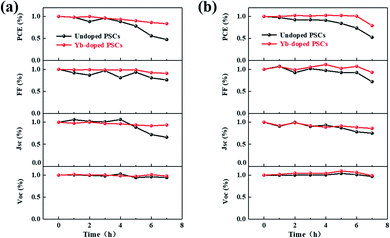 |
| | Fig. 6 (a) Thermostability (heating at 100 °C) and (b) illumination stability (AM 1.5 G illumination, 100 mW cm−2) tests of control and optimized devices. | |
Conclusion
In conclusion, we studied the Yb-doping effect on the morphology, electrical, and optical properties of SnO2 ETL and demonstrated the improvement of device efficiency and stability via this doping strategy. High-quality large-grain perovskite films have been successfully prepared on Yb-doped SnO2 ETL and the planar devices of FTO/Yb-doped SnO2/CH3NH3PbI3/spiro-OMeTAD/Au have been assembled in air. The interface defects in the optimized device have been suppressed effectually, accelerating the extraction of photo-induced electrons and inhibiting the nonradiative recombination in the device. Finally, the champion device with an ETL of Yb-doped SnO2 yields a PCE of 17.31%, which is much higher than the 15.69% PCE of the control device. Furthermore, the decrease of oxygen vacancy in the optimized device can lessen the risks of perovskite decomposition and promote device stability. It is noticed particularly that heating and illumination stabilities of optimized devices have also been improved markedly, which is of significant meaning in future applications, considering the all air-processed fabrication.
Conflicts of interest
There are no conflicts to declare.
Acknowledgements
This work is supported by the Natural Science Foundation of Heilongjiang Province of China (LH2021E054).
References
- L. Etgar, P. Gao, Z. Xue, Q. Peng, A. K. Chandiran, B. Liu, M. K. Nazeeruddin and M. Grätzel, J. Am. Chem. Soc., 2012, 134, 17396–17399 CrossRef CAS PubMed
 .
. - A. Polman, M. Knight, E. C. Garnett, B. Ehrler and W. C. Sinke, Science, 2016, 352, aad4424 CrossRef PubMed
 .
. - A. Kojima, K. Teshima, Y. Shirai and T. Miyasaka, J. Am. Chem. Soc., 2019, 131, 6050–6051 CrossRef PubMed
 .
. - S. Wang, Y. Jiang, E. J. Juarez-Perez, L. K. Ono and Y. B. Qi, Nat. Energy, 2016, 2, 16195 CrossRef
 .
. - Z. Xiao, Z. Song and Y. Yan, Adv. Mater., 2019, 31, 1803792 CrossRef CAS PubMed
 .
. - Q. Fan, G. V. Biesold-McGee, J. Ma, Q. Xu, S. Pan, J. Peng and Z. Lin, Angew. Chem., Int. Ed. Engl., 2020, 59, 1030–1046 CrossRef CAS PubMed
 .
. - B. W. Park and S. I. Seok, Adv. Mater., 2019, 31, 1805337 CrossRef PubMed
 .
. - R. Wang, M. Mujahid, Y. Duan, Z.-K. Wang, J. Xue and Y. Yang, Adv. Funct. Mater., 2019, 29, 1808843 CrossRef CAS
 .
. - Y. Zhou and Y. Zhao, Energy Environ. Sci., 2019, 12, 1495–1511 RSC
 .
. - T. H. Han, S. Tan, J. Xue, L. Meng, J. W. Lee and Y. Yang, Adv. Mater., 2019, 31, 1803515 CrossRef CAS PubMed
 .
. - A. K. Jena, A. Kulkarni and T. Miyasaka, Chem. Rev., 2019, 119, 3036–3103 CrossRef CAS PubMed
 .
. - H. D. Pham, X. Q. Li, W. H. Li, S. Manzhos, A. K. K. Kyaw and P. Sonar, Energy Environ. Sci., 2019, 12, 1177–1209 RSC
 .
. - D. Luo, R. Su, W. Zhang, Q. Gong and R. Zhu, Nat. Rev. Mater., 2020, 5, 44–60 CrossRef CAS
 .
. - J. Chen and N. G. Park, Adv. Mater., 2019, 31, 1803019 CrossRef CAS PubMed
 .
. - L. K. Ono, S. Liu and Y. Qi, Angew. Chem., Int. Ed., 2020, 59, 6676–6698 CrossRef CAS PubMed
 .
. - S. Singh, L. Laxmi and D. Kabra, J. Phys. D: Appl. Phys., 2020, 53, 503003 CrossRef
 .
. - E. Aydin, M. De Bastiani and S. De Wolf, Adv. Mater., 2019, 31, 1900428 CrossRef PubMed
 .
. - X. Hu, H. Wang and M. Wang, et al., Sol. Energy, 2020, 206, 816–825 CrossRef CAS
 .
. - M. Wang, W. Li and H. Wang, et al., Adv. Electron. Mater., 2020, 2000604 CrossRef CAS
 .
. - X. Hu, H. Wang and Y. Ying, et al., J. Power Sources, 2020, 480, 229073 CrossRef CAS
 .
. - T. Zhou, Y. Zhang and M. Wang, et al., J. Power Sources, 2019, 429, 120–126 CrossRef CAS
 .
. - X. D. Ren, D. Yang, Z. Yang, J. S. Feng, X. J. Zhu, J. Z. Niu, Y. C. Liu, W. G. Zhao and S. F. Liu, ACS Appl. Mater. Interfaces, 2017, 9, 2421–2429 CrossRef CAS PubMed
 .
. - Y. Lv, H. Tong, W. Cai, Z. Zhang, H. Chen and X. Zhou, J. Alloys Compd., 2021, 851, 156785 CrossRef CAS
 .
. - S. K. Pathak, A. Abate, P. Ruckdeschel, B. Roose, K. C. Godel, Y. Vaynzof, A. Santhala, S. I. Watanabe, D. J. Hollman, N. Noel, A. Sepe, U. Wiesner, R. Friend, H. J. Snaith and U. Steiner, Adv. Mater., 2014, 24, 6046–6055 CAS
 .
. - P. Qin, A. L. Domanski, A. K. Chandiran, R. Berger, H. J. Butt, M. I. Dar, T. Moehl, N. Tetreault, P. Gao, S. Ahmad, M. K. Nazeeruddin and M. Grätzel, Nanoscale, 2014, 6, 1508–1514 RSC
 .
. - X. X. Gao, Q. Q. Ge, D. J. Xue, J. Ding, J. Y. Ma, Y. X. Chen, B. Zhang, Y. Feng, L. J. Wan and J. S. Hu, Nanoscale, 2016, 8, 16881–16885 RSC
 .
. - B. Roose, K. C. Gödel, S. Pathak, A. Sadhanala, J. P. C. Baena, B. D. Wilts, H. J. Snaith, U. Wiesner, M. Grätzel, U. Steiner and A. Abate, Adv. Energy Mater., 2016, 6, 1501868 CrossRef
 .
. - Z. Ren, J. Wu, N. Wang and X. Li, J. Mater. Chem. A, 2018, 6, 15348–15358 RSC
 .
. - Y. H. Cheng, F. So and S. W. Tsang, Mater. Horiz., 2019, 6, 1611–1624 RSC
 .
. - W. Y. Zhang, Y. C. Li, X. Liu, D. Y. Tang, X. Li and X. Yuan, Chem. Eng. J., 2020, 379, 9 Search PubMed
 .
. - Z. Ren, M. Zhu, X. Li and C. Dong, J. Power Sources, 2017, 363, 317–326 CrossRef CAS
 .
. - Z. Ren, N. Wang, M. Zhu, X. Li and J. Qi, Electrochim. Acta, 2018, 282, 653–661 CrossRef CAS
 .
. - G. Yang, C. L. Wang, H. W. Lei, X. L. Zheng, P. L. Qin, L. B. Xiong, X. Z. Zhao, Y. F. Yan and G. J. Fang, J. Mater. Chem. A, 2017, 5, 1658–1666 RSC
 .
. - M. Yu, Y. R. Guo, S. Yuan, J. S. Zhao, Y. J. Qin and X. C. Ai, RSC Adv., 2020, 10, 12347–12353 RSC
 .
. - T. Baikie, Y. Fang, J. M. Kadro, M. Schreyer, F. Wei, S. G. Mhaisalkar, M. Graetzel and T. J. White, J. Mater. Chem. A, 2013, 1, 5628–5641 RSC
 .
. - A. M. A. Leguy, Y. Hu, M. Campoy-Quiles, M. I. Alonso, O. J. Weber, P. Azarhoosh, M. van Schilfgaarde, M. T. Weller, T. Bein, J. Nelson, P. Docampo and P. R. F. Barnes, Chem. Mater., 2015, 27, 3397–3407 CrossRef CAS
 .
. - S. H. Liang, D. F. Zhang, X. T. Yao, R. T. Han, Q. D. Zhang, C. Y. Jin, X. P. Pu and Y. L. Geng, Sep. Purif. Technol., 2020, 238, 116399 CrossRef
 .
. - Q. Sun, P. Fassl, D. Becker-Koch, A. Bausch, B. Rivkin, S. Bai, P. E. Hopkinson, H. J. Snaith and Y. Vaynzof, Adv. Energy Mater., 2017, 7, 1700977 CrossRef
 .
. - N. Aristidou, C. Eames, I. Sanchez-Molina, X. N. Bu, J. Kosco, M. S. Islam and S. A. Haque, Nat. Commun., 2017, 8, 15218 CrossRef PubMed
 .
. - P. Liu, W. Wang, S. Liu, H. Yang and Z. Shao, Adv. Energy Mater., 2019, 9, 180301713 Search PubMed
 .
. - J. M. Azpiroz, E. Mosconi, J. Bisquert and F. De Angelis, Energy Environ. Sci., 2015, 8, 2118–2127 RSC
 .
. - X. J. She, C. Chen, G. Divitini, B. Zhao, Y. Li, J. Wang, J. F. Orri, L. Cui, W. Xu, J. Peng, S. Wang, A. Sadhanala and H. Sirringhaus, Nat. Electron., 2020, 3, 694–703 CrossRef CAS
 .
. - C. T. Lin, F. De Rossi, J. Kim, J. Baker, J. Ngiam, B. Xu, S. Pont, N. Aristidou, S. A. Haque, T. Watson, M. A. McLachlan and J. R. Durrant, J. Mater. Chem. A, 2019, 7, 3006–3011 RSC
 .
. - Z. Q. Ren, N. Wang, P. C. Wei, M. H. Cui, X. Li and C. C. Qin, Chem. Eng. J., 2020, 393, 9 CrossRef
 .
. - W. Zhang, Z. Ren and G. Yan, et al., Electrochim. Acta, 2018, 268, 539–545 CrossRef CAS
 .
. - G. Yang, C. Wang, H. Lei, X. Zheng, P. Qin, L. Xiong, X. Zhao, Y. Yan and G. Fang, J. Mater. Chem. A, 2017, 5, 1658–1666 RSC
 .
. - E. L. Unger, E. T. Hoke, C. D. Bailie, W. H. Nguyen, A. R. Bowring, T. Heumuller, M. G. Christoforo and M. D. McGehee, Energy Environ. Sci., 2014, 7, 3690–3698 RSC
 .
. - H. J. Snaith, A. Abate, J. M. Ball, G. E. Eperon, T. Leijtens, N. K. Noel, S. D. Stranks, J. T. W. Wang, K. Wojciechowski and W. Zhang, J. Phys. Chem. Lett., 2014, 5, 1511–1515 CrossRef CAS PubMed
 .
. - Q.-D. Dao, A. Fujii, R. Tsuji, Y. Takeoka and M. Ozaki, Org. Electron., 2017, 43, 156–161 CrossRef CAS
 .
. - W. Zhang and Y. Li, et al., Chem. Eng. J., 2019, 379, 122298 CrossRef
 .
. - G. Niu, W. Li, F. Meng, L. Wang, H. Dong and Y. Qiu, J. Mater. Chem. A, 2014, 2, 705–710 RSC
 .
. - J. A. Christians, R. C. M. Fung and P. V. Kamat, J. Am. Chem. Soc., 2014, 136, 758–764 CrossRef CAS PubMed
 .
. - H. M. Yi, D. Wang, M. A. Mahmud, F. Haque, M. B. Upama, C. Xu, L. P. Duan and A. Uddin, ACS Appl. Energy Mater., 2018, 1, 6027–6039 CrossRef
 .
. - Y. Han, S. Meyer, Y. Dkhissi, K. Weber, J. M. Pringle, U. Bach, L. Spiccia and Y. B. Cheng, J. Mater. Chem. A, 2015, 3, 8139–8147 RSC
 .
. - X. D. Li, S. Fu, S.
Y. Liu, Y. L. Wu, W. X. Zhang, W. J. Song and J. F. Fang, Nano Energy, 2019, 64, 103962 CrossRef CAS
 .
. - C. C. Boyd, R. Cheacharoen and T. Leijtens, Chem. Rev., 2019, 119, 3418–3451 CrossRef CAS PubMed
 .
.
Footnotes |
| † Electronic supplementary information (ESI) available: Table S1 work function of SnO2 and Yb-doped SnO2 film. See https://doi.org/10.1039/d2ra01297a |
| ‡ These authors contributed equally to this work. |
|
| This journal is © The Royal Society of Chemistry 2022 |
Click here to see how this site uses Cookies. View our privacy policy here.  Open Access Article
 *a
*a
![[thin space (1/6-em)]](https://www.rsc.org/images/entities/char_2009.gif) :
:![[thin space (1/6-em)]](https://www.rsc.org/images/entities/char_2009.gif) 1) was then spin-coated at 500 rpm for 3 s and then at 3000 rpm for 60 s. 300 μL of ethyl acetate (anti-solvent) was dropped onto the spinning substrates at the first 16 s. After 25 min of annealing at 100 °C, shiny and dark brown perovskite films can be obtained. To prepare the HTL solution, 80 mg spiro-OMeTAD, 28.8 μL 4-tert-butylpyridine, and 17.4 μL Li–TFSi solution (520 mg in acetonitrile) were dissolved in 1 mL chlorobenzene, and then 50 μL HTL solution was spin-coated onto the perovskite layer at 3000 rpm for 20 s. Finally, 80 nm Au electrode was deposited via vacuum thermal evaporation. In this work, the planar devices with the structure of FTO/Yb-doped SnO2/CH3NH3PbI3/spiro-OMeTAD/Au were fabricated, measured, and stored totally in the air without any specific protection.
1) was then spin-coated at 500 rpm for 3 s and then at 3000 rpm for 60 s. 300 μL of ethyl acetate (anti-solvent) was dropped onto the spinning substrates at the first 16 s. After 25 min of annealing at 100 °C, shiny and dark brown perovskite films can be obtained. To prepare the HTL solution, 80 mg spiro-OMeTAD, 28.8 μL 4-tert-butylpyridine, and 17.4 μL Li–TFSi solution (520 mg in acetonitrile) were dissolved in 1 mL chlorobenzene, and then 50 μL HTL solution was spin-coated onto the perovskite layer at 3000 rpm for 20 s. Finally, 80 nm Au electrode was deposited via vacuum thermal evaporation. In this work, the planar devices with the structure of FTO/Yb-doped SnO2/CH3NH3PbI3/spiro-OMeTAD/Au were fabricated, measured, and stored totally in the air without any specific protection.


.
.
.
.
.
.
.
.
.
.
.
.
.
.
.
.
.
.
.
.
.
.
.
.
.
.
.
.
.
.
.
.
.
.
.
.
.
.
.
.
.
.
.
.
.
.
.
.
.
.
.
.
.
.
.
.

