
 Open Access Article
 This Open Access Article is licensed under a Creative Commons Attribution-Non Commercial 3.0 Unported Licence
Theoretical prediction of Janus PdXO (X = S, Se, Te) monolayers: structural, electronic, and transport properties
Tuan V. Vu ab,
Huynh V. Phucc,
Sohail Ahmadd,
Bui D. Hoie,
Nguyen V. Hieu*f,
Samah Al-Qaisig,
A. I. Kartamyshevab and
Nguyen N. Hieu*hi
ab,
Huynh V. Phucc,
Sohail Ahmadd,
Bui D. Hoie,
Nguyen V. Hieu*f,
Samah Al-Qaisig,
A. I. Kartamyshevab and
Nguyen N. Hieu*hi
aDivision of Computational Physics, Institute for Computational Science, Ton Duc Thang University, Ho Chi Minh City, Viet Nam. E-mail: vuvantuan@tdtu.edu.vn
bFaculty of Electrical & Electronics Engineering, Ton Duc Thang University, Ho Chi Minh City, Viet Nam
cDivision of Theoretical Physics, Dong Thap University, Cao Lanh, 870000, Viet Nam
dDepartment of Physics, College of Science, King Khalid University, P.O. Box 9004, Abha, Saudi Arabia. E-mail: sohail@kku.edu.sa
ePhysics Department, University of Education, Hue University, Hue, Viet Nam
fPhysics Department, The University of Danang–University of Science and Education, Da Nang, 550000, Viet Nam. E-mail: nvhieu@ued.udn.vn
gPalestinian Ministry of Education and Higher Education, Nablus, Palestine. E-mail: samah.qaisi@gmail.com
hInstitute of Research and Development, Duy Tan University, Da Nang, 550000, Viet Nam. E-mail: hieunn@duytan.edu.vn
iFaculty of Natural Sciences, Duy Tan University, Da Nang, 550000, Viet Nam
First published on 28th April 2022
Abstract
Due to the broken vertical symmetry, the Janus material possesses many extraordinary physico-chemical and mechanical properties that cannot be found in original symmetric materials. In this paper, we study in detail the structural, electronic, and transport properties of 1T Janus PdXO monolayers (X = S, Se, Te) by means of density functional theory. PdXO monolayers are observed to be stable based on the analysis of the vibrational characteristics and molecular dynamics simulations. All three PdXO structures exhibit semiconducting characteristics with indirect bandgap based on evaluations with hybrid functional Heyd–Scuseria–Ernzerhof (HSE06). The influences of the spin–orbit coupling (SOC) on the band diagram of PdXO are strong. Particularly, when the SOC is included, PdTeO is calculated to be metallic by the HSE06+SOC approach. With high electron mobility, Janus PdXO structures have good potential for applications in future nanodevices.
1 Introduction
The successful experimental synthesis of graphene1 is considered as one of the most important milestones for the field of materials science in general and two-dimensional (2D) layered nanostructures in particular in the 21st century. With many outstanding physical, mechanical, and physicochemical properties, graphene has been intensively studied for nearly the last 20 years. However, with zero bandgap and low carrier density at the Fermi level, it has been difficult to use graphene in nanoelectronic devices and also in superconducting technology. In parallel with figuring out the ways to overcome the graphene disadvantages, one has been continuously finding for other graphene-like structures. Consequently, a variety of new 2D nanostructures have been reported, such as silicene,2 germanene,3 stenene,4 post-transition metal monochalcogenides,5–8 and particularly transition metal dichalcogenides (TMDs).9,10 The 2D TMD monolayers possess many superior physical properties and electronic characteristics, which do not found in other layered materials.11–14In 2017, the asymmetric Janus TMD MoSSe has been experimentally reported,15,16 opening a new approach in the study of 2D layered structures. Immediately, many other 2D Janus structures were built and calculated using different theoretical and simulation methods.17–21 Due to the lacking of vertical symmetry, the symmetric structure of the Janus materials is reduced and is responsible for the appearance of many superior physical properties that cannot be observed in symmetric structures.22–24 The Janus In2SeTe, which can be built from InSe monolayer, possesses transport characteristics that are superior to InSe.22 Recently, the 1T pristine and Janus structures of the group VIII B dichalcogenides, including MX2 and MXY with M = Pt, Pd and X/Y are chalcogen elements, have received intensive attention because they have extraordinary physical characteristics with great potential applications in nanotechnology, such as thermoelectric devices or water splitting applications.25–27 However, although oxygen is a group VI element, studies have often focused on layered compounds based on chalcogen elements Se, Se, and Te. Particularly, recent studies have shown that oxygen-based layered materials are stable and possess many outstanding physical properties.20,23 The oxygenation of TMDs, such as WXO28 and MoSO29 or post-transition metal monochalcogenides such as In2XO23 and Ga2XO30 have been theoretically studied by density functional theory (DFT).
In this paper, we study the structural characteristics, electronic properties, and transport properties of 1T PdXO (X = S, Se, Te) monolayer by means of DFT calculations. The paper is organized as the following: Section 2 presents the computational methods of the study. The calculated results and discussion, including atomic structure and stability, electronic properties, and transport properties, are shown in Section 3. Finally, the conclusions of the investigation is shown in Section 4.
2 Computational method
The calculations of structural relaxation and electronic characteristics in this paper were based on the DFT approach as performed in the Quantum Espresso package.31 The interactions between electron and ion core were treated by the projector-augmented wave pseudo-potential method.32 The generalized gradient approximations of Perdew–Burke–Ernzerhof (PBE)33 were adopted to investigate the exchange-correlation function. To correct the electronic bands of the semiconductors, the Heyd–Scuseria–Ernzerhof functional (HSE06)34 was performed in the present work. We used the DFT-D2 method with van der Waals (vdW) correction35 to investigate the vdW interactions. A plane-wave cut-off of 70 Ry and (15 × 15 × 1) k-grid mesh was selected to sample the Brillouin zone of the studied materials. The atomic structures are fully relaxed as the residual forces were less than 10−3 eV Å−1. Further, the vertical vacuum spacing of 25 Å was used to eliminate interactions between periodic images of slabs. The phonon dispersions of the studied materials were evaluated via the density functional perturbation theory method.36 Ab-initio molecular dynamics (AIMD) simulations37 were also carried out at 300 K to evaluate thermal stability. The mobilities of carriers were calculated through the deformation potential approximation.383 Results and discussion
3.1 Atomic structure and stability
In the present study, we investigate the three 1T Janus PdXO (X = S, Se, Te) monolayers as shown in Fig. 1. They are the vertical asymmetric structures in which there is a significant difference in bond length between the Pd–X and Pd–O bonds. At the ground state, the lattice constant a of PdXO increases from 3.34 to 3.58 Å as the chalcogen (X) element moves from S to Te. This is due to the tendency to increase the Pd–X bond length in the compound with increasing atomic size of X. The calculated results for the structural parameters of the Janus PdXO monolayers are listed in Table 1.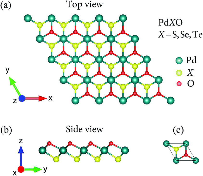 | ||
| Fig. 1 Atomic structures (a and b) and unitcell (c) of Janus monolayers PdXO (X = S, Se, Te). | ||
| a (Å) | dPd–X (Å) | dPd–O (Å) | φ∠Pd–O–Pd (deg) | φ∠Pd–X–Pd (deg) | Δh (Å) | Ec (eV) | |
|---|---|---|---|---|---|---|---|
| PdSO | 3.34 | 2.30 | 2.16 | 93.08 | 101.18 | 2.23 | −4.57 |
| PdSeO | 3.42 | 2.41 | 2.19 | 102.54 | 90.41 | 2.34 | −4.34 |
| PdTeO | 3.58 | 2.56 | 2.25 | 105.59 | 88.50 | 2.40 | −4.12 |
To examine the stabilities of the considered monolayers, we first evaluate the chemical bond strength through the calculations for cohesive energy. For Janus PdXO, the cohesive energy Ec is given by:
 | (1) |
Our calculated results show that the cohesive Ec of three Janus monolayers is all negative. This suggests that their structure is energetically favorable. The obtained value for the cohesive energies of PdXO is also tabled in Table 1. From Table 1, we can see that the chemical bonds in PdSO are stronger than those in other structures of PdXO.
The phonon dispersions of PdXO are shown Fig. 2, which allows us to consider their dynamical stabilities. The unit-cell of PdXO has three atoms, hence, their phonon dispersions have nine phonon branches, including three acoustic branches and six optical branches. As shown in Fig. 2, the acoustic modes are split from the optical branches by a quite large gap. The vibrational characteristics depend on the element size in the compound. Vibrations will be softer for elements with high atomic mass.39 Consequently, the vibrational frequencies are downshifted as increasing the atomic size of X element as shown in Fig. 2. More importantly, no negative frequencies (soft modes) are found in the phonon dispersions of all three investigated structures, suggesting that their structure is dynamically stable.
 | ||
| Fig. 2 Phonon dispersions of Janus PdXO monolayers. | ||
Based on the calculations of the elastic coefficients Cij, we use Born–Huang's criteria for the mechanical stability to test the mechanical stability of the studied structures. In the case of PdXO monolayers, there is two independent constants should be calculated, namely C11 and C12, because C22 = C11 and C66 is defined by C66 = (C11 − C12)/2. By fitting the values of strain-dependent elastic energy, we can get the elastic coefficients. This approach has been previously used to estimate the stiffness coefficients of similar systems.40–42 As listed in Table 2, we can see that Cij of PdXO depends strongly on the chalcogen element. Cij decreases with increasing atomic size of X element. The stiffness coefficients of all three PdX meet the Born–Huang's criteria for mechanical stability, namely C11 > 0 and C211 − C212 > 0,43 suggesting that the mechanical stability of all three studied monolayers are confirmed.
| C11 (Nm−1) | C12 (Nm−1) | C66 (Nm−1) | Y2D (Nm−1) | ν | |
|---|---|---|---|---|---|
| PdSO | 84.97 | 24.18 | 30.40 | 78.09 | 0.29 |
| PdSeO | 63.92 | 18.44 | 22.75 | 58.61 | 0.29 |
| PdTeO | 19.09 | 1.83 | 8.63 | 18.91 | 0.10 |
Young's modulus Y2D and Poisson's ratio ν for PdXO monolayers are given by43
 | (2) |
 | (3) |
It is found that, as listed in Table 2, Janus PdXO monolayers have small Young's modulus, from 18.91 to 58.09 N m−1. We can see that Y2D of PdXO is less than that of other 2D layered nanostructures, such as graphene (340 N m−1),44 MoS2 (130 N m−1),45 Janus MoSSe (113 N m−1),46 or Janus Ga2SO (155 N m−1).30 This suggests that Janus PdXO monolayers possess high flexibility and can be distorted with large amplitude.
Further, we also consider the thermal stability of PdXO monolayers, which is important when using these materials in real nanodevices. The thermal stability of PdXO is checked at room temperature (300 K) based on AIMD simulations. All structures are heated at room temperature within 6 ps by 6000 time-steps. In Fig. 3, we show the AIMD simulations for the time-dependence of the total energy at room temperature of all three Janus monolayers PdXO. It is found that the total energy fluctuates slightly during the heating period. Also, no significant distortion was detected and the structure of the Janus monolayers was still robust throughout the thermal investigation, implying that PdXO structures are thermally stable at room temperature.
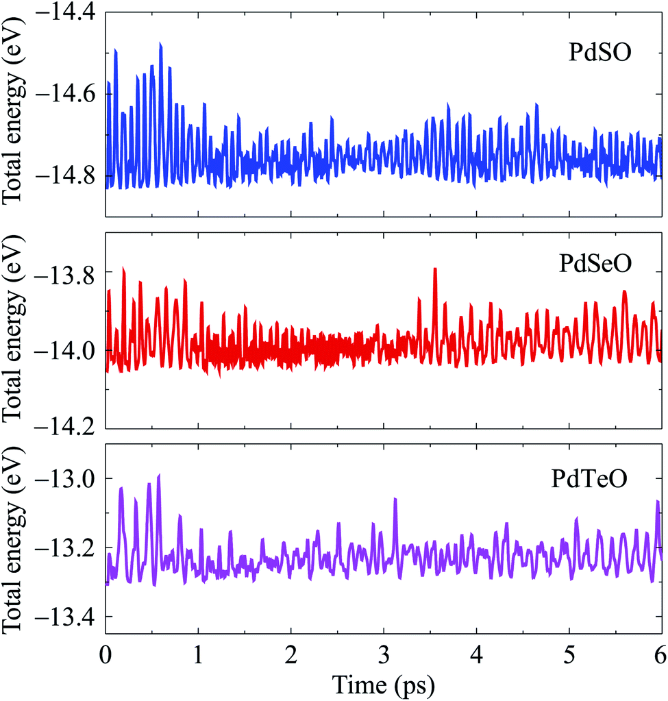 | ||
| Fig. 3 Time-dependence of the total energy of PdXO (X = S, Se, Te) by AIMD simulations. | ||
3.2 Electronic properties
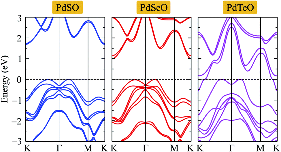
In this part, we study the electronic characteristics of PdXO by using the DFT calculations with different functionals. Fig. 4 shows the band diagrams of PdXO at the PBE and HSE06 levels. It is calculated that, at the PBE level, while both PdSO and PdSeO are semiconductors with indirect bandgaps, PdTeO possesses metallic characteristics. The PBE band gap of PdSO and PdSeO is 0.91 and 0.46 eV, respectively. Also, the calculated energy gap of Janus PdSeO is observed to be smaller than that of 1T-PdSe2 monolayer.47 However, the PBE functional in DFT calculations underestimates the energy gap issue. Therefore, the hybrid functional should be used to correct band diagram. In the present work, we use the HSE06 functional to correct the band diagram of PdXO as shown in Fig. 4. Our computed results reveals that the bandgap of PdSO and PdSeO is respectively 1.81 and 1.23 eV at the HES06 level. More interestingly, by using the HSE06 functional, PdTeO is a semiconductor with the narrow indirect bandgap of 0.36 eV. The calculated results for the bandgaps of PdXO are tabled in Table 3. From Fig. 4, we can observe that the band diagrams calculated by the HSE06 and PBE methods have a similar profile. The conduction band minimum (CBM) and valence band maximum (VBM) of the semiconductors are at the K-point and on the ΓK-path. | ||
| Fig. 4 Band diagrams (a) PdSe, (b) PdSeO, and (c) PdTeO at the PBE (left panel) and HSE06 (right panel) levels. | ||
| EPBEg | EHSE06g | EHSE06+SOCg | ΔΦ | ΦX | ΦO | |
|---|---|---|---|---|---|---|
| PdSO | 0.91 | 1.81 | 1.68 | 2.02 | 5.54 | 7.75 |
| PdSeO | 0.46 | 1.23 | 0.98 | 2.75 | 4.84 | 7.59 |
| PdTeO | Metal | 0.36 | Metal | 3.08 | 4.40 | 7.49 |
For the compound-based heavy element, such as Se or Te, the effect of SOC on the electronic properties is important. The band structures of PdXO calculated by the HSE06+SOC approach are illustrated in Fig. 5. We can observe that the band structures of PdX monolayers are substantially changed when the SOC is included. At the VBM and CBM, the spin degeneracy is removed owing to the SOC effect. The band splitting has been observed in the band structures of PdXO, especially in the cases of PdSe and PdTeO monolayers. The calculated band gap of PdSe and PdSeO by the HSE06+SOC method is found to be 1.68 and 0.923 eV, much smaller than their HSE06 band gap as listed in Table 3. Particularly, the Janus PdTeO monolayer becomes a metal when the SOC effect is taken into account.
 | ||
| Fig. 5 Band structures of PdXO calculated by the HSE06+SOC method. | ||
To get insights into the nature of the formation of the energy electronic bands as well as the atomic orbital contributions to the electronic bands, we evaluate the weighted bands of PdXO by using the HSE06 functional as shown in Fig. 6. It is demonstrated that the VBM of PdXO is highly donated by the O-p orbitals. Compared with the O-p contribution, the contribution of orbitals of Pd and X atoms to the valence band is smaller. Meanwhile, the Pd-d orbitals have a significant contribution to the CBM.
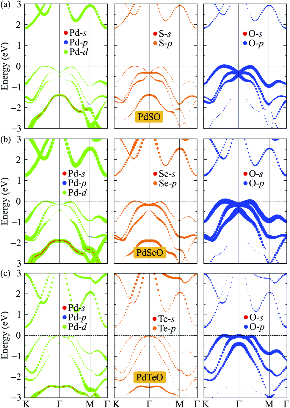 | ||
| Fig. 6 Weighted bands of (a) PdSe, (b) PdSeO, and (c) PdTeO at the HSE06 level. | ||
One of key parameters of electronic materials is work function Φ. Based on the work function, we can determine the conditions for the electrons to escape from the surface of the material. We can determine Φ via the Fermi level ΦF and vacuum level Φvac as the following:
| Φ = Φvac − ΦF | (4) |
Due to the vertical asymmetric structure, there is an internal electric field existing in the Janus monolayer. Fig. 7 presents the planar electrostatic potential with dipole correction of PdXO. The distinct vacuum level difference ΔΦ depends on the electronegativity of atomic layers on the two sides. It is found that ΔΦ increases with the increase of the difference in atomic size between X and O atoms. As listed in Table 3, ΔΦ increases from 2.02 to 3.08 eV as X moves from S to Te. In each structure, the work function on the X side (ΦX) is smaller than the work function on the O side (ΦO).
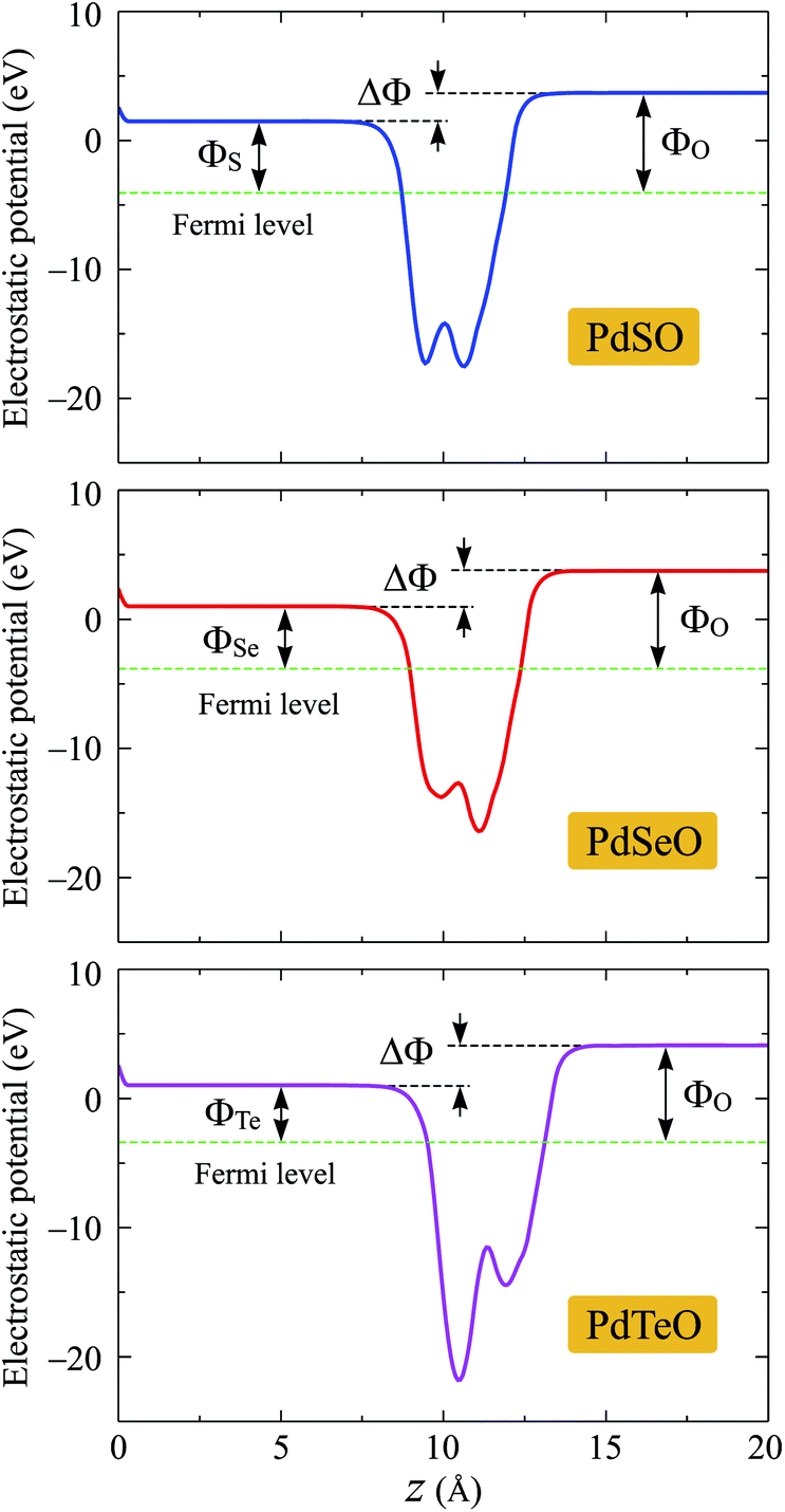 | ||
| Fig. 7 Planar electrostatic potential with dipole correction of PdXO (X = S, Se, Te). The difference in vacuum level between the X and O sides is denoted by ΔΦ. | ||
3.3 Transport properties
Transport characteristics of electronic properties are important, which determine the potential application of the materials in electronic devices. In this part, we focus on the carrier mobility, which can be considered through the deformation potential approximation.38 In the 2D nanomaterials, the carrier mobility is given by:22
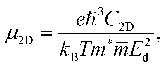 | (5) |
 All the calculations were carried out at T = 300 K (room temperature). We investigate the mobility of hole/electron along the two transport directions x/y.
The effective masses of carriers are quantity that depends on the band structure of near the c band-edges and we can obtain the effective masses by fitting linearly function to the CBM (electrons) and VBM (holes) via the formula as:
 | (6) |
As shown in eqn (7), it reveals that, the flatter the bands near the CBM/VBM (large curvature radius), the greater the effective masses of the carriers. The obtained results for the carrier effective mass m* are presented in Table 4. It is found that the effective mass is directionally isotropic for all studied structures. However, the electron effective mass  is much smaller than effective mass of holes
  , suggesting that the electrons respond to the external field faster and their mobility can be higher. The
  of PdSO is calculated to be 0.70m0, higher than that of both PdSe and PdTe as listed in Table 4.
|
|
Cx2D | Cy2D | Exd | Eyd | μx | μy | ||
|---|---|---|---|---|---|---|---|---|---|
| PdSO | Electron | 0.70 | 0.70 | 67.30 | 68.76 | −3.78 | −3.84 | 94.97 | 94.12 |
| Hole | 2.59 | 2.59 | 67.30 | 68.76 | −3.50 | −2.44 | 21.91 | 45.92 | |
| PdSeO | Electron | 0.57 | 0.57 | 58.80 | 59.10 | −3.08 | −3.11 | 215.90 | 212.29 |
| Hole | 2.43 | 2.43 | 58.80 | 59.10 | −3.58 | −2.54 | 25.08 | 50.09 | |
| PdTeO | Electron | 0.41 | 0.41 | 45.03 | 43.76 | −8.70 | −2.56 | 593.37 | 515.18 |
| Hole | 7.02 | 7.02 | 45.03 | 43.76 | −3.75 | −2.68 | 4.04 | 7.68 |

As shown in eqn (4), the mobility of carriers depends also on the elastic modulus C2D and deformation potential constant Ed. The elastic modulus C2D is written as
 | (7) |
The deformation potential constant Ed is calculated as:
 | (8) |
In Fig. 8, we present the obtained results for band-edge positions under small strain. It is found that there is no significant difference in the positions of band-edge between the x- and y-directions for PdSO and PdSeO. Meanwhile, there is a significant difference in the VBM position between the x- and y-directions in the case of PdTeO (about 0.01 eV at the uniaxial strain of ±1%). This leads to the difference between Exd and Eyd of PdTeO monolayer. The obtained results for C2D and Ed are tabled in Table 4.
 | ||
| Fig. 8 Strain-dependence of band-edge positions of PdXO structures along the two transport directions x and y. | ||
The obtained results for the mobility of carriers of PdXO monolayers μx and μy are tabled in Table 4. It is indicated that the mobility of the electron is much higher than that of the hole. This is because the electron mass is much smaller than the hole mass as above-mentioned. PdXO monolayers exhibit high electron mobility, up to 593.37 cm2 V−1 s−1 for PdTeO. The electron mobility of PdSO and PdSeO is highly directional isotropic, while the mobility of electron along the x direction of while PdTeO is slightly higher than that along the y direction. This is due to the significant difference in the Ed value between the two transport directions. Such slight anisotropy in carrier mobility has also been reported in the 2D isotropic structure WSiGeN4.48 It is noted that MoS2 monolayer with the mobility of the electrons of 200 cm2 V−1 s−1 was a perfect candidate for application in electronic nanodevices.49 Hence, with high electron mobility, PdXO monolayers have great potential for applications in next-generation electronic nanodevices.
4 Conclusion
In conclusion, the atomic structures, electronic properties, and transport characteristics of the PdXO have been theoretically studied based on the DFT simulations. The calculated results demonstrated that all three structures of PdXO were found to be dynamically and thermally stable and their elastic constants satisfied the criteria suggested by Born and Huang for mechanical stability. At the ground state, all three investigated structures are indirect semiconductors at the HSE06 level. As heavy element-based compounds, the effect of SOC on the electronic properties of PdXO, particularly PdTeO monolayer, is significant. With high electron mobility, up to 593.37 cm2 V−1 s−1 for PdTeO, Janus PdXO monolayers are suitable materials for applications in nanoelectronics.Conflicts of interest
There are no conflicts of interest to declare.Acknowledgements
Sohail Ahmad extends his appreciation to the Deanship of Scientific Research at King Khalid University for financial support through the research groups program under grant number (RGP2/139/43).References
- K. S. Novoselov, A. K. Geim, S. V. Morozov, D. Jiang, Y. Zhang, S. V. Dubonos, I. V. Grigorieva and A. A. Firsov, Science, 2004, 306, 666 CrossRef CAS PubMed.
- B. Lalmi, H. Oughaddou, H. Enriquez, A. Kara, S. Vizzini, B. Ealet and B. Aufray, Appl. Phys. Lett., 2010, 97, 223109 CrossRef.
- M. E. Dávila, L. Xian, S. Cahangirov, A. Rubio and G. Le Lay, New J. Phys., 2014, 16, 095002 CrossRef.
- F.-f. Zhu, W.-j. Chen, Y. Xu, C.-l. Gao, D.-d. Guan, C.-h. Liu, D. Qian, S.-C. Zhang and J.-f. Jia, Nat. Mater., 2015, 14, 1020–1025 CrossRef CAS PubMed.
- D. D. Vaughn, R. J. Patel, M. A. Hickner and R. E. Schaak, J. Am. Chem. Soc., 2010, 132, 15170 CrossRef CAS PubMed.
- P. Hu, L. Wang, M. Yoon, J. Zhang, W. Feng, X. Wang, Z. Wen, J. C. Idrobo, Y. Miyamoto, D. B. Geohegan and K. Xiao, Nano Lett., 2013, 13, 1649 CrossRef CAS PubMed.
- P. Hu, Z. Wen, L. Wang, P. Tan and K. Xiao, ACS Nano, 2012, 6, 5988 CrossRef CAS PubMed.
- S. Acharya, M. Dutta, S. Sarkar, D. Basak, S. Chakraborty and N. Pradhan, Chem. Mater., 2012, 24, 1779–1785 CrossRef CAS.
- D. Kong, H. Wang, J. J. Cha, M. Pasta, K. J. Koski, J. Yao and Y. Cui, Nano Lett., 2013, 13, 1341–1347 CrossRef CAS PubMed.
- G. Deokar, D. Vignaud, R. Arenal, P. Louette and J.-F. Colomer, Nanotechnology, 2016, 27, 075604 CrossRef CAS PubMed.
- C. V. Nguyen, N. N. Hieu, N. A. Poklonski, V. V. Ilyasov, L. Dinh, T. C. Phong, L. V. Tung and H. V. Phuc, Phys. Rev. B, 2017, 96, 125411 CrossRef.
- N. D. Hien, C. V. Nguyen, N. N. Hieu, S. S. Kubakaddi, C. A. Duque, M. E. Mora-Ramos, L. Dinh, T. N. Bich and H. V. Phuc, Phys. Rev. B, 2020, 101, 045424 CrossRef.
- T. V. Vu, N. V. Hieu, L. T. P. Thao, N. N. Hieu, H. V. Phuc, H. D. Bui, M. Idrees, B. Amin, L. M. Duc and C. V. Nguyen, Phys. Chem. Chem. Phys., 2019, 21, 22140–22148 RSC.
- C. V. Nguyen, N. N. Hieu, D. Muoi, C. A. Duque, E. Feddi, H. V. Nguyen, L. T. T. Phuong, B. D. Hoi and H. V. Phuc, J. Appl. Phys., 2018, 123, 034301 CrossRef.
- A.-Y. Lu, H. Zhu, J. Xiao, C.-P. Chuu, Y. Han, M.-H. Chiu, C.-C. Cheng, C.-W. Yang, K.-H. Wei, Y. Yang, Y. Wang, D. Sokaras, D. Nordlund, P. Yang, D. A. Muller, M.-Y. Chou, X. Zhang and L.-J. Li, Nat. Nanotechnol., 2017, 12, 744 CrossRef CAS PubMed.
- J. Zhang, S. Jia, I. Kholmanov, L. Dong, D. Er, W. Chen, H. Guo, Z. Jin, V. B. Shenoy, L. Shi and J. Lou, ACS Nano, 2017, 11, 8192–8198 CrossRef CAS PubMed.
- Dimple, N. Jena, A. Rawat, R. Ahammed, M. K. Mohanta and A. De Sarkar, J. Mater. Chem. A, 2018, 6, 24885–24898 RSC.
- N. N. Hieu, H. V. Phuc, A. I. Kartamyshev and T. V. Vu, Phys. Rev. B, 2022, 105, 075402 CrossRef CAS.
- T. V. Vu, N. V. Hieu, H. V. Phuc, N. N. Hieu, H. Bui, M. Idrees, B. Amin and C. V. Nguyen, Appl. Surf. Sci., 2020, 507, 145036 CrossRef CAS.
- T. V. Vu, V. T. T. Vi, H. V. Phuc, A. I. Kartamyshev and N. N. Hieu, Phys. Rev. B, 2021, 104, 115410 CrossRef CAS.
- H. T. T. Nguyen, V. V. Tuan, C. V. Nguyen, H. V. Phuc, H. D. Tong, S.-T. Nguyen and N. N. Hieu, Phys. Chem. Chem. Phys., 2020, 22, 11637–11643 RSC.
- W. Wan, S. Zhao, Y. Ge and Y. Liu, J. Phys.: Condens. Matter, 2019, 31, 435501 CrossRef CAS PubMed.
- T. V. Vu, C. V. Nguyen, H. V. Phuc, A. A. Lavrentyev, O. Y. Khyzhun, N. V. Hieu, M. M. Obeid, D. P. Rai, H. D. Tong and N. N. Hieu, Phys. Rev. B, 2021, 103, 085422 CrossRef CAS.
- H. T. T. Nguyen, M. M. Obeid, A. Bafekry, M. Idrees, T. V. Vu, H. V. Phuc, N. N. Hieu, L. T. Hoa, B. Amin and C. V. Nguyen, Phys. Rev. B, 2020, 102, 075414 CrossRef CAS.
- E. A. Moujaes and W. A. Diery, J. Phys.: Condens. Matter, 2019, 31, 455502 CrossRef CAS PubMed.
- S. Ahmad, Mater. Chem. Phys., 2017, 198, 162–166 CrossRef CAS.
- L. You, Y. Wang and K. Zhou, Phys. Status Solidi RRL, 2021, 2100344 Search PubMed.
- M. J. Varjovi, M. Yagmurcukardes, F. M. Peeters and E. Durgun, Phys. Rev. B, 2021, 103, 195438 CrossRef CAS.
- M. Yagmurcukardes and F. M. Peeters, Phys. Rev. B, 2020, 101, 155205 CrossRef CAS.
- M. Demirtas, B. Ozdemir, Y. Mogulkoc and E. Durgun, Phys. Rev. B, 2020, 101, 075423 CrossRef CAS.
- P. Giannozzi, S. Baroni, N. Bonini, M. Calandra, R. Car, C. Cavazzoni, D. Ceresoli, G. L. Chiarotti, M. Cococcioni, I. Dabo, A. D. Corso, S. de Gironcoli, S. Fabris, G. Fratesi, R. Gebauer, U. Gerstmann, C. Gougoussis, A. Kokalj, M. Lazzeri, L. Martin-Samos, N. Marzari, F. Mauri, R. Mazzarello, S. Paolini, A. Pasquarello, L. Paulatto, C. Sbraccia, S. Scandolo, G. Sclauzero, A. P. Seitsonen, A. Smogunov, P. Umari and R. M. Wentzcovitch, J. Phys.: Condens. Matter, 2009, 21, 395502 CrossRef PubMed.
- P. E. Blöchl, Phys. Rev. B, 1994, 50, 17953 CrossRef PubMed.
- J. P. Perdew, K. Burke and M. Ernzerhof, Phys. Rev. Lett., 1996, 77, 3865 CrossRef CAS PubMed.
- J. Heyd, G. E. Scuseria and M. Ernzerhof, J. Chem. Phys., 2003, 118, 8207 CrossRef CAS.
- S. Grimme, J. Comput. Chem., 2006, 27, 1787 CrossRef CAS PubMed.
- T. Sohier, M. Calandra and F. Mauri, Phys. Rev. B, 2017, 96, 075448 CrossRef.
- S. Nosé, J. Chem. Phys., 1984, 81, 511 CrossRef.
- J. Bardeen and W. Shockley, Phys. Rev., 1950, 80, 72 CrossRef CAS.
- A. Molina-Sánchez and L. Wirtz, Phys. Rev. B, 2011, 84, 155413 CrossRef.
- K.-A. N. Duerloo, M. T. Ong and E. J. Reed, J. Phys. Chem. Lett., 2012, 3, 2871–2876 CrossRef CAS.
- W.-Z. Xiao, G. Xiao and L.-L. Wang, J. Chem. Phys., 2016, 145, 174702 CrossRef PubMed.
- Y. Guo, S. Zhou, Y. Bai and J. Zhao, Appl. Phys. Lett., 2017, 110, 163102 CrossRef.
- R. C. Andrew, R. E. Mapasha, A. M. Ukpong and N. Chetty, Phys. Rev. B, 2012, 85, 125428 CrossRef.
- D. G. Papageorgiou, I. A. Kinloch and R. J. Young, Prog. Mater. Sci., 2017, 90, 75–127 CrossRef CAS.
- R. C. Cooper, C. Lee, C. A. Marianetti, X. Wei, J. Hone and J. W. Kysar, Phys. Rev. B, 2013, 87, 035423 CrossRef.
- S.-D. Guo and J. Dong, Semicond. Sci. Technol., 2018, 33, 085003 CrossRef.
- L.-Y. Feng, R. A. B. Villaos, Z.-Q. Huang, C.-H. Hsu and F.-C. Chuang, New J. Phys., 2020, 22, 053010 CrossRef CAS.
- S.-D. Guo, W.-Q. Mu, Y.-T. Zhu, R.-Y. Han and W.-C. Ren, J. Mater. Chem. C, 2021, 9, 2464–2473 RSC.
- B. Radisavljevic, A. Radenovic, J. Brivio, V. Giacometti and A. Kis, Nat. Nanotechnol., 2011, 6, 147–150 CrossRef CAS PubMed.
| This journal is © The Royal Society of Chemistry 2022 |