 Open Access Article
Investigating electrochemical deposition of gold on commercial off-the-shelf 3-D printing materials towards developing sensing applications†
Kristin Partanena,
Yu Peiab,
Phillip Hillena,
Malek Hassana,
Kevin McEleneya,
Gabriele Schattea,
Sarah Jane Payneab,
Richard Oleschuka and
Zhe She *a
*a
aDepartment of Chemistry, Queen's University, Chernoff Hall, Kingston, ON K7L 3N6, Canada. E-mail: zhe.she@queensu.ca
bDepartment of Civil Engineering, Queen's University, Ellis Hall, Kingston, ON K7L 3N6, Canada
First published on 22nd November 2022
Abstract
The COVID-19 pandemic highlighted the inaccessibility of quick and affordable clinical diagnostics. This led to increased interest in creating low-cost portable electrochemical (EC) devices for environmental monitoring and clinical diagnostics. One important perspective is to develop new fabrication methods for functional and low-cost electrode chips. Techniques, such as electron beam and photolithography, allow precise and high-resolution electrode fabrication; however, they are costly and can be time-consuming. More recently, fused deposition modeling three-dimensional (3-D) printing is being used as an alternative fabrication technique due to the low-cost of the printer and rapid prototyping capability. In this study, we explore enhancing the conductivity of 3-D printed working electrodes with EC gold deposition. Two commercial conductive filament brands were used and investigated to fabricate electrode chips. Furthermore, strategies to apply epoxy glue and conductive silver paint were investigated to control the electrode surface area and ensure good electrical connection. This device enables detection at drinking water concentration thresholds. The practical application of the fabricated electrodes is demonstrated by detecting Cu2+ using anodic stripping voltammetry.
Introduction
Quick and affordable diagnostic tests have recently gained interest due to their overwhelming need and inaccessibility at the onset of the COVID-19 pandemic.1 Portable electrochemical (EC) devices, such as glucose meters and lead drinking water analysers, have been widely used for household and industrial on-site monitoring.2,3 Electrode fabrication is one of the key components for building EC devices. Techniques, such as electron beam and photolithography, have been used to design features on chips with ultra-high resolution.4,5 The downside is that lithographic methods are costly, may require the use of a nanofabrication facility which limits accessibility, requires trained personnel, and are not as amenable to rapid prototyping.6,7 To reduce fabrication costs, Jeong et al. produced a low-cost microelectrode array (MEA) which used a laser-patterned indium tin oxide (ITO) substrate and SU-8 photoresist as insulation using photolithography.8 However, this method required the ITO to be deposited via sputtering by UID KOREA, limiting accessibility.8 Previously, our group fabricated an electrode chip using a combination of 3-dimensional (3-D) printing to create shadow masks with physical vapour deposition (PVD) to deposit gold onto glass slides.9 Even though 3-D printed shadow masks avoided photolithography, the PVD process still requires access to a clean room, and results in considerable gold waste. Improving previous methods would make electrode fabrication simpler, cheaper and more accessible.Screen printing technologies are favoured by the current chip fabrication industry, due to their ease of miniaturization, robustness, low-cost, reproducibility and their applicability for chemical and biological applications.10,11 For example, Alberti et al. and Kuralay et al. successfully used gold screen-printed electrodes (SPE) with a thiol self-assembled monolayer (SAM) to detect Fe3+ content in tap water and detect nucleic acid hybridization in biological samples.12,13 Even though SPEs are small and capable sensing elements, they still face the hurdles of limited 2-dimensional (2-D) ink printing designs. Therefore, it is useful to develop new low-cost methods that are customizable and tailored to biological and chemical sensing.
The incorporation of Fused Deposition Modelling (FDM) 3-D printing technology for chip fabrication is promising since it is cost-effective, fast enabling rapid prototyping and easy customization for 2-D and 3-D designs.14 Contreras-Naranjo et al. demonstrated a way to fabricate miniaturized 3-D printed hybrid-carbon based electrodes using an FDM 3-D printer for electroanalytical sensing purposes.14 However, the chip needed to first be pre-treated with dimethylformamide/phosphate-buffered saline to do electron transfer studies, since poor signal was obtained otherwise.14 Moreover, Martins et al. demonstrated an immunosensor for Hantavirus detection.15 They used a conductive 3-D carbon black polylactic acid (PLA) filament; however, it needed sodium hydroxide pre-treatment for surface activation. Overall, their electrodes showed proper EC potassium ferricyanide redox activity with good conductivity and an approximate current value of 25 μA with a surface area of about 102 mm2. We are looking at methods that can reduce electrode size using 3-D printing while maintaining good conductivity.
Numerous applications use gold electrodes as they are well-known in EC sensors because they provide high chemical stability, large surface area, exhibit good biocompatibility, and facilitate electron transfer between biomolecules and electrodes.16,17 Utilization of a gold electrode also allows for further modification of the EC sensor, such as forming SAMs for biosensing, to further expand potential applications of the sensor.18–20 Peng et al. fabricated a successful EC sensor based on gold nanoparticles modified with rhodamine B hydrazine for highly selective and sensitive detection of Cu2+.16 German et al. showed successful electrochemical deposition of gold nanoparticles on graphite rod for glucose biosensing.21 Therefore, it is advantageous to investigate depositing gold onto 3-D printed materials to help improve the conductivity, electron transfer, sensitivity, and stability of the electrode sensors.22–24
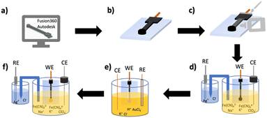
In this study, we investigated an alternative electrode fabrication method that combines 3-D printing with EC gold deposition to produce electrode chips shown in Fig. 1. Selecting suitable filaments, electrode designs, and controlling the gold deposition process to enhance the conductivity and gold surface coverage is challenging. This is because the current of the 3-D printing filaments lack sufficient conductivity for EC redox activity, however, gold deposition has potential to greatly increase the conductivity.25 This study demonstrates that fabricating a 3-D printed electrode chip using conductive carbon/PLA filament with electrochemical gold deposition, has the potential to be used in chemical and biological sensing platforms and applications.
Experimental
Reagents
Potassium nitrate (99%), agar (Fisher BioReagents™), potassium ferrocyanide trihydrate (98.5%, certified ACS), sulfuric acid (93–98%, trace metal grade) and potassium ferricyanide (99%, certified ACS) were purchased from Fisher Scientific (Ottawa, Ontario). Isopropyl alcohol (99%), sodium perchlorate monohydrate (98%), chloroauric acid (99.995%) and copper(II) sulfate (99.999%, trace metal basis) were purchased from Sigma-Aldrich (Oakville, Ontario). Potassium chloride (99%) was sourced from Millipore Sigma (Burlington, Massachusetts). Protopasta PLA Conductive filament was obtained from HatchBox (Pomona, California). Multi3D Electrifi Conductive filament was purchased from Multi3D (Middlesex, North Carolina). Gorilla Epoxy™ was purchased from Gorilla Glue Company (Cincinnati, Ohio). Mill-Q (MQ) water (>18.2 MΩ) was used to prepare aqueous solutions. PELCO® conductive silver paint was obtained from TED Pella Inc. (Redding, California).CAD design and 3-dimensional printing
The computer-aided electrode chips designs (CAD) were completed using Fusion 360 software by Autodesk, Inc. (San Rafael, California). Prior to 3-D printing, designs were exported as .stl files. Electrodes were printed in conductive PLA and Electrifi with an original Prusa i3 MK3S 3D printer by Prusa Research (Prague, Czech Republic).Electrode fabrication
Electrode fabrication is achieved by 3-D printing an electrode on a glass slide and electrochemically depositing gold onto the electrode surface. The glass slides were cleaned prior to 3-D printing by rinsing them for 30 seconds with isopropyl alcohol followed by 30 seconds with MQ water and then drying under a flow of N2. To fabricate the 3-D printed electrode chip as shown in Fig. 2, the .stl file was first loaded in the printer settings and the printer was heated to 210 °C and 60 °C for the nozzle and printer bed respectively based upon recommended manufacturer settings/ranges. The electrode was designed with a spacer, that was not part of the final design, to allow the glass slide to be placed onto the printed bed and be flush with the spacer. This would allow the electrode to be printed directly onto the glass slide. The printer would start by printing the spacer and was manually paused to place the glass slide on the printer bed shown in Fig. 2a. The glass slide was secured onto the heating bed with double-sided tape (Fig. 2b). The printer would be resumed allowing the electrode to be printed directly on top of the glass slide as shown in Fig. 2c. For the design without an embedded copper wire, shown in Fig. S1a and b,† the printer would not be stopped. For the last design, Fig. S1c and d,† where a copper wire is embedded into the electrode as shown, the printer would be stopped about halfway through the print to allow the wire to be inserted into the predesigned cut-out shown in Fig. 2d, and .stl file (Fig. S2†). The printer would then finish printing the remaining part of the electrode over the copper wire shown in Fig. 2e. The electrode chip design has a 5 × 5 mm connecting pad (Fig. S2†) with a total length of 34 mm, a height of 2 mm and the WE diameter is 4 mm shown in Fig. S3 and Table S1.† The glass slide was 1.00 mm high, 25 mm wide, and 37.5 mm long shown in Fig. S4.† Electrode chips were then covered with Gorilla Epoxy™ glue (Fig. 2f) on the connector portion of the electrodes to control the surface area and increase reproducibility. PELCO® conductive silver paint was applied around the copper wire connected to the filament to secure the connection between both materials as shown in Fig. 2f. The chips were left for a minimum of 15 minutes at room temperature to allow the epoxy glue to cure and the conductive silver paint to dry. This left an approximate surface area of 50 mm2 for gold deposition.Gold deposition
Gold was deposited onto the surface of the 3-D printed working electrode (WE) using chronoamperometry (CA) resulting in the completed and fabrication electrode chip shown in Fig. 2g. The EC cell consists of a 3-D printed WE on a glass chip, and both an external gold counter electrode (CE) (1.00 mm diameter) and gold reference electrode (RE) (0.25 mm diameter) in a capillary tube shown in Fig. S4.† Solution was 0.1% HAuCl4 in 0.1 M KCl. Once gold deposition CA measurements were optimized, they were carried out for 15 min at a constant voltage of −0.4 V.Scanning electron microscopy (SEM) and energy-dispersive X-ray spectroscopy (EDS)
Scanning electron microscopy (SEM) images were collected for both types of filaments to compare the topography before and after gold deposition on the 3-D printed electrodes. Energy-dispersive X-ray spectroscopy (EDS) was performed for chemical analyses on both types of filaments before and after 3D printing. SEM images and EDS spectra were collected on a Thermo Fisher Scientific Quanta 250 eSEM. The instrument was operated in low vacuum mode at a chamber pressure of 0.9 torr and an accelerating voltage of 20 kV.Cu2+ detection using 3-D printed electrode chips
The Cu2+ samples were prepared in 10 mL centrifuge tubes by serial dilution. Each Cu2+ sample contained 0.05 M H2SO4 as supporting electrolyte. For the interference study, equal portions of 3 ppm of both Cu2+ to the interfering ion in 0.05 M H2SO4 were prepared in 10 mL centrifuge tubes. Statistical analysis was conducted using IBM SPSS software (Armonk, NY). Results are reported as significant using the 95% confidence interval. The electrode was electrochemically cleaned by running cyclic voltammograms (CVs) in 0.5 M H2SO4. The CVs were carried out using potential windows from 0.000 to 1.200 V with scan rate of 0.5 V s−1. After cleaning, the chip was thoroughly rinsed by Milli-Q water and then blown dry with Nitrogen. The electrodes were set up in a 50 mL beaker with 3-D printed cap as an electrode holder. Approximately 10 mL Cu2+ samples were added into the beaker for analysis. The analysis used the 3-D printed electrode as the working electrode, a platinum wire as counter electrode, and an Ag/AgCl (3 M KCl) as reference electrode. The reference electrode was in a separate container connected to the system by an in-house built 1 M KNO3 in 30% agar salt bridge. The Cu2+ analysis used anodic stripping voltammetry (ASV) as the detection technique where −0.6 V was applied for 5 minutes, followed by a linear sweep from −0.6 to 0.25 V at a scan rate of 0.01 V s−1.Results and discussion
Optimization of electrode design and gold deposition parameters
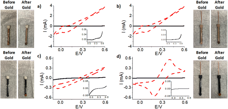
Conductive 3-D printing filaments have recently become available for FDM printers. Here, two different filaments were investigated, a Protopasta 1.75 mm Conductive PLA filament and a Multi3D 1.75 mm Electrifi Conductive Filament with resistivities of 115 Ω cm and 0.006 Ω cm respectively. For each of the filaments, two different chip designs were investigated with consistent measurements to ensure the surface area were consistent between different designs. EC optimization was performed concurrently with the chip design optimization. Overall, the conductivity of all four chip designs increased after gold deposition, as shown by an increase in current signal (red line). In Fig. 3a, where Multi3D filament was used, the current signal measured from the WE increased from 0.07 mA (black) to ≈4 mA (red) after gold deposition. This increase demonstrated that depositing gold on the surface of the electrode improves the conductivity of the electrode, although, proper ferri/ferrocyanide redox activity was not observed.26 Following, a Cu wire was embedded into the Multi3D filament, shown in Fig. 3b. This was done to determine if a better electrical connection between the electrode and potentiostat improves conductivity and/or improves the redox activity (not observed with this filament). Therefore, it was necessary to investigate a different conductive filament using Protopasta conductive PLA as shown in Fig. 3c. It is seen that the current increases from 0.02 mA (black) to 0.3 mA (red) after gold deposition which again confirms that gold increases the conductivity of the electrode surface, but limited redox activity was observed, as no typical ferri/ferrocyanide redox peak was observed.26 This limiting factor is likely due to insufficient electron flow from the WE to the electrical contacts connected to the potentiostat, resulting in poor electron flow and reduced conductivity in the CV plots. Therefore, a Cu wire was then embedded into this filament, shown in Fig. 3d, producing an increase in current from 0.005 mA (black) to 0.55 mA (red) after gold deposition. This resulted in a conductive WE for which typical EC redox activity of ferri/ferrocyanide redox was observed. Even though the Multi3D filament produced larger current values and higher conductivity, likely due to a variety of different elements that can increase conductivity as shown in Table S2,† when compared to the Protopasta filament. In addition, when using Multi3D filament, proper redox activity was not observed. Also, SEM and EDS results, shown in Fig. S5 and Table S2† respectively, showed that the Cu blend Multi3D filament absorbs the electrolyte thereby further altering the surface properties, and due to the Cu in the filament, could cause metal ion contamination. Therefore, it was determined that the most optimal chip design was when conductive Protopasta filament was used with an embedded copper wire as shown in Fig. 3d. With this design, it was necessary to optimize gold deposition parameters using chronoamperometry (CA).To obtain an optimal sensor with a stable gold layer on the electrode surface, CA was used on the optimal chip design using Protopasta conductive PLA filament with an embedded copper wire. Different potentials and deposition times applied to the WE result in different nucleation and growth mechanisms of gold deposited thereby further altering the conductivity of the electrode.27 Therefore, it was necessary to optimize the gold deposition potential and time to obtain a conductive chip.
Optimization of deposition potential
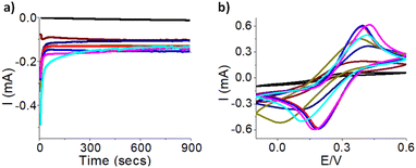
Studies have shown, the current from gold deposition increases negatively as potential becomes more negative, resulting in a more conductive electrode.27 To explore this further, CA was used and different potentials were investigated ranging from −0.2 V to −1.8 V while keeping gold deposition time constant at 15 minutes (Fig. 4a). As the potential became more negative, the deposition signal is nosier, a result which could be due to hydrogen evolution.28 CV's were then tested on each electrode to monitor the conductivity of the electrode by examining the current values (Fig. 4b). This figure shows that a CA deposition with a less negative potential of −0.2 V results in a smaller CV current but as the potential increases negatively towards −1.4 V, the current starts to increase indicating a more conductive electrode. Overall, the following deposition potentials of −1.4 V, −1.5 V and −1.6 V all resulted in a current value close to 0.6 mA, which appeared to be the largest current value. A deposition potential of −1.8 V did not increase the CV peak current value nor conductivity. The less conductive gold surface is likely due to hydrogen evolution and bubbling occurring on the WE, which results in the limiting diffusion of gold ions to the electrode surfaces.29 Since −1.4 V, −1.5 V, and −1.6 V potentials all resulted in similar current values shown on the CV in Fig. 4b, all three potentials were investigated to optimize gold deposition time.Optimization of deposition time
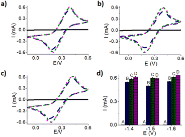
Using the three potentials that produced the highest current values in the CVs, different gold deposition times (Fig. 5) were investigated to obtain the optimal potential and time for gold deposition. Current increases were identified after depositing gold for 2 minutes shown in Fig. 5. Comparing 2 minutes deposition to 15 minutes, the current increased only slightly and a similar trend was observed for 30 minutes of gold deposition at potentials of −1.4 V and −1.6 V shown in Fig. 5a–c respectively. Observations of hydrogen evolution were made at different times over the three applied potentials. When a potential of −1.4 V was applied (Fig. 5a), hydrogen evolution did not occur after 2 or 15 minutes, but was apparent after 30 minutes. For −1.5 V (Fig. 5b), hydrogen evolution was observed after 15 minutes and for −1.6 V (Fig. 5c) it was noticed after 2 minutes. To look more closely at the differences, the oxidation peak current values (Table S3†) were all plotted with their respective error bars shown in Fig. 5d that were obtained from the oxidation peak values multiplied by relative percent standard deviation. Since it is important to avoid hydrogen evolution as it could potentially damage the electrode altering the performance and reproducibility of the electrodes,28–30 a gold deposition time of 15 minutes at a potential of −1.4 V was determined to be the most optimal for making sensor chips. In addition, a shorter gold deposition time while maintaining a quality deposition is important to move towards faster testing. Therefore, 15 minutes was chosen to be the preferred deposition time, although, a longer deposition time could give slightly more gold coating on the surface of the electrode. To ensure the gold deposition parameters were preferred, the reproducibility of the electrodes and gold stability were investigated.Reproducibility and stability of 3-D printed electrodes
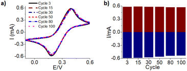
Multiple electrodes have been made to test out the reproducibility after controlling the surface area with epoxy glue as shown in Fig. S6 and Table S4.† The EC redox signal shows they are very similar but not identical. In addition, we tested the stability of gold deposition on the electrode surface. The most optimal gold deposition condition of −1.4 V for 15 minutes was used and then electrochemical cycling test with 100 CV cycles was carried out to ensure the current did not decrease as shown in Fig. 6a and b. Overall, comparison of cycle 3 to cycle 100 demonstrates a 1.8% and 9.2% decrease in the oxidation and reduction peak signal, respectively, calculated by relative percent change. This indicates the conductivity of the electrode remains relatively the same. These results represent that the 3-D printed electrode chips have stable gold surfaces. This is important if they are used in further applications such as chemical and biological sensing to ensure they maintain consistent performance.31Scanning electron microscopy and energy dispersive spectroscopy
To study the surface morphology and chemical composition of gold deposition, SEM and EDS was used. The topography of the PLA Protopasta 3-D printed electrode was imaged by SEM, shown in Fig. 7 with enlarged images in Fig. S7,† before and after gold deposition using a potential of −1.4 V over different total gold deposition times of 0, 2, 15, and 30 minutes (Fig. 7a, b, c and d respectively). Due to the 3-D printing process, the electrode surface was not perfectly smooth, but these rougher surfaces would enlarge the surface area and provide for more interactions of molecules when used in chemical and biosensing applications.14 When observing the surface over different deposition times, after 2 minutes clusters of gold could be observed on the surface of the electrode (inset Fig. 7b), but it had lower conductivity to be used in EC sensing. After a deposition of 15 minutes, the gold film becomes more prevalent and the clusters grow further increasing the conductivity, as shown in Fig. 7c. At 30 minutes of total gold deposition, the gold layer looked similar to that of the 15 minutes deposition time (Fig. 7d). The SEM images were analysed using Gwyddion software with threshold masking tool to quantify the percentage of gold cluster growth over different deposition times. The gold coverage ratio on the images was increased from 0% at 0 minute up to 30%, 64% and 81% after 2 minutes, 15 minutes, and 30 minutes of gold deposition respectively.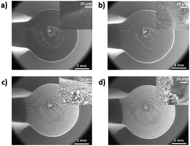 | ||
| Fig. 7 SEM images of Protopasta electrode with Cu wire embedded after gold deposition at −1.4 V potential over deposition times of (a) 0 minutes; (b) 2 minutes; (c) 15 minutes; (d) 30 minutes. | ||
EDS measurements, on the same electrode, were collected to observe the amount of gold deposited at the different time intervals (Table 1). There is an overall trend of increasing the amount of gold on the electrode with increasing deposition time. However, beyond 15 minutes the rate of deposition slows similar to the resulting CV current measurements (Table S3†).
| Carbon (%) | Oxygen (%) | Gold (%) | |
|---|---|---|---|
| 0 min | 76.8 | 23.2 | 0.00 |
| 2 min | 70.4 | 28.6 | 1.03 |
| 15 min | 73.2 | 20.5 | 6.33 |
| 30 min | 73.9 | 19.4 | 6.72 |
SEM images were also taken on electrodes that had gold deposited over 15 minutes while varying the potentials (−0.6 V, −1.0 V, −1.4 V, and −1.8 V) as shown in Fig. S8.† SEM images showed gold grain size and density change with varying electrodeposition potentials. Gold grains look to be smaller with increasing potentials from −0.6 V to −1.8 V. Gold deposition at the optimized potential of −1.4 V gives a good combination of coverage, size and growth of the gold layer.
X-ray photoelectron spectroscopy (XPS)
To further study the electrodes surface chemistry, including the chemical state of the atoms and what oxidation state gold is being electrodeposited at, XPS measurements were conducted on the Protopasta electrode after gold deposition with the experimental details in SI. Overall, strong peaks were observed for Carbon, Oxygen and Gold as shown in Fig. S9† with its corresponding data in Table S5.† In the high resolution spectrum of Au 4f, only the presence of Au-0 (Au 4f7/2 at 83.87 eV and Au 4f5/2 at 87.54 eV) was detected. Au+1 and Au+3 was not observed as this would occur with a shift to higher binding energies by 1.1 and 3.2 eV from 83.87 eV respectively.32,33 This analysis demonstrated that the gold that is electrodeposited onto the surfaces of the electrodes is indeed Au(0).Extension to practical sensing of Cu2+
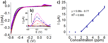
To demonstrate the applicability of the 3-D printed electrode to practical applications the fabricated sensors and ASV technique was used to measure Cu2+ with ppm (μg mL−1) limit of detection (LOD). Although Cu is an essential element to humans and plants, excess amounts of Cu is toxic to biological systems.34–36 The detection and quantification of Cu in the environment are important, especially due to the wide industrial usage of Cu.37,38 Although there are several established conventional methods (e.g. inductively coupled plasma mass spectrometry; colourimetric methods) that detect Cu at levels practical for environmental regulations, there has been significant interest in developing electroanalytical methods for the rapid and online detection of Cu.39,40 Cu in drinking water presents in various forms. The EC analysis of Cu2+ was explored, due to its soluble, bioavailable nature and relevance to toxicological standpoint.38 Prior to detecting Cu2+, the electrodes were electrochemically cleaned by CV in 0.5 M H2SO4. The electrochemical cleaning did not largely affect the surface of the electrode. SEM and EDS analysis shows a small 2% increase was observed for gold composition as shown in Fig. S10 and Table S6.† The Cu2+ oxidation peak collected by ASV demonstrated an increased current at higher Cu concentrations (Fig. 8a and b). The background has been subtracted from Fig. 8a to remove the contribution of oxygen evolution that may occur and to accurately measure the pure faradaic current that is obtained in Fig. 8b.41 The peak current values (n = 3) of Cu2+ after background subtraction were used to generate a linear calibration curve between 2 to 6 ppm, as shown in Fig. 8c, matching the concentration level of regulation guidelines. A LOD of 1.6 ppm was obtained from 7 replicated measurements of the blank using 3σ/slope, where σ is standard deviation. When detection was carried out at LOD level and lower, the faradaic current from the detection is at a very similar level to the background non-faradaic current, therefore is difficult to be recognized. Ziba et al. used a carbon ionic liquid electrode to detect trace Cu2+ with a LOD of 5.97 × 10⁻⁴ ppm.42 While their detection showed very high sensitivity, the work shown is to illustrate a new possible way of making the electrode cheaply and locally. Future studies in electrode modification materials have potential to further improve the performance of these 3-D printed electrodes. The LOD calculated is close to the Canadian drinking water guideline value of copper (maximum acceptable concentration of 2 ppm and aesthetic objective of 1 ppm),38 the USEPA has a maximum contaminant level of 1.3 ppm,43 and the World Health Organization has a guideline value of 2 ppm,44 which suggests that the 3-D printed electrode may readily detect Cu2+ at threshold concentrations. The 3-D printed electrodes were also tested against other interfering ions, shown in Fig. S11,† and it was determined that the interfering ions had no significant impact on the detection of Cu2+ according to the statistical t-test.Conclusions
We have illustrated the use of electrochemically depositing gold on the surface of 3-D printed electrodes to improve conductivity and EC sensing of Cu2+. To ensure good conductivity and proper redox activity, Protopasta conductive PLA filament with an embedded Cu wire was found to provide the best performance for the fabricated chip design. This design ensures no possibility of metal contamination in the filament and a good, stable connection between the electrode and potentiometer. Chronoamperometry proved successful for EC gold deposition, with an increase in CV current with increasing deposition time. The current method results in quick, accessible, and low-cost fabricated chips since no nanofabrication facility is required for gold deposition and it results in less gold waste when compared to methods that involve vaporizing gold onto the substrate. Cyclic voltammetry demonstrated that the electrodes are conductive, especially after gold deposition affording the opportunity to use the electrodes for chemical and biological sensing applications. The geometry of the chips is easily customizable with CAD software to tailor any sensor design. Detection of Cu2+ at ppm concentrations was successfully demonstrated proving the fabricated electrode can function as a sensor and be further improved for future applications. Furthermore, this electrode fabrication method has the potential to be implemented in other applications, such as electronics, electrochemistry, and biosensors.45–48Author contributions
KP and ZS formulated ideas of overarching research goals and developed the experiment strategies. KP has carried out 3-D printing, electrochemical investigation, data analysis and writing initial version of manuscript. PH and MH assisted with designs with 3-D software and building 3-D printers. RO provided expertise in 3-D printing techniques and material selections. YP and SJP provided expertise in Cu2+ metal detection while YP conducted experiments. KM conducted SEM and EDS experiments. GS conducted XPS experiments. All co-authors reviewed and edited the manuscript.Conflicts of interest
There are no conflicts to declare.Acknowledgements
ZS, RO, SJP would like to acknowledge Natural Sciences and Engineering Research Council of Canada (NSERC) for support through the Discovery and Alliance program and the Canada Foundation for Innovation (CFI) for infrastructure support. The authors would like to acknowledge the Queen's Chemistry Microscopy Facility for access to the electron microscopes.Notes and references
- Organization for Economic Co-operation and Development, Testing for COVID-19- A way to lift confinement restrictions, 2020 Search PubMed.
- H. Karimi-Maleh, F. Karimi, M. Alizadeh and A. L. Sanati, Electrochemical Sensors, a Bright Future in the Fabrication of Portable Kits in Analytical Systems, Chem. Rec., 2020, 20(7), 682–692 CrossRef.
- A. M. Nelson, S. Habibi, J. Lee and M. A. Burns, Electrochemical Deposition of Lead for Water Quality Sensing, J. Electrochem. Soc., 2022, 169, 017505 CrossRef.
- M. A. Mohammad Haniff, S. Muhammad Hafiz, K. A. Wahid, Z. Endut, H. Wah Lee, D. C. Bien, I. Abdul Azid, M. Z. Abdullah, N. Ming Huang and S. Abdul Rahman, Piezoresistive effects in controllable defective HFTCVD graphene-based flexible pressure sensor, Sci. Rep., 2015, 5, 14751 CrossRef PubMed.
- K. Scholten and E. Meng, Electron-beam lithography for polymer bioMEMS with submicron features, Microsyst. Nanoeng., 2016, 2, 16053 CrossRef.
- J. Yan, V. A. Pedrosa, A. L. Simonian and A. Revzin, Immobilizing enzymes onto electrode arrays by hydrogel photolithography to fabricate multi-analyte electrochemical biosensors, ACS Appl. Mater. Interfaces, 2010, 2(3), 748–755 CrossRef PubMed.
- B. L. McIntyre and C. L. Dennis, Low-cost electron-beam lithography package for the scanning electron microscope, Appl. Opt., 1988, 27(2), 196 CrossRef.
- H. S. Jeong, S. Hwang, K. S. Min and S. B. Jun, Fabrication of Planar Microelectrode Array Using Laser-Patterned ITO and SU-8, Micromachines, 2021, 12, 1347 CrossRef.
- M. Keough, J. F. McLeod, T. Salomons, P. Hillen, Y. Pei, G. Gibson, K. McEleney, R. Oleschuk and Z. She, Realizing new designs of multiplexed electrode chips by 3-D printed masks, RSC Adv., 2021, 11(35), 21600–21606 RSC.
- E. Costa-Rama and M. T. Fernandez-Abedul, Paper-Based Screen-Printed Electrodes: A New Generation of Low-Cost Electroanalytical Platforms, Biosensors, 2021, 11, 51 CrossRef.
- Z. Taleat, A. Khoshroo and M. Mazloum-Ardakani, Screen-printed electrodes for biosensing: a review (2008–2013), Microchim. Acta, 2014, 181(9–10), 865–891 CrossRef CAS.
- G. Alberti, C. Zanoni, S. Rovertoni, L. R. Magnaghi and R. Biesuz, Screen-Printed Gold Electrode Functionalized with Deferoxamine for Iron(III) Detection, Chemosensors, 2022, 10, 214 CrossRef CAS.
- F. Kuralay, S. Campuzano, D. A. Haake and J. Wang, Highly sensitive disposable nucleic acid biosensors for direct bioelectronic detection in raw biological samples, Talanta, 2011, 85(3), 1330–1337 CrossRef CAS PubMed.
- J. E. Contreras-Naranjo, V. H. Perez-Gonzalez, M. A. Mata-Gómez and O. Aguilar, 3D-printed hybrid-carbon-based electrodes for electroanalytical sensing applications, Electrochem. Commun., 2021, 130 Search PubMed.
- G. Martins, J. L. Gogola, L. H. Budni, B. C. Janegitz, L. H. Marcolino-Junior and M. F. Bergamini, 3D-printed electrode as a new platform for electrochemical immunosensors for virus detection, Anal. Chim. Acta, 2021, 1147, 30–37 CrossRef CAS PubMed.
- D. Peng, B. Hu, M. Kang, M. Wang, L. He, Z. Zhang and S. Fang, Electrochemical sensors based on gold nanoparticles modified with rhodamine B hydrazide to sensitively detect Cu(II), Appl. Surf. Sci., 2016, 390, 422–429 CrossRef CAS.
- J. J. A. Gómez, C. Zubieta, R. M. Ferullo and S. G. García, Electrochemical formation and characterization of Au nanostructures on a highly ordered pyrolytic graphite surface, Appl. Surf. Sci., 2016, 363, 356–362 CrossRef.
- N. German, A. Ramanavicius and A. Ramanaviciene, Electrochemical deposition of gold nanoparticles on graphite rod for glucose biosensing, Sens. Actuators, B, 2014, 203, 25–34 CrossRef.
- S. Liu, D. Leech and H. Ju, Application of Colloidal Gold in Protein Immobilization, Electron Transfer, and Biosensing, Anal. Lett., 2003, 36(1), 1–19 CrossRef.
- Yi Xiao, F. P. E. Katz, J. F. Hainfeld and I. Willner, “Plugging into enzymes”-nanowiring of redox enzymes by a gold nanoparticle, Science, 2003, 299(5614), 1877–1881 CrossRef PubMed.
- A. Galal, N. F. Atta and E. H. El-Ads, Probing cysteine self-assembled monolayers over gold nanoparticles-towards selective electrochemical sensors, Talanta, 2012, 93, 264–273 CrossRef PubMed.
- P. Bollella, Porous Gold: A New Frontier for Enzyme-Based Electrodes, Nanomaterials, 2020, 10, 722 CrossRef CAS.
- J. McLeod, C. Park, A. Cunningham, L. O'Donnell, R. S. Brown, F. Kelly and Z. She, Developing a toll-like receptor biosensor for Gram-positive bacterial detection and its storage strategies, Analyst, 2020, 145(18), 6024–6031 RSC.
- I. H. Cho, D. H. Kim and S. Park, Electrochemical biosensors: perspective on functional nanomaterials for on-site analysis, Biomater. Res., 2020, 24, 6 CrossRef.
- D. V. Baker, C. Bao and W. S. Kim, Highly Conductive 3D Printable Materials for 3D Structural Electronics, ACS Appl. Electron. Mater., 2021, 3(6), 2423–2433 CrossRef.
- P. Krishnaveni and V. Ganesh, Electron transfer studies of a conventional redox probe in human sweat and saliva bio-mimicking conditions, Sci. Rep., 2021, 11(1), 7663 CrossRef.
- Y. G. Li and A. Lasia, Nucleation and crystal growth in gold electrodeposition from acid solution Part II- Hard gold, Appl. Electrochem., 1996, 26, 853–863 CrossRef.
- Y. B. Vogel, N. Darwish, M. B. Kashi, J. J. Gooding and S. Ciampi, Hydrogen evolution during the electrodeposition of gold nanoparticles at Si(100) photoelectrodes impairs the analysis of current-time transients, Electrochim. Acta, 2017, 247, 200–206 CrossRef.
- Y. B. Vogel, C. W. Evans, M. Belotti, L. Xu, I. C. Russell, L. J. Yu, A. K. K. Fung, N. S. Hill, N. Darwish, V. R. Goncales, M. L. Coote, K. Swaminathan Iyer and S. Ciampi, The corona of a surface bubble promotes electrochemical reactions, Nat. Commun., 2020, 11(1), 6323 CrossRef.
- X. Zhao, H. Ren and L. Luo, Gas Bubbles in Electrochemical Gas Evolution Reactions, Langmuir, 2019, 35(16), 5392–5408 CrossRef PubMed.
- R. Khadka, N. Aydemir, C. Carraher, C. Hamiaux, P. Baek, J. Cheema, A. Kralicek and J. Travas-Sejdic, Investigating Electrochemical Stability and Reliability of Gold Electrode-electrolyte Systems to Develop Bioelectronic Nose Using Insect Olfactory Receptor, Electroanalysis, 2019, 31(4), 726–738 CrossRef.
- M. T. Camci, B. Ulgut, C. Kocabas and S. Suzer, In-Situ XPS Monitoring and Characterization of Electrochemically Prepared Au Nanoparticles in an Ionic Liquid, ACS Omega, 2017, 2(2), 478–486 CrossRef PubMed.
- J. Lee and M. Lee, Laser-Induced Conversion of Au Powders to Highly Stable Nanoparticles with a Narrow Size Distribution, J. Phys. Chem. C, 2016, 120(24), 13256–13262 CrossRef.
- O. Bandmann, K. H. Weiss and S. G. Kaler, Wilson’s disease and other neurological copper disorders, Lancet Neurol., 2015, 14, 103–113 CrossRef.
- M. Araya, M. Olivares, F. Pizarro, A. Llanos, G. Figueroa and R. Uauy, Community-based randomized double-blind study of gastrointestinal effects and copper exposure in drinking water, Environ. Health Perspect., 2004, 112(10), 1068–1073 CrossRef.
- M. Araya, M. C. McGoldrick, L. M. Klevay, J. J. Strain, P. Robson, F. Nielsen, M. Olivares, F. Pizarro, L. A. Johnson and K. A. Poirier, Determination of an acute no-observed-adverse-effect level (NOAEL) for copper in water, Regul. Toxicol. Pharmacol., 2001, 34(2), 137–145 CrossRef PubMed.
- E. Bernalte, S. Arévalo, J. Pérez-Taborda, J. Wenk, P. Estrela, A. Avila and M. Di Lorenzo, Rapid and on-site simultaneous electrochemical detection of copper, lead and mercury in the Amazon river, Sens. Actuators, B, 2020, 307 Search PubMed.
- Health Canada. Guidelines for Canadian Drinking Water Quality, Copper. 2019 Search PubMed.
- S. Cinti, V. Mazzaracchio, G. Ozturk, D. Moscone and F. Arduini, A lab-on-a-tip approach to make electroanalysis user-friendly and de-centralized: Detection of copper ions in river water, Anal. Chim. Acta, 2018, 1029, 1–7 CrossRef PubMed.
- E. Ç. Canpolat, E. Şar, N. Y. Coşkun and H. Cankurtaran, Determination of Trace Amounts of Copper in Tap Water Samples with a Calix[4]arene Modified Carbon Paste Electrode by Differential Pulse Anodic Stripping Voltammetry, Electroanalysis, 2007, 19(10), 1109–1115 CrossRef.
- L. Kryger and J. Daniel, Part II. Multiple Scanning and Background Subtraction. A New Technique for Strpiping Analysis, Comput. Electroanal., 1975, 78, 251–260 Search PubMed.
- Z. Karimi, S. Mojtaba and A. Besharati-Seidani, Electrochemical Determination of Trace Cu2+ in Water Samples by Using Carbon Ionic Liquid Electrode Modified with Molecularly Imprinted Polymers, Adv. Nanochem., 2021, 3(2), 49–55 Search PubMed.
- United States Environmental Protection Agency, National Primary Drinking Water Regulations, 2009 Search PubMed.
- World Health Organization, Guildelines for Drinking-water Quality: fourth edition incorporating the first addendum, 2017, p. 188 Search PubMed.
- E. Sardini, M. Serpelloni and S. Tonello, Printed Electrochemical Biosensors: Opportunities and Metrological Challenges, Biosensors, 2020, 10, 0166 CrossRef.
- C. Y. Foo, H. N. Lim, M. A. Mahdi, M. H. Wahid and N. M. Huang, Three-Dimensional Printed Electrode and Its Novel Applications in Electronic Devices, Sci. Rep., 2018, 8(1), 7399 CrossRef PubMed.
- G. Remaggi, A. Zaccarelli and L. Elviri, 3D Printing Technologies in Biosensors Production: Recent Developments, Chemosensors, 2022, 10, 65 CrossRef.
- M. P. Browne, F. Novotny, Z. Sofer and M. Pumera, 3D Printed Graphene Electrodes' Electrochemical Activation, ACS Appl. Mater. Interfaces, 2018, 10(46), 40294–40301 CrossRef PubMed.
Footnote |
| † Electronic supplementary information (ESI) available. See DOI: https://doi.org/10.1039/d2ra05455h |
| This journal is © The Royal Society of Chemistry 2022 |

