DOI:
10.1039/D2RA05484A
(Paper)
RSC Adv., 2022,
12, 30157-30166
Self-biased photodetector using 2D layered bismuth triiodide (BiI3) prepared using the spin coating method
Received
31st August 2022
, Accepted 8th October 2022
First published on 21st October 2022
Abstract
Layered bismuth triiodide (BiI3) is a 2D material that has emerged as an ideal choice for optical sensors. Although BiI3 has been prepared using vacuum-based deposition techniques, there is a dearth of research studies on synthesizing this material using chemical route. The present work uses a facile spin coating method with varying rotation speeds (rpm) to fabricate BiI3 material thin films for photodetection applications. The structural, optical, and morphological study of BiI3 thin films prepared at 3000–6000 rpm were investigated. XRD analysis indicates formation of BiI3 films and revealed that BiI3 has a rhombohedral crystal structure. FESEM analysis showed that BiI3 films prepared at different rpm are homogeneous, dense, and free from cracks, flaws, and protrusions. In addition, films show an island-like morphology with grain boundaries having different grain sizes, micro gaps, and the evolution of the granular morphology of BiI3 particles. The UV spectroscopy and photoluminescence analysis revealed that BiI3 films strongly absorb light in the visible region of spectra with a high absorption coefficient of ∼104 cm−1, have an optical band gap of ∼1.51 eV. A photodetector was realised using fabricated BiI3 film obtained at an optimum spin speed of 4000 rpm. It showed rapid rise and decay times of 0.4 s and 0.5 s, a responsivity of ∼100 μA W−1, external quantum efficiency of 2.1 × 10⁻⁴%, and detectivity of ∼3.69 × 10⁶ Jones at a bias voltage of 0 V. Our results point towards a new direction for layered 2D BiI3 materials for the application in self-biased photodetectors.
1. Introduction
Photodetector is an optoelectronic device that converts optical signals into electrical signals. It works on the principle of photoelectric effect i.e. when photons strike the material, it absorbs energy and generates electron–hole pairs (EHPs), thereby forming excitons. In this information era, photodetectors have become indispensable devices due to their application in optical communication and optoelectronics. In the last two decades, many new materials have been discovered with remarkable optical and electronic properties to realize photodetectors having application in optical communication, image sensing, night surveillance, environmental monitoring, and biological/chemical detection.1–5 The most popular materials employed for photodetection are crystalline inorganic semiconductors like Si, InGaAs, GaN, etc. These materials have outstanding charge carrier mobility, high stability, and small exciton binding energy.6,7 These material-based photodetectors have limitations in practical applications due to their high operating voltage, mechanical inflexibility, complex and expensive manufacturing process, and low driving temperature. Therefore, researchers are looking for several other materials to overcome these limitations, such as 2D layered graphene, transition metal dichalcogenides (for example, WS2 and MoS2), metal chalcogenides (such as InS2 and InSe), and metal halides (such as PbI2 and BiI3). Photodetectors based on these materials have shown extraordinary detection capability over a broad spectrum ranging from UV to IR.8–12 Apart from these 2D materials, flexible devices based on organic, inorganic Pb hybrid perovskite materials such as MAPbBr3,13 α-CsPbI3,14,15 have shown extraordinary rectifying performance. Li et al.16 have reported excellent stability of over 1 year in the synthesized material. Despite such significant advancement, there are still challenges that needs to be addressed such as Pb toxicity and stability, which are critical issues in practical applications.17 To overcome these issues, trials are being undertaken in which organic cation is replaced with inorganic one, replacing divalent lead with other materials such as Ge, Sn, Cu, Fe, Pd, Mn, Sb, and Bi. Among these, Sn and Ge have stability issues, as they easily get oxidized due to low binding energy. Bi3+ and Sb3+ have features similar to Pb2+, like same electronegativity and ionic radius.17 Among all replacements, Bi-based compounds offer great promising properties and they have been scarcely explored.18 Therefore, to advance perovskite materials for their reliable, practical applications, the present work aims to analyze the substitutional Bi-based material, prominently bismuth triiodide (BiI3) for self biased photodetector application.
BiI3 is a favorable 2-D layered material from the metal halides family. It exhibits a repeating unit of sandwiched I–Bi–I layers with strong Bi–I ionic bonds in mono layers and weak van der Waals interactions between them.19 The unique properties include a wide bandgap of 1.67 eV,20 high dielectric constant,21 high electron mobility (260 ± 50 cm2 V−1 s−1)22 or 1000 ± 200 with Sb doping,23 make it an attractive material for next-generation photonic and optoelectronic devices. The material has been successfully employed for solar photovoltaics,24 laser CUT-OFF applications,25 nuclear radiation detectors,26 X-ray detection,27,28 nanoscale pressure sensors,29 and photocatalytic applications,30 etc.
Various methods have been used to prepare BiI3, which includes physical vapor deposition (PVD),31 hydrothermal method,32 hot wall technique33 and thermal evaporation.34 Different morphologies such as 1-D, 2-D, and 3-D nanoparticles/nanosheets of BiI3 can be obtained using above listed methods.35,36 However, these synthesis techniques require high processing temperature, costly equipment, and coherent processing is time-consuming. Furthermore, their high processing temperature limits their practical applications in flexible, large-area, low-cost portable devices. On the other hand, a one-step solution-based method such as spin coating is widely adopted for synthesizing high-quality films due to its easy and time-saving process.37 Apart from this, spin coating has various advantages, such as low-temperature processes, requirement of low-cost precursors, and it is environmental benign and safe. Due to closed reaction processes, better stoichiometry is achieved and by controlling process parameters one can control morphology and particle size. Furthermore, it does not require any seed-catalyst and expensive surfactant.
Herein the study focuses on photodetector fabrication using a simple and inexpensive one-step solution-processed spin coating method. Bismuth iodide(III) (BiI3) thin films were used in afore-mentioned photodetector, which were annealed at 160 °C for 45 min. Furthermore, the effect of spin speed on the structural, morphological, and optical properties of BiI3 thin films was investigated. Finally, at an optimized spin speed (4000 rpm), BiI3-based photodetectors were directly fabricated on FTO substrates. The fabricated photodetector shows stable photoswitching behavior, remarkable detectivity and photoresponsivity, and rapid response with fast recovery times. The present work demonstrates that BiI3 has great potential for photodetector applications.
2. Experiment
2.1. Preparation of the electron transport layer (ETL)
An electron transport layer (ETL) compact TiO2 was deposited on FTO substrate by RF sputtering technique. A four-inch target of TiO2 (99.99%, VIN Karola) was used for TiO2 film deposition. First, the substrates were sequentially cleaned with soap water, isopropyl alcohol, ethanol, and distilled water in an ultrasonicated bath for 10 min each. Then, substrates were loaded onto a substrate holder, and the deposition system was evacuated to a back pressure of 1 × 10⁻⁸ mbar. Compact TiO2 films were deposited by maintaining the deposition parameters at 4 × 10⁻² mbar with constant 150 W RF power for 2 h. The prepared TiO2 films were subsequently annealed at a temperature of 400 °C for 1 h.
2.2. Preparation of BiI3 thin films
Metal halide BiI3 thin films were prepared at room temperature in an ambient atmosphere by the spin coating deposition technique. In this experiment, we have used (BiI3) and N,N-dimethylformamide (DMF) as chemical precursor and solvent, respectively. To synthesize the solution of BiI3, 1 molar BiI3 was added to 1 ml DMF and stirred for 2.5 h without heat treatment. Before deposition, the mixed solution was filtered with a PTAA-0.45 μm filter. Then, this filtered solution was used in the spin coating method to prepare BiI3 thin films on the RF-sputtered c-TiO2 films. The spin speed was varied from 3000 rpm to 6000 rpm in the steps of 1000 rpm. Other parameters, such as spin time and concentration of the solution, were kept constant. Afterwards, the deposited films were heated at 160 °C for 45 min on a hot plate in an ambient atmosphere. Finally, the films were allowed to cool to room temperature. Fig. 1 represents the synthesis protocol adapted for realization of BiI3 thin films.
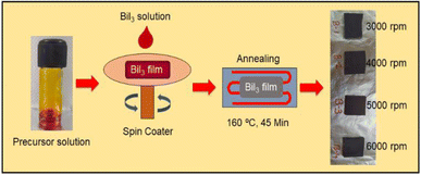 |
| | Fig. 1 Synthesis protocol for BiI3 thin films. | |
2.3. Device fabrication and photoresponse measurements
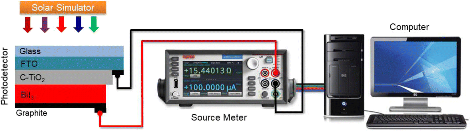
The device fabrication approach is divided into two steps. In the first step, we deposited BiI3 layer on FTO/compact-TiO2 by spin coating. Then in the second step, we deposited graphite on FTO/compact-TiO2/BiI3 as a bottom contact of the device for charge extraction using simple doctor blade method. The graphite paste was prepared by adding isopropyl alcohol (IPA) solution to graphite powder. Fig. 2 shows the device schematics for the BiI3-based photodetector and photoresponse measurement setup. The photoresponse measurements of prepared BiI3 films were conducted using a Keithley 2450 source-meter connected to the computer. White light illumination was performed via a solar simulator (ORIEL SOL 2A 94022A Class ABA). Time-dependent photoswitching studies were measured under standard AM 1.5 sunlight (100 mW cm−2) with zero bias applied voltage at room temperature. The effective area of the photodetector used was 2 cm2.
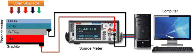 |
| | Fig. 2 Schematic of the photodetector and its properties measurement setup. | |
2.4. Characterization
The X-ray diffraction analysis was recorded with Cu-Kα radiation (λ ∼ 15.4 nm) using a Bruker D8 Advance diffractometer (Germany) in the 2θ = 10° to 60°. The UV-Visible-NIR spectrophotometer (JASCO, V-670) was used for the optical properties study. The absorption spectra were recorded between the wavelength of 200 nm to 800 nm. The photoluminescence spectra were recorded on a Fluorolog HORIBA Jobin Yvon spectrophotometer. Morphological micrographs were taken with different magnifications by an FEI Nova NanoSEM 450 microscope. The thickness of all the fabricated BiI3 thin films was measured by the Dektak XT Bruker profilometer.
3. Results and discussion
3.1. Variation in thickness
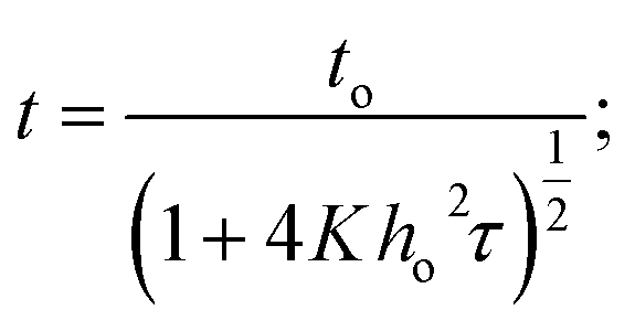
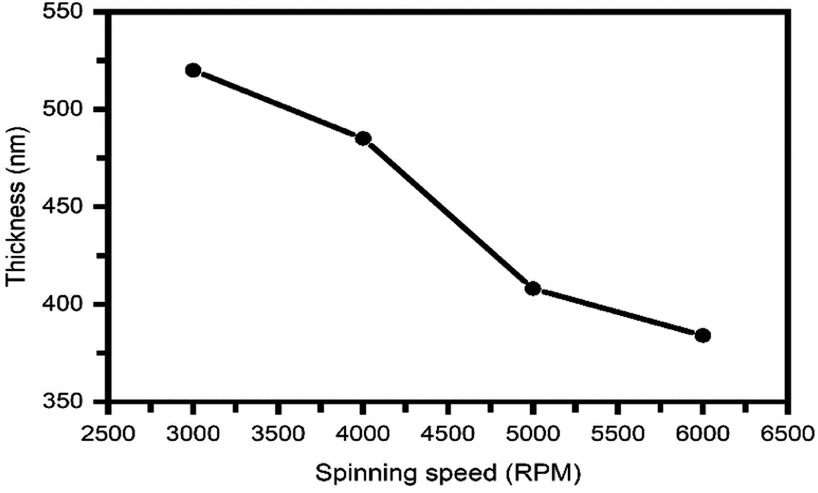
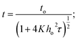
Fig. 3 shows the variation of BiI3 film thickness as a function of the spin speed. As expected, the thickness of the BiI3 film decreases with an increase in spin speed. It drops from 520 nm to 384 nm as the spin speed is increased from 3000 to 6000 rpm. In this spin coating technique, the thickness (t) of the film is defined by equation,38| |
 | (1) |
where to is the film thickness at the initial liquid, τ is the spin duration, and K is the system constant represented by K = ρω2/3η, where ρ indicates the liquid density, ω represents the spin speed, and η denotes the liquid viscosity. Thus, if the spin duration is constant for a specified precursor, then the thickness of the film decreases as the spin speed increases.
 |
| | Fig. 3 Variation in film thickness as a function of the spin speed of BiI3 films. | |
3.2. Structural analysis
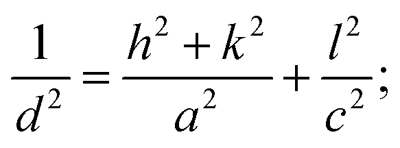
The formation of BiI3 thin film was confirmed through XRD analysis. Fig. 4 shows the XRD pattern of BiI3 thin films deposited on FTO by spin coating at different spin speeds. The XRD pattern of FTO is also incorporated in Fig. 4, and the peaks labeled with asterisks (*) correspond to the FTO substrate. The appearance of multiple peaks in the XRD pattern indicates polycrystalline nature of the films. The major diffraction peaks are observed at 2θ ∼ 12.6°, 13.5°, 25.5°, 26.8°, 35.1°, 41.5°, 43.6°, 46.1°, 54.5°, and 58.1°, which correspond to the (003), (101), (006), (113), (211), (300), (208), (119), (226), and (309) crystal planes, respectively, of the rhombohedral crystal structure of BiI3 with space group R![[3 with combining macron]](https://www.rsc.org/images/entities/char_0033_0304.gif) . It is observed that as spin speed increases, the preferred orientation of BiI3 crystallites changes from (003) to (113). All the peaks are well-matched with the standard diffraction pattern of BiI3 (JCPDS data card # 48-1795). The inter-planar spacing between atoms (d-spacing) for BiI3 films at different spin speeds is determined by Bragg's law,
. It is observed that as spin speed increases, the preferred orientation of BiI3 crystallites changes from (003) to (113). All the peaks are well-matched with the standard diffraction pattern of BiI3 (JCPDS data card # 48-1795). The inter-planar spacing between atoms (d-spacing) for BiI3 films at different spin speeds is determined by Bragg's law,| |
2d![[thin space (1/6-em)]](https://www.rsc.org/images/entities/char_2009.gif) sinθ = nλ; sinθ = nλ;
| (2) |
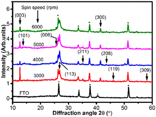 |
| | Fig. 4 XRD pattern of BiI3 films deposited spin coating at different spin speeds. | |
The observed interplanar spacing value of the BiI3 film is 3.32 Å, which is in agreement with the previously reported d-value (3.38 Å) of bulk BiI3.39 These results confirmed the formation of BiI3 thin films by a cost-effective and single-step spin coating method. The lattice parameters (a, b, and c) and the unit-cell volume (V) of BiI3 films were calculated by using,40
| |
 | (3) |
The obtained values of lattice constants are a ∼ 5.327 Å, c ∼ 21.051 Å and V = 597.36 Å3. These values match well with previously reported data,41–43 further confirming the formation of BiI3 films. The average grain size (dX-ray) of BiI3 films was determined from the (003)/(113) plane located at 2θ ∼ 12.06°/26.8° using Debye–Scherrer's equation,44
| |
 | (5) |
where
λ indicates the wavelength,
β represents full width at half maximum (FWHM), and
θ represents Bragg's diffraction angle. As seen in
Table 1, the average grain size does not show any particular trend with increased spin speed. However, the BiI
3 thin film prepared at 4000 rpm has the largest grain size.
Table 1 Microstructural parameters of BiI3 films prepared at different spin speeds
| Spin speed (rpm) |
dX-ray (nm) |
Preferred orientation |
Degree of crystallinity (%) |
ε (10−3) |
δ × 1014 (line per m2) |
α (10−3) |
Texture coefficient (TC) |
| (003) |
(113) |
| 3000 |
58 |
(003) |
46 |
2.2 |
2.97 |
1.82 |
1.14 |
0.76 |
| 4000 |
68 |
(113) |
63 |
1.3 |
2.16 |
1.08 |
0.54 |
1.28 |
| 5000 |
54 |
(113) |
59 |
1.5 |
3.43 |
1.36 |
0.74 |
1.10 |
| 6000 |
26 |
(113) |
56 |
1.4 |
14.8 |
2.83 |
0.61 |
0.96 |
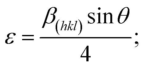
To examine the effect of spin speed on the microstructural properties of BiI3 films, we have calculated the dislocation density, microstrain, stacking fault probability, degree of crystallinity, texture coefficients, etc. These values are listed in Table 1. The crystal structure of BiI3 is a layered 2-D material built from BiI6 octahedra with 1/3 of the vacant cation sites. It has been reported that each unit cell of BiI3 contains three stacked I–Bi–I layers, and in each layer, three closed-pack atomic sheets are stacked in the I–Bi–I sequence.45 As a result, faults in stacking are generally found in BiI3 crystals.46,47 These crystal imperfections and distortions induce microstrain (ε) in the film, which is given by,48
| |
 | (6) |
The calculated microstrain values for BiI3 film are shown in Table 1. The lowest microstrain was observed for the BiI3 film prepared at 4000 rpm. The microstrain in the film depends on the grain boundaries of the crystallites.49 The grain size reduces the grain boundaries, hence the microstrain in the film.
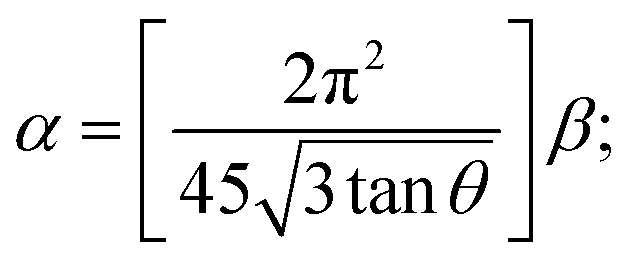
The stacking fault probability (α) is the fraction of layers that undergoes sequential stacking faults in a crystal50 and can be measured by,51
| |
 | (7) |
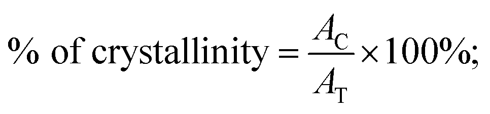
Among all prepared BiI3 thin films, the lowest stacking fault density was observed for the 4000 rpm sample, implying improved crystallinity. Sometimes, the crystalline peaks overlap with the amorphous hump in the XRD pattern. The crystalline phase can be calculated based on the percentage of crystallinity. Also, it can be calculated by the crystalline XRD peak integrated over the area divided by the film's total integrated area in the XRD pattern.52
| |
 | (8) |
where
AC is the crystalline XRD peak integrated area and
AT is the total integrated area of the XRD pattern. The degree of crystallinity critically depends on the spin speed. The highest crystallinity degree (63%) is observed for the BiI
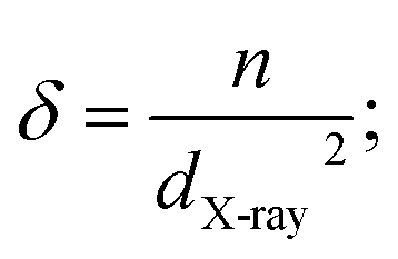
3 film prepared at 4000 rpm. The material properties are strongly influenced by the dislocation/crystallographic defect or irregularity within a crystal structure. The dislocation density (
δ) is the length of dislocation lines per unit volume of the crystal and was determined by using the following relation,
53| |
 | (9) |
where
n represents the factor equal to unity for the minimum dislocation density and
dX-ray is the crystallite size. The lowest dislocation density of 1.08 × 10
−3 was obtained for the BiI
3 thin film prepared at 4000 rpm.
To examine the effect of spin speed on the preferential orientation of crystallites along the (hkl) plane in the film, the texture coefficient [(TC)hkl] was calculated. It is calculated using,54,55
| |
 | (10) |
where
Ii is the relative intensity,
Io indicates the integral intensity of the JCPDS data (powder diffraction pattern) of the corresponding plane
i, and
N represents the number of reflections in the XRD pattern. If the TC
(hkl) value is equal to 1 that means no preferred orientation,
56 whereas a TC greater than 1 indicates the preferred orientation of the crystallites in that particular direction.
57 The calculated values of the texture coefficients are shown in
Table 1. The BiI
3 thin films prepared at 3000 and 4000 rpm has texture coefficients 1.14 and 1.28 for the (003) and (113) planes. These results suggest that as the spin speed changes from lower to higher values, the orientation changes from the (003) direction to the (113) direction.
3.3. Morphological analysis
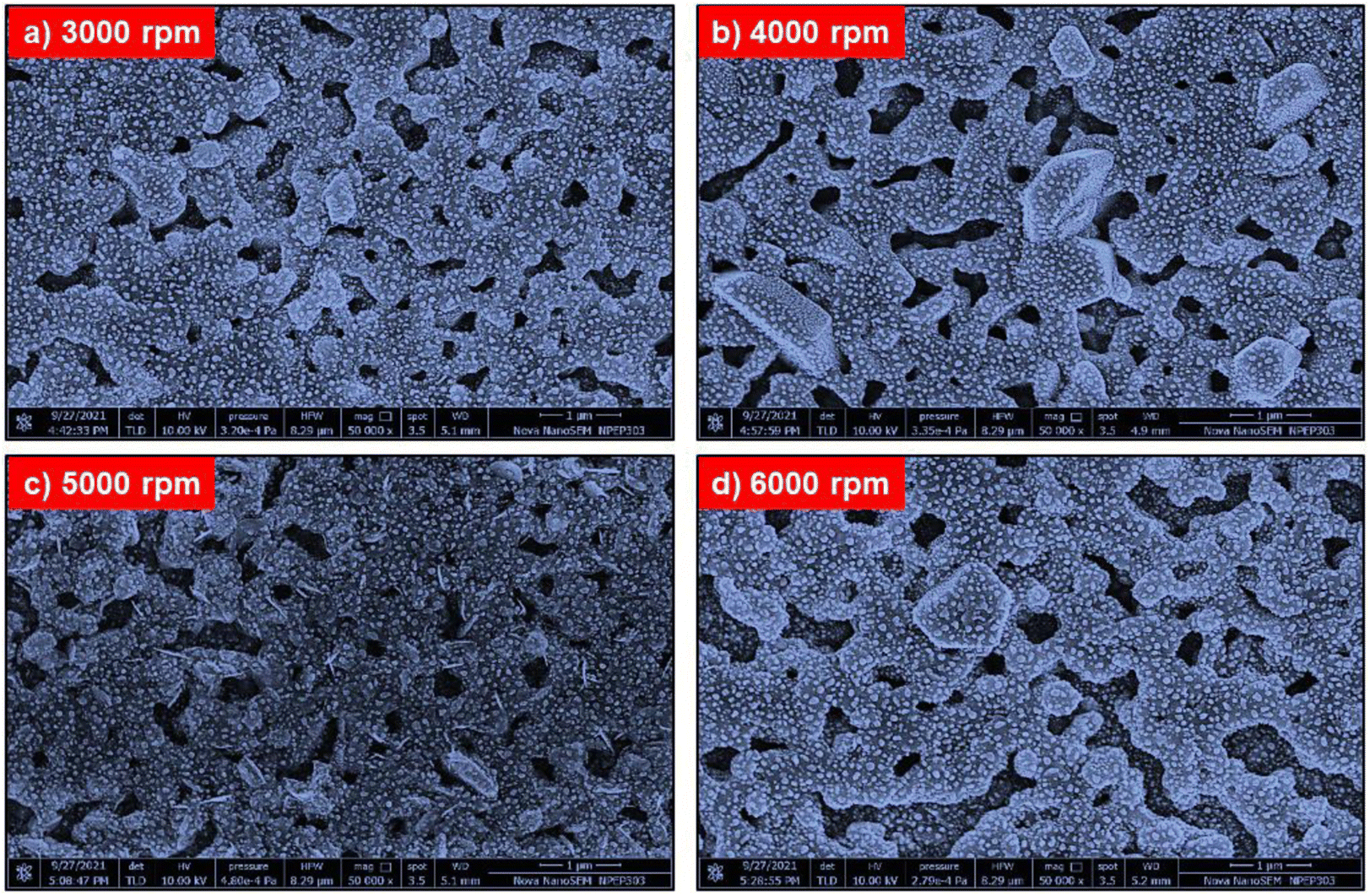
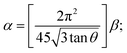
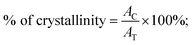
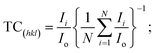
The film's surface morphology and surface chemistry are crucial for improving the device's performance.58 Thus, we investigated the effect of spin speed on the morphological properties, such as surface coverage and grain orientations, of BiI3 thin films. Fig. 5 shows FE-SEM images of BiI3 films deposited at different spin speeds. Before imaging, films were coated with Pt by the sputtering method. The FESEM images for all BiI3 films are homogeneous, dense, and free from flaws, cracks, and protrusions. It was observed that the change in spin speed invokes a distinct difference in grain growth. As a result, the films show an island-like morphology with grain boundaries having different grain sizes. Some micro gaps can also be seen in grains. These gaps are created in the growing films due to uneven evaporation of the solvent. The average size of island-like grains is 400–1200 nm. The evolution of the granular morphology of BiI3 particles can also be seen on these grains. The average particle size is 20–150 nm. The BiI3 film prepared at 4000 rpm indicates that the surface is rough with grain boundaries of 100 nm and larger.
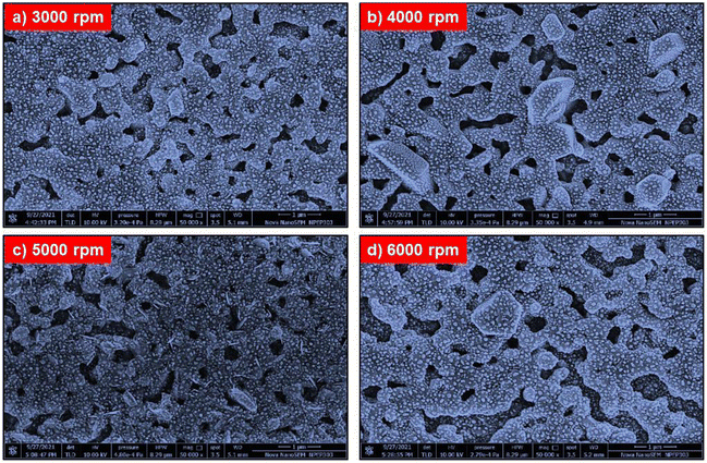 |
| | Fig. 5 FESEM micrographs of BiI3 films prepared at different spin speeds (a) 3000 rpm, (b) 4000 rpm, (c) 5000 rpm, and (d) 6000 rpm. | |
3.4. Optical analysis
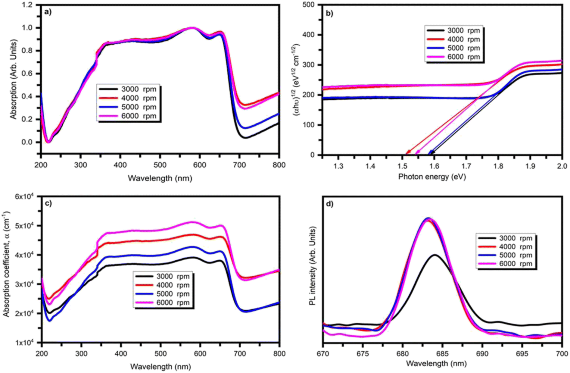
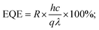
To understand the prominence of BiI3 for optoelectronic applications, optical properties are studied using UV Visible and photoluminescence spectroscopies. Fig. 6(a) shows the absorption profile of BiI3 films deposited at different spin speeds in the 200–800 nm range. For all BiI3 films, the absorption onset is observed at 700 nm. It was observed that an absorption spectrum shows a wide area of absorbance in the region of UV visible from 350 nm to 650 nm. The highest absorbance is observed for the BiI3 film due to the largest average grain size. The XRD pattern supports this conjecture. It was found that the optical bandgaps calculated from different methods are quite different. However, the most reliable method for determining the bandgap of BiI3 is UV-Visible spectroscopy.59 Thus, the optical bandgap (Eg) is evaluated from the absorption coefficient as a part of wavelength. By Tauc's relation, the absorption coefficient (α) and photon energy (hν) are related to each other as,60where α indicates an absorption coefficient, A is the constant, hν indicates photon energy, and n is either 2 or 1/2 for a direct or an indirect bandgap semiconductor. The absorption coefficient (α) is calculated using,61| |
 | (12) |
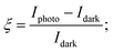
where t represents the thickness of the films. Tauc's plot of prepared BiI3 films at different spin speeds is shown in Fig. 6(b). The calculated band gap values are 1.59, 1.51, 1.54, and 1.58 eV for BiI3 films prepared at 3000, 4000, 5000, and 6000 rpm, respectively, and match with the previously reported values.62 These results indicate that the spin speed does not influence the bandgap of BiI3 films. As seen in Fig. 6(c), BiI3 films prepared at different spin speeds have a much higher absorption coefficient of ∼104 cm−1 in the visible spectra region. The BiI3 film prepared at 4000 rpm has a remarkable absorption coefficient compared to 5000 and 6000 rpm, resulting in the potential candidature for photodetector application as the penetration depth of the radiation into the device material is determined by the absorption coefficient.
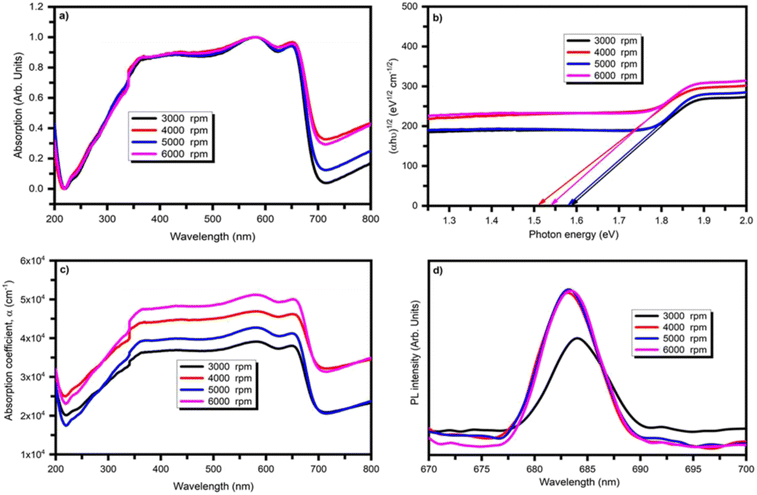 |
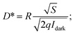
| | Fig. 6 (a) Optical absorption spectra of BiI3 films (b) Tauc's plot used to estimate the bandgap and (c) absorption coefficient (d) photoluminescence spectra of BiI3 films at different rotation speeds. | |
The photoluminescence (PL) study explains the material's bandgap, states of defect, and recombination processes. The PL plots for BiI3 thin films prepared at different spin speeds at a wavelength of 620 nm are shown in Fig. 6(d). No significant shift was observed in the PL peak position for change in spin speed. Instead, the resultant PL peaks were observed at wavelengths ∼683–690 nm, corresponding to 1.82–1.78 eV.
3.5. Photodetector analysis
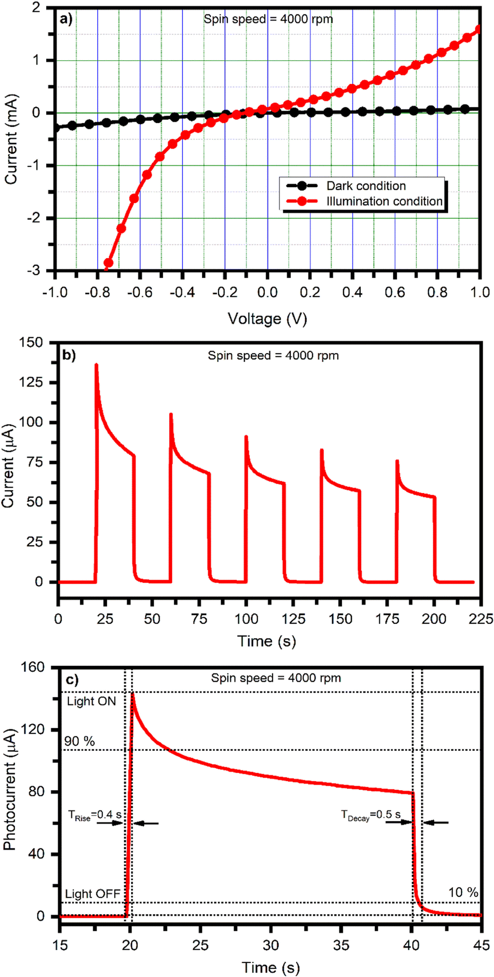
The photodetector working mechanism is based on converting absorbed photons into an electric signal. The basic functioning of the photodetector and various associated mechanisms are well explained in the literature.63–65 As seen from the structural properties, BiI3 films are highly crystalline, and the optical properties show that BiI3 films have optical absorption below 720 nm. Thus, photodetectors were fabricated by depositing BiI3 at different spin speeds (or thicknesses) on an FTO substrate in FTO/c-TiO2/BiI3/graphite configuration. Fig. 7 shows the typical photodetector properties of the BiI3-based photodetector fabricated using thin film prepared at 4000 rpm. Herein, the photoresponse of the BiI3-based system is evaluated under dark and white-light illumination (100 mW cm−2) at room temperature at 0 V (self-bias). Fig. 7(a) shows the current–voltage (I–V) characteristics of the BiI3-based photodetector under both dark and white light illumination conditions. The semiconducting behavior of the prepared BiI3 films is confirmed as the current increases under white light illumination. Fig. 7(b) shows the current versus time (I–t) plot of the fabricated BiI3-based photodetector device at no bias voltage. The device exhibited a constant current over the number of cycles, good repeatability, and stability.
 |
| | Fig. 7 BiI3-based photodetector device characteristics for spin speed 4000 rpm (a) typical current–voltage (I–V) characteristics for dark and under white light illumination, (b) current versus time plot for dark and under white light illumination conditions, and (c) current versus time plot for rise and decay time measurement. | |
The photodetector's rise time (τRise) is the time required to reach 90% of its maximum photocurrent value from its dark current value. Similarly, the photodetector's decay time (τDecay) is the time required to reach 10% of its minimum dark current value from its photocurrent value.66 The photodetector's rise and decay times were calculated by enlarging a single photoresponse cycle. Fig. 7(c) shows a single cycle I–t curve of the BiI3-based photodetector for calculating the rise and decay time for a spin speed of 4000 rpm. The rise and decay time values are ∼0.4 s and ∼0.5 s, respectively. The presence of defects and the recombination of charge carriers strongly affect the response of a photodetector. The surface morphology of the films also affects the carrier transportation and, thus, the device's performance. It has been reported that void and crack-free films are required for ideal optoelectronic devices.67 The fast rise and decay times observed for the BiI3-based photodetector are due to the film's void-free nature and compact surface morphology, enhancing the charge transport of photoinduced charge carriers within the material. XRD (Fig. 4) and FESEM (Fig. 5) analyses further support this conjecture.
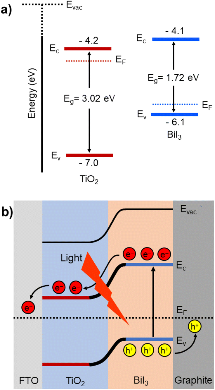
Fig. 8 shows the schematic of the band diagram and photogenerated electron transport mechanism of the BiI3-based photodetector at 0 V bias condition. The energy level positions are obtained from the reported data.68 The rectifying behavior can be attributed to formation of a barrier between the TiO2–BiI3 interface due to difference in energy levels. In the present case, the energy difference between the conduction band maxima of BiI3 and TiO2 is ∼0.1 eV. Therefore, upon illumination, the photogenerated electrons can be pulled quickly towards TiO2 and the external contacts at zero external bias.
 |
| | Fig. 8 (a) Band diagram and (b) photogenerated electron transport mechanism of the BiI3-based photodetector at 0 V bias condition. | |
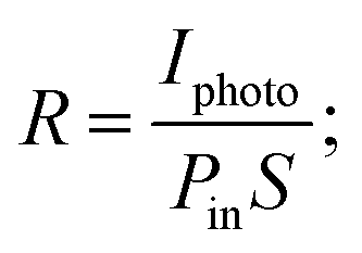
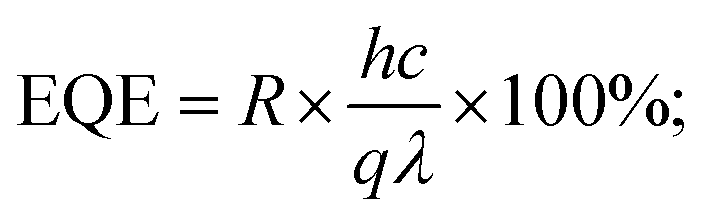
Further, the performance of the BiI3-based photodetector fabricated at 4000 rpm was examined by determining the photosensitivity (ξ), photoresponsivity (R), external quantum efficiency (EQE), and detectivity (D*). The photoresponsivity parameter regulates the briskness of the response to an optical signal of a photodetector. It is represented by the photocurrent produced per unit incidence of light power density on the device,69
| |
 | (13) |
where
Iphoto is the generated photocurrent,
S is the active area of the photodetector, and
Pin is the power of incident radiation or light. The calculated value of photoresponsivity for the BiI
3-based photodetector fabricated at 4000 rpm is listed in
Table 2. High crystallinity and crystallite size are responsible for the smooth transport of photogenerated free electrons, significantly improving photodetectors' overall performance.
70
Table 2 Figure of merit for BiI3-based photodetector fabricated at 4000 rpm under white light illumination
| R (μA W−1) |
ξ |
EQE × 10−4 (%) |
D* × 106 (Jones) |
τRise (s) |
τDecay (s) |
| 100 |
51 |
2.2 |
3.69 |
0.4 |
0.5 |
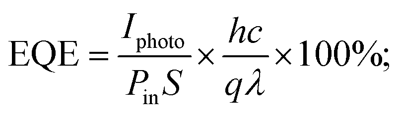
Another critical parameter of a photodetector is its external quantum efficiency (EQE). It gives an idea about the efficiency of photodetectors in converting photons into separated charge carriers.71 It is defined as the ratio of the total number of holes or electrons converted via the stimulation of photons for an applied energy source. It is evaluated by using following equation,72
| |
 | (14) |
where
q is the absolute value of electron charge,
h indicates Planck's constant,
c represents the speed of light, and
λ is the wavelength of illuminated light.
Another crucial parameter of the photodetector is photosensitivity, which represents the change in current with respect to the dark current. The photosensitivity (ξ) is the difference in current (ΔI) normalized to the dark current given by,73
| |
 | (15) |
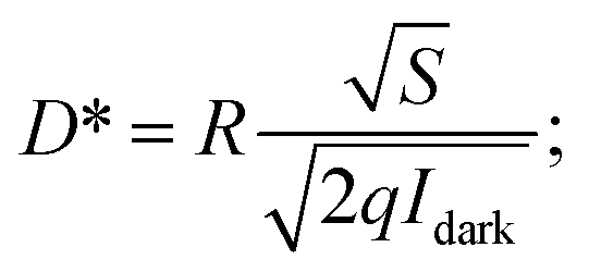
The sensitivity of a device can be recognized by parameter detectivity. It is the ability of a photodetector to sense weak intensity signals. The detectivity of the device is given by74,75
| |
 | (16) |
where
Idark denotes the dark current. The noise limiting detectivity was 10
6 Jones at 0 V bias voltage, comparable to the previously reported detectivity for the BiI
3 photodetector.
The calculated values of photosensitivity (ξ), photoresponsivity (R), external quantum efficiency (EQE), and detectivity (D*), along with the rise time (τRise) and decay time (τDecay) of the BiI3-based photodetector fabricated using thin film prepared at 4000 rpm, are listed in Table 2.
The photosensitivity (ξ), detectivity (D*), rise time (τRise), and decay time (τDecay) of some recently reported BiI3-based photodetectors fabricated using different methods are compared with the present work in Table 3.
Table 3 Comparative analysis of some recently reported BiI3-based photodetectors
| Fabrication method |
ξ |
D* (Jones) |
τRise/τDecay |
Ref. |
| Spin-coating |
0.5 mA W−1 @ 0 V |
1.3 × 10⁷ |
2 s/1 s |
76 |
| PVD |
2.2 A W−1 @ 5 V |
1.6 × 10¹² |
2 s/5.3 ms |
77 |
| PVD |
2.8 A W−1 @ 5 V |
1.2 × 10¹² |
3 s/9 ms |
78 |
| Spin-coating |
100 μA W−1 @ 0 V |
3.9 × 10⁶ |
0.4 s/0.5 s |
Present work |
Although the rise time and decay time observed for our BiI3-based photodetector are 0.4 s and 0.5 s, respectively, the material still has a lot of scope for improvement and needs to be explored further. Nevertheless, after comparing, we found that the photodetector has appreciable performance at 0 V bias (self-biased) than the BiI3-based photodetectors tested at applied biases. Thus, we believe that BiI3 can be a promising material for photodetector application.
4. Conclusions
In conclusion, we have prepared BiI3 thin films via simple and one-step spin coating technique at different spin speeds. The morphological, structural, and optical properties of BiI3 films prepared at 3000–6000 rpm were investigated. The formation of BiI3 films was confirmed through the XRD pattern and revealed that BiI3 has a rhombohedral crystal structure. FESEM analysis showed that BiI3 thin films prepared at different rpm are homogeneous, dense, and free from flaws, cracks, and protrusions. In addition, films show an island-like morphology with grain boundaries having different grain sizes, micro gaps, and the evolution of the granular morphology of BiI3 particles. Furthermore, the UV-Visible and photoluminescence spectroscopy study indicate that the BiI3 films absorb light strongly in the visible spectra region with a higher absorption coefficient (∼104 cm−1) and have an optical band gap of ∼1.51 eV. Finally, a photodetector was fabricated using a BiI3 thin film prepared at an optimum spin speed of 4000 rpm and showed the fast rise and decay times of 0.4 s and 0.5 s, a responsivity of ∼100 μA W−1, the external quantum efficiency of 2.1 × 10⁻⁴%, and a detectivity ∼3.69 × 10⁶ Jones at a 0 V bias. The present results demonstrated that BiI3 could be a promising candidate for other optoelectronic applications.
Author contributions
Ashvini Punde: conceptualization, methodology, investigation and writing-original draft. Shruti Shah: investigation and methodology. Yogesh Hase: visualization and formal analysis. Ashish Waghmare: visualization and formal analysis. Pratibha Shinde: visualization and formal analysis. Bharat Bade: visualization and formal analysis. Habib Pathan: formal analysis and validation. Mohit Prasad: formal analysis and validation. Shashikant Patole: writing-review and editing. Sandesh Jadkar: supervision, writing-review, and editing.
Conflicts of interest
There are no conflicts to declare.
Acknowledgements
Ashvini Punde is grateful to the Mahatma Jyotiba Phule Research and Training Institute (MAHAJYOTI), Government of Maharashtra, for the Mahatma Jyotiba Phule Research Fellowship (MJPRF). Shruti Shah, Yogesh Hase, Ashish Waghmare, Pratibha Shinde, and Bharat Bade are thankful to the Ministry of New and Renewable Energy (MNRE), Government of India, for the financial support under the National Renewable Energy Fellowship (NREF) program. Mohit Prasad and Sandesh Jadkar thank the Indo-French Centre for the Promotion of Advanced Research-CEFIPRA, Department of Science and Technology, New Delhi, for special financial support. Finally, Shashikant P. Patole would like to thank Khalifa University for its financial support through the internal fund for high-quality publications.
References
- X. Gong, M. Tong, Y. Xia, W. Cai, J. S. Moon, Y. Cao, G. Yu, C. L. Shieh, B. Nilsson and A. J. Heeger, Science, 2009, 325, 1665 CrossRef CAS PubMed.
- R. D. Jansen-vanVuuren, A. Armin, A. K. Pandey, P. L. Burn and P. Meredith, Adv. Mater., 2016, 28, 4766 CrossRef CAS PubMed.
- K. J. Baeg, M. Binda, D. Natali, M. Caironi and Y. Y. Noh, Adv. Mater., 2013, 25, 4267 CrossRef CAS PubMed.
- H. Wang and D. H. Kim, Chem. Soc. Rev., 2017, 46, 5204 RSC.
- F. P. García de Arquer, A. Armin, P. Meredith and E. H. Sargent, Nat. Rev. Mater., 2017, 2, 1 Search PubMed.
- Y. Guo, C. Liu, H. Tanaka and E. Nakamura, J. Phys. Chem. Lett., 2015, 6, 535 CrossRef CAS PubMed.
- X. Liu, D. Yu, F. Cao, X. Li, J. Ji, J. Chen, X. Song and H. Zeng, Small, 2017, 13, 1700364 CrossRef PubMed.
- J. Xu, L. Chen, Y. W. Dai, Q. Cao, Q. Q. Sun, S. J. Ding, H. Zhu and D. W. Zhang, Sci. Adv., 2017, 3, e1600246 Search PubMed.
- Q. Zeng and Z. Liu, Adv. Electron. Mater., 2018, 4, 1700335 CrossRef.
- C. Xie, C. Mak, X. Tao and F. Yan, Adv. Funct. Mater., 2017, 27, 1603886 CrossRef.
- W. Zheng, Z. Zhang, R. Lin, K. Xu, J. He and F. Huang, Adv. Electron. Mater., 2016, 2, 1600291 CrossRef.
- Q. Wei, J. Chen, P. Ding, B. Shen, J. Yin, F. Xu, Y. Xia and Z. Liu, ACS Appl. Mater. Interfaces, 2018, 10, 21527 CrossRef CAS PubMed.
- S.-X. Li, X.-L. Xu, Y. Yang, Y.-S. Xu, Y. Xu and H. Xia, ACS Appl. Mater. Interfaces, 2021, 13, 31919–31927 CrossRef CAS PubMed.
- U. Bansode and S. Ogale, J. Appl. Phys., 2017, 121, 133107 CrossRef.
- U. Bansode, A. Rahman and S. Ogale, J. Mater. Chem. C, 2019, 7, 6986–6996 RSC.
- S.-X. Li, Y.-S. Xu, C.-L. Li, Q. Guo, G. Wang, H. Xia, H.-H. Fang, L. Shen and H.-B. Sun, Adv. Mater., 2020, 32, 2001998 CrossRef CAS PubMed.
- C. Perumal Veeramalai, S. Feng, X. Zhang, S. V. N. Pammi, V. Pecunia and C. Li, Photonics Res., 2021, 9, 968–991 CrossRef.
- N. Cates and M. Bernechea, APL Mater., 2018, 6, 084503 CrossRef.
- F. Ma, M. Zhou, Y. Jiao, G. Gao, Y. Gu, A. Bilic, Z. Chen and A. Du, Sci. Rep., 2015, 5, 17558 CrossRef CAS PubMed.
- N. Podraza, W. Qiu, B. Hinojosa, H. Xu, M. Motyka, S. Phillpot, J. Baciak, S. McKinstry and J. Nino, J. Appl. Phys., 2013, 114, 033110 CrossRef.
- M. Du and D. Singh, Phys. Rev. B: Condens. Matter Mater. Phys., 2010, 82, 045203 CrossRef.
- A. Lintereur, W. Qiu, J. Nino and J. Baciak, Nucl. Instrum. Methods Phys. Res., Sect. A, 2011, 652, 166 CrossRef CAS.
- H. Han, M. Hong, S. Gokhale, S. Sinnott, K. Jordan, J. Baciak and J. Nino, J. Phys. Chem. C, 2014, 118, 3244 CrossRef CAS.
- D. Tiwari, D. Alibhai and D. Fermin, ACS Energy Lett., 2018, 3, 1882 CrossRef CAS.
- H. E. Ali and Y. Khairy, Vacuum, 2020, 180, 109640 CrossRef CAS.
- M. Matsumoto, K. Hitomi and T. Shoji, IEEE Trans. Nucl. Sci., 2002, 49, 2526 Search PubMed.
- A. Cuna, A. Noguera, E. Saucedo and L. Fornaro, Cryst. Res. Technol., 2004, 39, 912 CrossRef CAS.
- L. Fornaro, A. Cuña, A. Noguera, M. Pérez and L. Mussio, IEEE Trans. Nucl. Sci., 2004, 51, 2461 CAS.
- M. D. Prasad, L. D. Varma Sangani, S. K. Batabyal and M. Ghanashyam Krishna, CrystEngComm, 2018, 20, 4857 RSC.
- H. Yan, H. Ziyu, G. Xu and S. Xiaohong, Chem. Phys. Lett., 2018, 691, 341 CrossRef CAS.
- D. Nason and L. Keller, J. Cryst. Growth, 1995, 156, 221 CrossRef CAS.
- K. M. Boopathi, S. Raman, R. Mohanraman, F. C. Chou, Y. Y. Chen, C. H. Lee, C.-F. C. Chang and C. W. Chu, Sol. Energy Mater. Sol. Cells, 2014, 121, 35 CrossRef CAS.
- S. Takeyama, K. Watanabe and T. Komatsu, J. Appl. Phys., 1990, 29, 710 CrossRef CAS.
- A. Garg, M. Tomar and V. Gupta, Conf. Pap. Sci., 2014, 3, 370436 Search PubMed.
- B. Y. Xia, P. Yang, Y. Sun, Y. Wu, B. Mayers, B. Gates, Y. Yin, F. Kim and H. Yan, Adv. Mater., 2003, 15, 353 CrossRef.
- J. Zhang, C. Guo, Y. Tian and Q. Liu, Chin. Sci. Bull., 2014, 59, 1787 CrossRef.
- X. Cao, L. Zhi, Y. Jia, Y. Li, K. Zhao, X. Cui, L. Ci, D. Zhuang and J. Wei, ACS Appl. Mater. Interfaces, 2019, 11, 7639 CrossRef CAS PubMed.
- M. D. Tyona, Adv. Mater. Res., 2013, 2, 181 CrossRef.
- F. Ma, PhD thesis, Queensland University of Technology, 2017.
- N. Rathore, A. Kulshreshtha, R. Shukla and D. Sharma, Phys. B, 2021, 600, 412609 CrossRef CAS.
- A. Kulkarni, T. Singh, A. K. Jena, P. Pinpithak, M. Ikegami and T. Miyasaka, ACS Appl. Mater. Interfaces, 2018, 10, 9547 CrossRef CAS PubMed.
- N. F. Coutinho, S. Cucatti, R. B. Merlo, J. Maria, C. S. Filho, N. F. Borrero Villegas, F. Alvarez, A. F. Nogueira and F. C. Marques, Sci. Rep., 2019, 9, 11785 CrossRef PubMed.
- M. G. M. Pandian, D. B. Khadka, Y. Shirai, S. Umedov, M. Yanagida, S. Subashchandran, A. Grigorieva and K. Miyano, J. Mater. Chem., 2020, 8, 12173 Search PubMed.
- B. Cullity and S. Stock, Elements of X-ray Diffraction, Princeton Hall, 3rd edn, 2001 Search PubMed.
- X. X. Sun, Y. L. Li, G. H. Zhong, H. P. Lu and Z. Zeng, Phys. B, 2012, 407, 735 CrossRef CAS.
- Y. Kaifu, J. Lumin., 1988, 42, 61 CrossRef CAS.
- T. Karasawa, T. Kawai, I. Akai and Y. Kaifu, J. Lumin., 1988, 40–41, 431 CrossRef CAS.
- S. Shanmugan, D. Mutharasu and I. Razak, J. Nanomater. Bios., 2014, 9, 1125 Search PubMed.
- B. Karunagaran, R. Kumar, D. Mangalaraj, S. Narayandass and G. Rao, Cryst. Res. Technol., 2002, 37, 1285 CrossRef CAS.
- S. Kite, D. Sathe, S. Patil, P. Bhosale and K. Garadkar, Mater. Res. Express, 2018, 6, 026411 CrossRef.
- M. Balaji, J. Chandrasekarann and M. Raja, Mater. Sci. Semicond. Process., 2016, 43, 104 CrossRef CAS.
- A. Pandey, S. Dalal, S. Dutta and A. Dixit, J. Mater. Sci.: Mater. Electron., 2021, 32, 1341 CrossRef CAS.
- H. Zhao, J. Xie, T. Liang, A. Mao, A. Wang, Y. Chen, D. Ma, V. Paley and A. A. Volinsky, AIP Adv., 2018, 8, 095028 CrossRef.
- B. Yahmadi, N. Kamoun, C. Guasch and R. Bennaceur, Mater. Chem. Phys., 2011, 127, 239 CrossRef CAS.
- Y. Wang, W. Tang and L. Zhang, J. Mater. Sci. Technol., 2015, 31, 175 CrossRef CAS.
- B. Wesley Williamson, F. T. Eickemeyer and H. W. Hillhouse, ACS Omega, 2018, 3, 12713 CrossRef PubMed.
- S. Gupta and K. Munirathnam, Indian J. Pure Appl. Phys., 2014, 52, 44 CAS.
- M. G. M. Pandian, D. B. Khadka, Y. Shirai, S. Umedov, M. Yanagida, S. Subashchandran, A. Grigoriev and K. Miyano, J. Mater. Chem. C, 2020, 8, 12173 RSC.
- N. J. Podraza, W. Qiu, B. B. Hinojosa, H. Xu, M. A. Motyka, S. R. Phillpot, J. E. Baciak, S. T. McKinstry and J. C. Nino, J. Appl. Phys., 2013, 114, 033110 CrossRef.
- J. Tauc and A. Menth, J. Non-Cryst. Solids, 1972, 8–10, 569 CrossRef CAS.
- R. K. Sonker, S. R. Sabhajeet and B. C. Yadav, J. Mater. Sci.: Mater. Electron., 2016, 27, 11726 CrossRef CAS.
- A. J. Lehner, Appl. Phys. Lett., 2015, 107, 131109 CrossRef.
- F. Cao, X. Xu, D. Yu and H. Zeng, Nanophotonics, 2021, 10, 2221 CrossRef CAS.
- R. Wang, J. Wang, S. Tan, Y. Duan, Z. K. Wang and Y. Yang, Trends Chem., 2019, 1, 368 CrossRef CAS.
- F. H. L. Koppens, T. Mueller, P. Avouris, A. C. Ferrari, M. S. Vitiello and M. Polini, Nat. Nanotechnol., 2014, 9, 780 CrossRef CAS PubMed.
- D. Guo, Y. Su, H. Shi, P. Li, N. Zhao, J. Ye, S. Wang, A. Liu, Z. Chen, C. Li and W. Tang, ACS Nano, 2018, 12, 12827 CrossRef CAS PubMed.
- Z. Ou, J. Alloys Compd., 2020, 821, 153344 CrossRef CAS.
- L. C. Lee, T. N. Huq, J. L. MacManus-Driscoll and R. L. Z. Hoye, APL Mater., 2018, 6, 084502 CrossRef.
- S. Lin, Y. Lu, J. Xu, S. Feng and J. Li, Nano Energy, 2017, 40, 122 CrossRef CAS.
- P. S. Shewale and Y. S. Yu, J. Alloys Compd., 2016, 654, 79 CrossRef CAS.
- B. Ezhilmaran, A. Patra, S. Benny, M. R. Sreelakshmi, V. V. Akshay, S. V. Bhat and C. S. Rout, J. Mater. Chem. C, 2021, 9, 6122 RSC.
- N. Huo and G. Konstantatos, Adv. Mater., 2018, 30, 1801164 CrossRef PubMed.
- A. D. Mottram, Y. H. Lin, P. Pattanasattayavong, K. Zhao, A. Amassian and T. D. Anthopoulos, ACS Appl. Mater. Interfaces, 2016, 8, 4894 CrossRef CAS PubMed.
- P. H. Chang, C. S. Li, F. Y. Fu, K. Y. Huang, A. S. Chou and C. I. Wu, Adv. Funct. Mater., 2018, 28, 1800179 CrossRef.
- Y. Wang, R. Fullon, M. Acerce, C. E. Petoukhoff, J. Yang, C. Chen, S. Du, S. K. Lai, S. P. Lau, D. Voiry, D. O'Carroll, G. Gupta, A. D. Mohite, S. Zhang, H. Zhou and M. Chhowalla, Adv. Mater., 2017, 29, 1603995 CrossRef PubMed.
- A. Bhorde, S. Nair, H. Borate, S. Pandharkar, R. Aher, A. Punde, A. Waghmare, P. Shinde, P. Vairale, R. Waykar, V. Doiphode, V. Jadkar, Y. Hase, S. Rondiya, N. Patil, M. Prasad and S. Jadkar, New J. Chem., 2020, 44, 11282 RSC.
- R. Wang, J. Wang, S. Tan, Y. Duan, Z.-K. Wang and Y. Yang, Trends Chem., 2019, 1, 368–379 CrossRef CAS.
- Q. Wei, J. Chen, P. Ding, B. Shen, J. Yin, F. Xu, Y. Xia and Z. Liu, ACS Appl. Mater. Interfaces, 2018, 10, 21527–21533 CrossRef CAS PubMed.
|
| This journal is © The Royal Society of Chemistry 2022 |
Click here to see how this site uses Cookies. View our privacy policy here. 
 Open Access Article
 This Open Access Article is licensed under a Creative Commons Attribution-Non Commercial 3.0 Unported Licence
 a,
Mohit Prasadab,
Shashikant P. Patole
a,
Mohit Prasadab,
Shashikant P. Patole