 Open Access Article
Creative Commons Attribution 3.0 Unported Licence
Iontronic memories based on ionic redox systems: operation protocols
Elalyaa
Mohamed
 a,
Nico
Tchorz
a and
Frank
Marlow
 *ab
*ab
aMPI für Kohlenforschung, Kaiser-Wilhelm-Platz 1, Mülheim an der Ruhr, 45470, Germany. E-mail: marlow@mpi-muelheim.mpg.de
bCenter for Nanointegration Duisburg-Essen (CENIDE), University of Duisburg-Essen, Duisburg, 47057, Germany
First published on 16th March 2023
Abstract
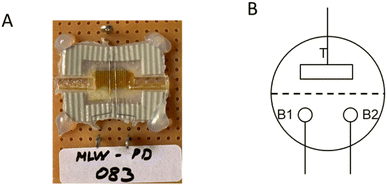
A recently developed, new ionic device called the ionic voltage effect soft triode (IVEST) was optimized, tuned and embedded into a memory application concept. The device is an electrochemical micro-cell, consisting of a top electrode and two bottom electrodes. The device controls the concentration and diffusion of ions via the voltage applied on the top electrode. The device showed a memory effect lasting up to 6 hours. Despite the remarkably large stability time, the memory contrast was small in the first device versions. Now, we have increased the memory contrast by introducing a new external electrical circuit layout combined with a new operation protocol. This new investigation also reveals peculiarities of the memory and shows that the IVEST can be used in memory applications. These iontronic memories show a secondary information storage connected with the read-out frequency.
1 Introduction
Recently, ionic systems have been broadly investigated due to the increased demand for neuromorphic applications, new computing methods, and less energy consumption.1 Different iontronic devices based on the concept of transmitting, generating or storing signals via ions were developed in recent years.2–11 The electric double layer (EDL) formation at the interface between two different materials is considered one of the important processes in iontronics. The EDL at the interface acts as a tiny capacitor with a big capacitance. Beside the capacitance, it has the advantage of combining both the ionic and electronic current in two unalike media. This combination can enable an ionic–electronic transducer and opens the door for a wide range of functionality and applications.12 Another important process in iontronic devices is the diffusion of ions. Ion diffusion results in an exponential concentration gradient that depends on time, making it very interesting in neuromorphic applications as it is reminiscent of short-term plasticity.13,14A switching memory resistor or a memristor is a device with a resistance that depends on the history of the device.15 In resistive switching memory, information is stored in two different states: the high-resistance state (HRS) and the low-resistance state (LRS).16 Different iontronic memristors based on ionic liquids have been reported.17,18 Liquid-electrolyte redox systems can give a promising performance to devices as a result of high-speed faradaic reactions, and a very high pseudocapacitance.19 Such systems may lead to neuromorphic soft materials and a better understanding of the human brain. More investigations on liquid electrolyte redox systems still need to be performed.
In a recent work,20 a new, purely ionic soft triode called an ionic voltage effect soft triode (IVEST) was described. It consists mainly of three electrodes and has amplification and memory characteristics. The basic idea of this device is to control the concentration and diffusion of ions via the voltage applied on the top electrode. The IVEST has two main mechanisms: ion adsorption in a porous electrode and redox oxidizer depletion. It is robust, works reliably, and has several tuning possibilities. The IVEST as an iontronic system differs from electronic systems in working principles and application concepts. In such a system, we cannot measure the same thing two times unless we use well-defined characterization protocols. When, for example, a resistance at a specific point is measured several times it will gradually change. A well-defined protocol is essential to give stable and reproducible results and to obtain high performance from the device. The IVEST has a memory that can last up to 6 h. The drawback of the IVEST memory is the low memory contrast. Therefore, in the present work, we have increased the performance of the device and the memory contrast through technical improvements and introducing new measurement protocols accompanied with a new circuit configuration.
2 Experimental details
2.1 Device construction
Some technical modifications were added to the former construction method.20In some experiments, the TiO2 nanoparticle coating was repeated several times, described by the TiO2 thickness factor Xt.
2.2 Characterization methods
In our previous work, we characterized the IVEST with different configurations.20 Here, we have used a modified configuration with new protocols especially suited for memory operation (see Fig. 2). The layout of the circuit includes a temporary short-cut between the two bottom electrodes controlled by switch S3, a control voltage and a multimeter (IDM93N, RS PRO GmbH) between the two bottom electrodes.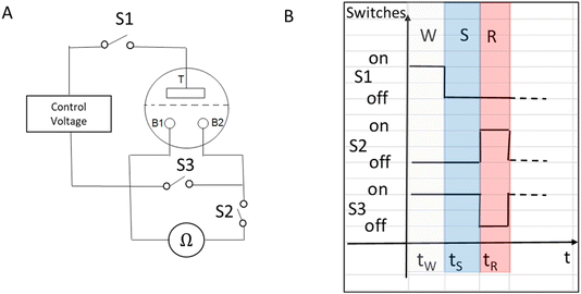 | ||
| Fig. 2 (A) Memory configuration with a temporary short-cut instead of the bypass used before.20 (B) Timeline of the writing–storing–reading (W–S–R) protocol. | ||
Two versions of a special protocol were used to investigate the memory characteristics of the device. Each of these two versions consists of three different phases: writing (W), storing (S) and reading (R). Each phase has a specific time, to give reproducible and controllable results after a series of such processes. The first protocol is called W–S–R and uses cyclic W–S–R phases applied to the IVEST. This protocol is used to measure the basic RBB (resistance between the two bottom electrodes) readouts, dependent on the writing voltages (Vtop) or the voltage applied on the top electrode and a possible hysteresis, as described in Section 3.1. The second protocol is called W–(S–R)n and uses n repeated S–R phases to emulate repeated reading actions, as in natural memories where the readings can be taken several times. It is used to investigate the memory contrast between the high-resistance state (HRS) and the low-resistance state (LRS) as well as their dynamics, as discussed in Section 3.3. Specifically, we have used the times shown in Table 1. To achieve better control during the reading phase, a special electronic switch S2 was added to the circuit. This switch sets the reading time to 1.5 s in this work. We chose the reading time of 1.5 s because it allows reproducible working with a multimeter and restricts the measurement effects of the multimeter. It can be tuned according to needs.
| Protocol | t W/s | t S/s | t R/s |
|---|---|---|---|
| W–R | 10 | 0 | 1.5 |
| W–S–R | 10 | 5 | 1.5 |
| W–(S–R)n | 60 | 20 | 1.5 |
3 Results and discussion
3.1 RBB readout and hysteresis
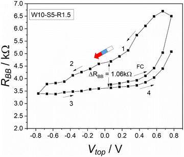
The protocol W–S–R consists of three phases. Each phase has a defined time, as shown in Table 1. These phases also occur in many other memory operation processes. As shown in Fig. 3, we investigated the dependence on the writing voltage. This can be used to find out the range of efficient writing voltages and the conditions for storing information. As we can see in Fig. 3, the device shows a pronounced hysteresis, i.e. the device can be in different states and remember its history. Quantitatively, Fig. 3 shows a hysteresis with a width of ΔRBB = 1.06 kΩ (at Vtop = −0.07 V).However, the interpretation of this result is not completely straight-forward. For sure there is an effect of the top voltage, this being the desired or primary memory effect. In addition, however, one must expect an effect of the read-out process. In detail, when the electrolyte is injected into the device, an electric double layer is created around each electrode.23,24 To measure the resistance, the multimeter injects a current into the system that cause changes in these double layers or their surroundings. In our protocol, the used multimeter injects a charge of 15 μC. Most importantly, the injected charge likely causes a partial depletion of ions at the involved electrodes. As a result, during the next RBB measurement in this measurement cycle, the system is not the same any more. There is a small disturbance and in particular an ionic depletion in the system. The concentration of the ions around each electrode is not symmetric anymore. With each measurement there is an accumulation of such effects (secondary memory) and this affects the main memory process, which we are trying to measure. In protocol W–S–R, the applied short-cut between the two bottom electrodes was introduced to suppress this secondary memory. In comparison with our former work, we conclude that mainly the suppression of the secondary memory made the hysteresis visible and big, as shown in Fig. 3.
In our former work,20 an additional 4 kΩ resistor was used between the two bottom electrodes to ensure symmetry between them. However, this resistor decreased the memory effect significantly. In addition, the measurement protocol was not well-suited to the current study. When the resistor was replaced with the short-cut and a special memory protocol was applied, the memory effect became more visible during the RBB readout measurement.
3.2 Effect of varying the storing time
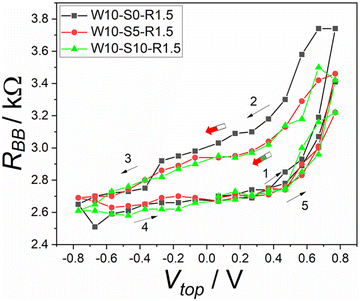
As we mentioned above, each phase of protocol W–S–R has a defined selectable time. In each phase, the system experiences specific processes. In the writing phase a voltage is applied and the state of the system changes. In the storing phase, the system should remain unchanged as much as possible, but if there are changes, resulting gradients will partially equilibrate and possible secondary memory effects will be suppressed. Finally, in the reading phase the resistance between the two bottom electrodes is measured.Fig. 4 shows the effect of varying the storing time. The black curve in Fig. 4 was measured using the protocol W–R (see Table 1) where no storing time was applied after the writing phase. When the storing time was added to the protocol, the hysteresis decreased a little bit (by 0.05 kΩ), as the red and green curves show. The hysteresis width is nearly the same when increasing the storing time from 5 to 10 s, as shown in Fig. 4. This means that the signal can be stored in the device with nearly no dependence on the storing time.
3.3 Effect of the operation modifications on the memory contrast
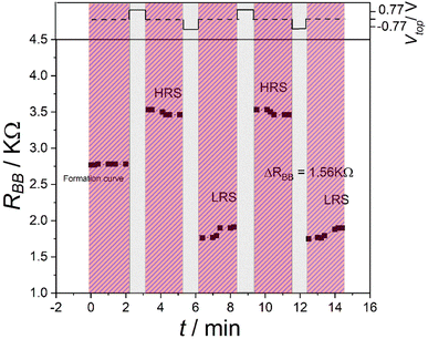
The memory effect can be characterized by the memory contrast, which is the ratio between the high-resistance state (HRS) and the low-resistance state (LRS).In our former investigation, the memory contrast of the device was found to be 1.3 with ΔRBB = 0.56 kΩ,20i.e., the resulting memory contrast was not big. To improve the memory contrast of the device, the new protocol W–(S–R)n was used together with the configuration shown in Fig. 2. For the writing, a positive voltage Vtop = 0.78 was applied on the top electrode for 60 s.
Fig. 5 shows the results of this measurement. Here, a memory contrast α = 1.8, with the difference between the HRS and the LRS ΔRBB = 1.56 kΩ, was reached, which is a significant improvement. The HRS and LRS experienced only small changes, so the memory characteristics were not destroyed at all.
3.4 Device studies
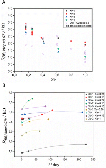
The technical improvements in the construction of the device allowed the control of the fluctuation of the results and increased the stability of the devices, as shown in Fig. 6A and B. As the construction of the IVEST allows many methods of chemical tuning, the performance parameters of different devices vary systematically in a large range of values. The thickness of the titania layer and the electrolyte concentration proved to have a useful tuning effect on the device, as shown in Fig. 6A.Fig. 6A also shows the results for the device constructed with the old construction recipe.20 There is a wide scatter in the resistance measured between the two bottom electrodes. When the new construction method with well-defined geometry and less solvent loss over time was used, the scatter was decreased for each set of devices using the same electrolyte dilution factor and same thickness of TiO2 layer on the top electrode.
The stability of the devices was monitored over days for up to 240 days, as shown in Fig. 6B. The observed changes in the performance are moderate and likely connected with solvent loss. After the technical improvement of the construction method, the devices show better stability.
3.5 Mechanistic aspects
In the IVESTs, different simultaneous processes must be expected with a relative importance dependent on the operation protocol. In general, voltage-induced effects and faradaic processes resulting from the current flow can be expected. The voltage-induced effects were qualitatively discussed in ref. 20. However, for the writing phase in a memory device and the protocols chosen in this work, the current flow is likely of larger importance. During a 1 min-writing phase, 6 mA are typically transported according to Fig. 3A in ref. 20. This induces a local change of 0.03 μmol in the number of triiodide ions. Assuming that this change remains in the vicinity of the electrodes (<0.5 mm), one has to expect concentration changes of 0.9 mM for the top part and 25 mM for the bottom part. As shown in Fig. 7, such changes have actually been observed.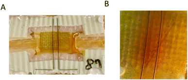 | ||
| Fig. 7 (A) Coloration difference between the two bottom electrodes after applying Vtop = −0.87 V for 1 min. (B) A similar sample under a microscope after applying Vtop = −0.87 V for 1 min. | ||
Here, the triiodide accumulated near to the two bottom electrodes, which is visible in the coloration difference between the two bottom electrodes after applying a Vtop = −0.87 V (Fig. 7). The effects on the top electrode are much less observable because of its bigger size, resulting in lower local concentration changes. In addition, we remark that the depletion of ions will likely have a bigger effect on the conductivity than accumulation. However, depletion of ions is more difficult to observe with the naked eye.
Another aspect of ion transport becomes visible during the readout process. As we have already discussed above, another memory process that we call secondary memory can be explained by the redistribution of the ions between the two bottom electrodes. When a series of resistance measurements is applied between the two bottom electrodes, each readout gives a slightly different value. Each value depends on the history of the number of previous readouts. This secondary memory could be interesting as secondary information storage depending on the readout frequency. In this work, we have concentrated more on the main memory resulting from the non-equilibrium state and the redistribution of the ions between the parts of the device. The secondary memory was suppressed by the chosen operation protocol of applying the short-cut between the two bottom electrodes during the writing phase and the addition of the storing phase. When this secondary memory was suppressed the performance of the device was more stable, reproducible and controllable.
4 Conclusions
In summary, a new operation protocol consisting of writing, storing and reading phases has been reported. A corresponding new external circuit configuration with the addition of a temporal short-cut between the two bottom electrodes has been used. The W–S–R protocol resulted in a pronounced RBB hysteresis. The memory effect was improved and demonstrated using the W–(S–R)n protocol. The memory contrast increased to α = 1.8 with ΔRBB = 1.56 kΩ.The observed processes in the device lead us to the conclusion that the device has more than one memory process. The applied short-cut between the two bottom electrodes managed to suppress the secondary memory to a large extent.
The IVEST memory mechanism is mainly controlled by the redox oxidizer depletion, non-equilibrium states of ion concentrations and the redistribution of the ions between the different electrodes. The suppression of the additional memory allowed the increase of the main memory effect. Based on these results, the IVEST can be used as a memory or a building block for neuromorphic applications. The broad chemical tuning of the device suggests more improvements and possibilities. The construction and the characteristics of the device make it a possibly printable eco-friendly building block for neuromorphic or new computing systems. The avoidance of silicon or other high-purity semiconductors requiring energy-intensive fabrication processes could be essential for this.
Conflicts of interest
The authors declare no conflict of interest.Acknowledgements
The authors would like to thank H. Köster, and U. Petrat for support of the experiments. Open Access funding provided by the Max Planck Society.References
- C. Wan, K. Xiao, A. Angelin, M. Antonietti and X. Chen, Adv. Intell. Syst., 2019, 1, 1900073 CrossRef
.
- J. Odent, N. Baleine, V. Biard, Y. Dobashi, C. Vancaeyzeele, G. T. Nguyen, J. D. Madden, C. Plesse and J. M. Raquez, Adv. Funct. Mater., 2022, 2210485 Search PubMed
.
- E. O. Gabrielsson, K. Tybrandt and M. Berggren, Lab Chip, 2012, 12, 2507–2513 RSC
.
- S.-M. Lim, H. Yoo, M.-A. Oh, S. H. Han, H.-R. Lee, T. D. Chung, Y.-C. Joo and J.-Y. Sun, Proc. Natl. Acad. Sci. U. S. A, 2019, 116, 13807–13815 CrossRef CAS PubMed
.
- P. Janson, E. O. Gabrielsson, K. J. Lee, M. Berggren and D. T. Simon, Adv. Mater. Technol., 2019, 4, 1800494–1800500 CrossRef
.
- Z. Q. Wang, H. Y. Xu, X. H. Li, H. Yu, Y. C. Liu and X. J. Zhu, Adv. Funct. Mater., 2012, 22, 2759–2765 CrossRef CAS
.
- K. Tybrandt, R. Forchheimer and M. Berggren, Nat. Commun., 2012, 3, 871 CrossRef PubMed
.
- A. Williamson, J. Rivnay, L. Kergoat, A. Jonsson, S. Inal, I. Uguz, M. Ferro, A. Ivanov, T. A. Sjöström, D. T. Simon, M. Berggren, G. G. Malliaras and C. Bernard, Adv. Mater., 2015, 27, 3138–3144 CrossRef CAS PubMed
.
- K. Tybrandt, E. O. Gabrielsson and M. Berggren, J. Am. Chem. Soc., 2011, 133, 10141–10145 CrossRef CAS PubMed
.
- R. Li, Y. Si, Z. Zhu, Y. Guo, Y. Zhang, N. Pan, G. Sun and T. Pan, Adv. Mater., 2017, 29, 1700253 CrossRef PubMed
.
- P. Robin, T. Emmerich, A. Ismail, A. Niguès, Y. You, G.-H. Nam, A. Keerthi, A. Siria, A. Geim and B. Radha, Science, 2023, 379, 161–167 CrossRef CAS PubMed
.
- I. Gorelov, S. Ryasenskii, S. Kartamyshev and M. Fedorova, J. Anal. Chem., 2005, 60, 65–69 CrossRef CAS
.
- J. Y. Gerasimov, R. Gabrielsson, R. Forchheimer, E. Stavrinidou, D. T. Simon, M. Berggren and S. Fabiano, Adv. Sci., 2019, 6, 1801339 CrossRef PubMed
.
- Y. H. Liu, L. Q. Zhu, P. Feng, Y. Shi and Q. Wan, Adv. Mater., 2015, 27, 5599–5604 CrossRef CAS PubMed
.
- R. Waser, R. Dittmann, G. Staikov and K. Szot, Adv. Mater., 2009, 21, 2632–2663 CrossRef CAS PubMed
.
- L. Gao, Q. Ren, J. Sun, S.-T. Han and Y. Zhou, J. Mater. Chem. C, 2021, 9, 16859–16884 RSC
.
- P. Zhang, M. Xia, F. Zhuge, Y. Zhou, Z. Wang, B. Dong, Y. Fu, K. Yang, Y. Li and Y. He, Nano Lett., 2019, 19, 4279–4286 CrossRef CAS PubMed
.
- B. Sun, S. Ranjan, G. Zhou, T. Guo, C. Du, L. Wei, Y. N. Zhou and Y. A. Wu, ACS Appl. Electron. Mater, 2021, 3, 2380–2388 CrossRef CAS
.
- E. Frackowiak, M. Meller, J. Menzel, D. Gastol and K. Fic, Faraday Discuss., 2014, 172, 179–198 RSC
.
- E. Mohamed, S. Josten and F. Marlow, Phys. Chem. Chem. Phys., 2022, 24, 8311–8320 RSC
.
- S. Josten, T. Koehler and F. Marlow, Solar Energy, 2022, 247, 346–354 CrossRef CAS
.
- P. R. F. Barnes, K. Miettunen, X. Li, A. Y. Anderson, T. Bessho, M. Grätzel and B. C. O'Regan, Adv. Mater., 2013, 25, 1881–1922 CrossRef CAS PubMed
.
-
S. Srinivasan, Fuel Cells: From Fundamentals to Applications, Springer Science & Business media, 2006 Search PubMed
.
-
A. J. Bard and L. R. Faulkner, Electrochemical Methods: Fundamentals and Applications, Wiley, New York, 1980 Search PubMed
.
| This journal is © The Royal Society of Chemistry 2023 |

