 Open Access Article
Efficient furan-bridged dibenzofulvene-triphenylamine hole transporting materials for perovskite solar cells†
Nan
Wu‡
a,
Xianfu
Zhang‡
a,
Xuepeng
Liu
 *a,
Ying
Wang
a,
Mingyuan
Han
a,
Rahim
Ghadari
b,
Yahan
Wu
*c,
Yong
Ding
 a,
Molang
Cai
 a and
Songyuan
Dai
 *a
*a
aBeijing Key Laboratory of Novel Thin-Film Solar Cells, North China Electric Power University, Beijing 102206, China. E-mail: liuxuepeng@ncepu.edu.cn; sydai@ncepu.edu.cn
bComputational Chemistry Laboratory, Department of Organic and Biochemistry, Faculty of Chemistry, University of Tabriz, Tabriz 51666164, Iran
cCollege of Energy and Power Engineering, Inner Mongolia University of Technology, Huhhot, 010051, P. R. China. E-mail: 460253698@qq.com
First published on 7th December 2022
Abstract
Inspired by the superior properties of dibenzofulvene-triphenylamine hole transporting materials (HTMs), a rationally designed type of HTM with furan as the side-arm bridge has been synthesized, namely, FF-OMeTPA. A dibenzofulvene-triphenylamine HTM with thiophene as the side-arm bridge (FT-OMeTPA) is also prepared. The effect of heteroatomic sulfur-to-oxygen change on the molecular and photovoltaic properties in perovskite solar cells was investigated. The experimental and theoretical results illustrate that the furan-based molecule has better conjugation than the thiophene-based one, leading to higher hole mobility. The PSC employing oxygen-containing FF-OMeTPA delivered a power conversion efficiency (PCE) of 21.82%, whereas the FT-OMeTPA-based PSC exhibited a lower PCE of 18.01%. Significantly, the FF-OMeTPA-based devices also outperform those employing conventional spiro-OMeTAD. In addition, the studied molecules exhibit comparable device stability and much lower synthesis cost than spiro-OMeTAD.
Introduction
Perovskite solar cells (PSCs) have drawn wide attention because of their high efficiency and low-cost preparation process, showing excellent development potential. During recent years, the power conversion efficiency (PCE) of the PSC has rapidly increased from 3.8% to 25.7%.1–6 PSCs have a sandwich-like structure in which the perovskite layer is sandwiched between the hole transport layer and the electron transport layer. Hole transporting materials (HTMs) play an important role in extracting holes from the absorption perovskite layer and transmitting them to the electrode.7 At the same time, the HTM is conducive to the separation of carriers in the perovskite layer and reduces the influence of carrier recombination on the efficiency and stability of the devices.8,9 At present, the reported HTMs can be roughly divided into three categories: inorganic semiconductors, polymers, and organic small-molecular HTMs. Of these, small-molecular HTMs have attracted much attention because of the minor differences among different batches, the easy solution preparation process, and the fact that their molecular properties can be optimized by cutting and tuning the molecular structure.10,11 To date, small-molecular 2,2′,7,7′-tetrakis(N,N-di-p-methoxyphenyl)-amine-9,9′-spirobifluorene (spiro-OMeTAD) is a commonly used HTM, and devices using this material have the highest PCE of PSCs.4,12 However, the complex preparation process and inferior hole mobility of spiro-OMeTAD led to the development of a lot of new alternatives with varied building blocks.13 Among the reported small-molecular HTMs, dibenzofulvene-triphenylamine molecules with thiophene as the side-arm bridge have been widely used for efficient p–i–n PSCs.14–17 On the other hand, the introduction of heteroatomic oxygen or sulfur into the molecular structure has been widely used to tune the properties of small organic molecule HTMs in PSCs.18–20 There are lone electron pairs on oxygen-containing or sulfur-containing functional groups such as thiophene and furan, which can interact with perovskites, provide exchange channels between holes and perovskites, and passivate perovskite surface defects;21,22 in addition, the interaction between heteroatoms can also promote molecular packing and improve hole mobility.23 In our previous reports, we noted that the HTMs with an oxygen-containing furan unit or similar structures exhibit higher device PCEs than those with a sulfur-containing thiophene unit.24–26 Inspired by these results, a new dibenzofulvene-triphenylamine HTM with furan as the side-arm bridge (FF-OMeTPA) has been designed and prepared. The introduction of heteroatom oxygen and sulfur can adjust the energy level and improve the morphology of the film. Therefore, a dibenzofulvene-triphenylamine HTM with thiophene as the side-arm bridge (FT-OMeTPA) is also selected as the reference, which has been proved as an efficient HTM for p–i–n PSCs.15The chemical structures of FT-OMeTPA and FF-OMeTPA are shown in Fig. 1a. Both FT-OMeTPA and FF-OMeTPA exhibit suitable band energy alignment with perovskite and similar thermal stability. Interestingly, the hole mobility of the molecule is enhanced by altering thiophene with furan, resulting in a better hole migration ability. When used in PSCs, the furan-containing FF-OMeTPA-based device displays a high PCE of 21.82%, which is substantially higher than the devices with FT-OMeTPA (PCE = 18.01%) and conventional spiro-OMeTAD (PCE = 21.02%).
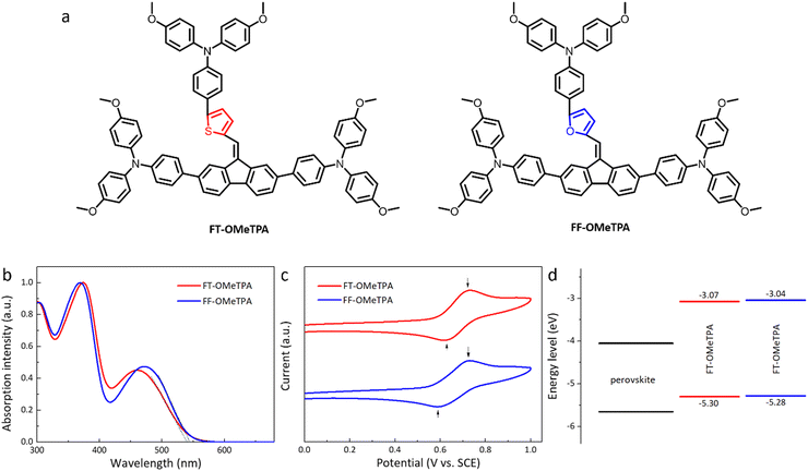 | ||
| Fig. 1 (a) Chemical structure of FT-OMeTPA and FF-OMeTPA. (b) Normalized UV-Vis absorption spectra in DCM solution. (c) CV of FT-OMeTPA and FF-OMeTPA. (d) Molecular energy level alignments. | ||
Results and discussion
The effect of heteroatomic sulfur-to-oxygen change on the optical properties is studied by ultraviolet-visible (UV-Vis) absorption measurements. The normalized UV-Vis spectra of FT-OMeTPA and FF-OMeTPA in DCM solution are shown in Fig. 1b. The related data are listed in Table 1. The absorption peak wavelengths of FT-OMeTPA are 375 nm and 460 nm, respectively; the absorption peak wavelengths of FF-OMeTPA are 369 nm and 472 nm, respectively. The absorption peak near 300 nm wavelength is mainly due to the existence of a benzene ring and C![[double bond, length as m-dash]](https://www.rsc.org/images/entities/char_e001.gif) C, which causes the π–π* transition to overlap with the vibration of the benzene ring.19 The most substantial absorption peaks in the wavelength range of 300–400 nm were mainly attributed to the n–π* transition of unbonded lone electrons on thiophene/furan. In addition, the absorption peaks of FT-OMeTPA and FF-OMeTPA in the visible regions are caused by the intramolecular charge transfer transition (ICT) between donor and acceptor units, illustrating better π conjugation through FF-OMeTPA.19,27,28 Besides, Fig. S1 (ESI†) illustrates the absorption spectra of FT-OMeTPA and FF-OMeTPA in the film state. The absorption edge is significantly red-shifted from solution to film (15 nm and 14 nm for FT-OMeTPA and FF-OMeTPA, respectively), which has been noted in many conjugated materials.29,30 The optical bandgap (Eg) of FT-OMeTPA and FF-OMeTPA is calculated to be 2.23 eV and 2.24 eV (from the absorption spectra of the film state), respectively.
C, which causes the π–π* transition to overlap with the vibration of the benzene ring.19 The most substantial absorption peaks in the wavelength range of 300–400 nm were mainly attributed to the n–π* transition of unbonded lone electrons on thiophene/furan. In addition, the absorption peaks of FT-OMeTPA and FF-OMeTPA in the visible regions are caused by the intramolecular charge transfer transition (ICT) between donor and acceptor units, illustrating better π conjugation through FF-OMeTPA.19,27,28 Besides, Fig. S1 (ESI†) illustrates the absorption spectra of FT-OMeTPA and FF-OMeTPA in the film state. The absorption edge is significantly red-shifted from solution to film (15 nm and 14 nm for FT-OMeTPA and FF-OMeTPA, respectively), which has been noted in many conjugated materials.29,30 The optical bandgap (Eg) of FT-OMeTPA and FF-OMeTPA is calculated to be 2.23 eV and 2.24 eV (from the absorption spectra of the film state), respectively.
| HTM | λ abs (nm) | E g (eV) | HOMOc (eV) | LUMOd (eV) | T g (°C) | μ (cm2 V−1 s−1) | σ (S cm−2) |
|---|---|---|---|---|---|---|---|
| a The absorption peak in DCM solution. b Determined from the UV-Vis absorption edge (film state, Fig. S1, ESI). c Measured in tetra-n-butyl ammonium hexafluorophosphate solution, using three electrode systems with Fc/Fc+ as an external standard. d Calculated from ELUMO = EHOMO + Eg. | |||||||
| FT-OMeTPA | 375, 460 | 2.23 | −5.30 | −3.07 | 106 | 2.72 × 10⁻⁴ | 2.68 × 10⁻⁴ |
| FF-OMeTPA | 369, 472 | 2.24 | −5.28 | −3.04 | 115 | 4.34 × 10⁻⁴ | 3.67 × 10⁻⁴ |
The highest occupied molecular orbital (HOMO) level of the molecules is determined by cyclic voltammetry (CV), as shown in Fig. 1c. With ferrocene/ferrocenium (Fc/Fc+) as the reference, the HOMO energy levels of FT-OMeTPA and FF-OMeTPA are around −5.30 eV and −5.28 eV, respectively, which can well match the valence band of the perovskite (∼−5.65 eV) and is conducive to the migration of holes to the electrode. The lowest unoccupied molecular orbital (LUMO) levels of FT-OMeTPA and FF-OMeTPA are calculated to be −3.00 eV through HOMO and Eg. The significantly higher LUMO level of them compared with that of the perovskite conduction band (∼−4.05 eV) ensures an effective blocking of electron transport to the electrodes. The molecular energy level alignments with perovskite are shown in Fig. 1d.
To further understand the electron density distribution, electrostatic surface potential diagram, and optimized geometric structure of frontier molecular orbitals of FT-OMeTPA and FF-OMeTPA, time-dependent density functional theory (DTDFT) calculations are performed at the B3LYP/6-311G* level. As illustrated in Fig. S2 (ESI†), the theoretical calculated HOMO level of FT-OMeTPA and FF-OMeTPA is −4.91 eV and −4.90 eV, which are consistent with the trend of the experimental data. The higher HOMO level of FF-OMeTPA than FT-OMeTPA further illustrates the better conjugation of FF-OMeTPA.31 The electronic density distributions of FT-OMeTPA and FF-OMeTPA are similar. LUMOs are mainly located at the core of fluorene-bridged-thiophene or fluorene-bridged-furan, while HOMOs are located at fluorene and extended methoxytriphenylamine units. Since there are many orbital overlaps in HOMOs of adjacent molecules during molecular accumulation, the HOMO distribution characteristics of these materials are conducive to hole transport.32 At the same time, the distribution characteristics of electronic density in the ground state and excited state of molecules indicate that there is intramolecular charge transfer (ICT) between methoxytriphenylamine and the core, which is also demonstrated by the UV-vis results.33 In the optimized geometry structures (Fig. 2a, top view), the dihedral angle between the fluorene and adjacent thiophene is larger than that of the furan counterpart; therefore, the better planar configuration of FF-OMeTPA (further confirmed by Fig. 2b, side view) may be attributed to the tight molecular packing, which is beneficial to obtain a higher hole mobility.34–37 For the electrostatic surface potential (ESP) of FT-OMeTPA and FF-OMeTPA, the negative electrostatic (red part) and positive electrostatic potential (blue part) are located on the whole molecule and overlap. It is worth noting that compared with the sulfur-containing FT-OMeTPA, the core part of the oxygen-containing FF-OMeTPA has more negative charges, which will give FF-OMeTPA a stronger electron absorption ability.38 The thermal stability of FT-OMeTPA and FF-OMeTPA is evaluated by differential scanning calorimetry (DSC, Fig. S3, ESI†). The glass transition temperatures (Tg) of FT-OMeTPA and FF-OMeTPA are 106 and 115 °C, respectively, which exhibit a similar varied trend to our previous report.24,25 The higher Tg indicates a more amorphous nature, which is beneficial for forming uniform films and enhancing the device stability.29,39
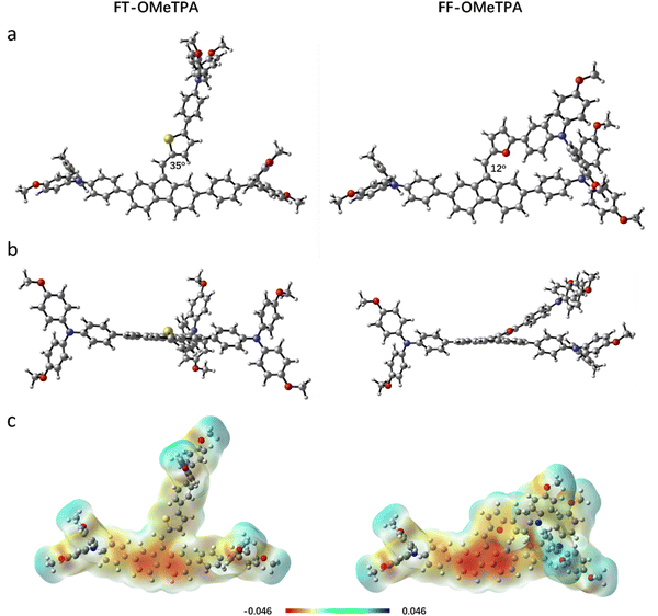 | ||
| Fig. 2 Geometry-optimized configurations of (a) top view and (b) side view. (c) Electrostatic surface potential maps from TDDFT calculations. | ||
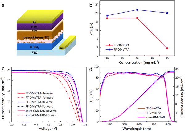
After interpreting the properties of the materials, the conventional n–i–p mesoscopic architecture PSCs with the structure of FTO/bl-TiO2/mp-TiO2/Cs0.05(FA0.85MA0.15)0.95Pb(I0.85Br0.15)3/HTM/Au were fabricated to evaluate the performance of FT-OMeTPA and FF-OMeTPA in solar cells. In the same batch, spiro-OMeTAD as the HTM was also made into the same type of device as a reference. The structure of PSCs is presented in Fig. 3a. The detailed device fabrication process is shown in the ESI.† Previous studies have found that the appropriate deposition amount of HTM has a significant influence on the PCE of PSCs,40–42 and FT-OMeTPA also exhibited this behavior in previous work.15 Therefore, the deposition amount of the investigated HTM on device performance was also explored, and the concentration was 60, 40, and 20 mg mL−1, respectively. As illustrated in Fig. 3b and Table S1 (ESI†), the concentration of HTMs has a noticeable effect on the device performance. When FT-OMeTPA and FF-OMeTPA are at medium concentrations (40 mg mL−1), the PCE of the device is the highest. It is worth noting that the thiophene-containing molecule FT-OMeTPA exhibits a very poor PCE when the concentration is high (60 mg mL−1), but the device exhibits considerable PCE when the concentration decreases. No matter in which concentration, the PCE of FF-OMeTPA in PSCs is higher than that of FT-OMeTPA. Fig. S4 (ESI†) shows a scanning electron microscopy (SEM) image of a device employing the HTM with the concentration of 40 mg mL−1. The device consisted of a TiO2 layer (∼110 nm, including compact and mesoporous layer), perovskite layer (500–600 nm), and a ∼70 nm-thick layer of HTM.
Fig. 3c shows the current density–voltage (J–V) curves of the best-performing PSCs with different HTMs among 16 devices (Table S2, ESI†). The champion FF-OMeTPA-based PSC exhibited a high PCE of 21.82%, with an open-circuit voltage (Voc) of 1.15 V, a short-circuit current density (Jsc) of 24.87 mA cm−2, and a fill factor (FF) of 76%. The PCE of the best FT-OMeTPA-based PSCs was only 18.01%, with a Jsc of 24.08 mA cm−2, a Voc of 1.11 V and an FF of 67%. As a reference, the spiro-OMeTAD-based device exhibits a PCE of 21.02%. Though the device with different HTMs display hysteresis (Fig. 3c), the FF-OMeTPA-based cell exhibits a higher PCE than that of FT-OMeTPA and spiro-OMeTAD. Fig. 3d exhibits the external quantum efficiency (EQE) spectra for the PSCs. It is estimated that the integrated Jsc values of FT-OMeTPA, FF-OMeTPA, and spiro-OMeTAD are 22.51, 23.08, and 22.61 mA cm−2, respectively, which is consistent with the Jsc results of J–V (Table 2).
| HTM | Scan direction | J sc (mA cm−2) | V oc (V) | FF (%) | PCE (%) |
|---|---|---|---|---|---|
| FT-OMeTPA | Reverse | 24.08 | 1.11 | 67 | 18.01 |
| Forward | 24.04 | 1.09 | 60 | 15.78 | |
| FF-OMeTPA | Reverse | 24.87 | 1.15 | 76 | 21.82 |
| Forward | 24.84 | 1.12 | 71 | 19.73 | |
| Spiro-OMeTAD | Reverse | 24.21 | 1.16 | 75 | 21.02 |
| Forward | 24.10 | 1.15 | 69 | 19.14 |
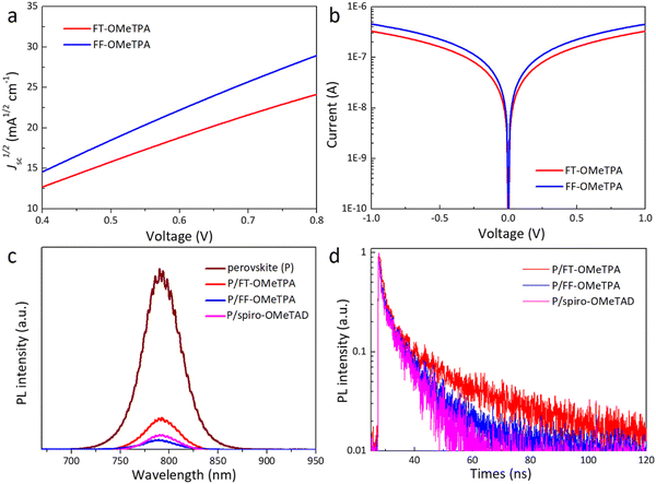
To explore the superior device performance of FF-OMeTPA and the effect of molecular structure on the photovoltaic properties, the carrier mobility, film-forming properties, and hole extraction ability, etc., of different HTMs were investigated. The dark J–V characteristic curve of the hole-only device with a FTO/PEDOT:PSS/perovskite/HTM/Au structure was tested by the space charge-limited current (SCLC) method to study their carrier transport characteristics. The obtained J–V curves and data are shown in Fig. 4a and Table 1. The calculated hole mobility of the oxygen-containing molecule FF-OMeTPA (4.34 × 10⁻⁴ cm2 V−1 s−1) is higher than the sulfur-containing molecule FT-OMeTPA (2.72 × 10⁻⁴ cm2 V−1 s−1). In addition, we fabricated the hole-only devices with a FTO/HTM/Au structure to measure the conductivity of FT-OMeTPA and FF-OMeTPA with additives (Fig. 4b). The result indicates that FF-OMeTPA has the highest conductivity of 3.67 × 10⁻⁴ S cm−2, while FT-OMeTPA has a conductivity of 2.68 × 10⁻⁴ S cm−1. Therefore, the molecule with a furan unit exhibits a higher carrier mobility than that of its thiophene counterpart, which is consistent with the above DFT results (better planar configuration of FF-OMeTPA) and many reported theoretical and experimental results.24,34,35 The series resistance of the FT-OMeTPA-based device will increase more than that of FF-OMeTPA when the HTM layer is thickened, which is the reason why FT-OMeTPA presents a low device performance under a high concentration due to its low carrier mobility.43 On the other hand, the concentration of FF-OMeTPA exhibits a tiny influence on device performance due to its higher carrier mobility.
To evaluate the charge transfer kinetics at the perovskite/HTM interface, steady-state photoluminescence (PL) and time-resolved PL (TRPL) decay measurements were performed. As illustrated in Fig. 4c, compared with the PL spectrum of pure perovskite films grown on glass, the intensity of the steady-state PL spectra is significantly suppressed after HTM deposition on perovskite films, and the order of the suppression effect was FF-OMeTPA > FT-OMeTPA, which was consistent with the trend of hole mobility. Fig. 4d shows the corresponding TRPL curves of the perovskite film with different HTMs. The average decay time (dual-exponential fitting) of FT-OMeTPA, FF-OMeTPA, and spiro-OMeTAD is around 10.0, 5.8, and 5.5 ns, respectively. Therefore, FF-OMeTPA has a relatively strong hole extraction ability compared with FT-OMeTPA,44–46 which could be a factor for the higher device efficiency and Voc.47 Moreover, the hole extraction ability of FF-OMeTPA is also comparable with spiro-OMeTAD.
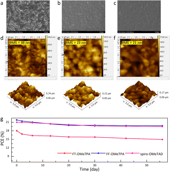
The surface morphology of the HTM films was investigated using scanning electron microscopy (SEM) and atomic force microscopy (AFM). The SEM results (Fig. 5a–c) illustrate that both FT-OMeTPA and FF-OMeTPA could form uniform morphology on the perovskite layer, which could be a result of the superior film morphology of branched HTMs.48,49 The root-mean-square (RMS) roughness value of the perovskite layer is about 49 nm. After the perovskite was coated with HTMs, the RMS values of the FT-OMeTPA and FF-OMeTPA-based films were 23 and 21 nm, respectively. Therefore, FF-OMeTPA would form a slightly more uniform film on the perovskite layer than FT-OMeTPA, which can be a result of its good molecular accumulation.50,51 The surface hydrophobicity of the molecules doped on perovskite is determined by water contact angle measurement (Fig. S5, ESI†). It can be found that the water contact angle decreases after the HTMs were doped, which could be a result of the hydrophilicity of the dopants. Nevertheless, the water contact angle increases after doping a HTM coating on the perovskite surface, which indicates that the HTM can hinder water erosion and improve the stability of the device. Fig. 5b shows the PCE changes of the device in 56 days in a dark environment without encapsulation. The devices are stored at room temperature (∼30 °C) and low humidity (∼10%). It can be seen that the PCEs of all the devices exhibit a slight downward trend, which could be a result of the existence of dopants.21 Nevertheless, the FF-OMeTPA-based device presents relatively better stability than FT-OMeTPA, which should be due to its better thermal stability and hydrophobicity. Finally, the cost of FF-OMeTPA in laboratory synthesis and purification is around 34.5 $ per g (Tables S3 and S4, ESI†), which is remarkably lower than that of spiro-OMeTAD, suggesting its superior application potential.
Conclusion
In summary, a fluorene-bridged-furan triphenylamine-based hole transporting material was designed and developed. Compared with the sulfur-containing thiophene counterpart, the developed furan-based molecule has a higher hole mobility, higher Tg, and smoother surface morphology. When used in PSCs, the furan-based HTM displays a higher PCE with minor hysteresis compared with the thiophene-based one. Notably, the device with a furan-based molecule also surpasses conventional spiro-OMeTAD.Conflicts of interest
There are no conflicts to declare.Acknowledgements
This work was supported by the National Key R&D Program of China (2019YFB1503200), the National Natural Science Foundation of China (61904053), the 111 Project (B16016), the Inner Mongolia Natural Science Foundation (2022QN05013), the Science Foundation of Inner Mongolia University of Technology (BS2021069, ZY202017), the 2020 Inner Mongolia Autonomous Region level talent introduction policy project (DC2100001429), and the basic scientific research business expense project of colleges and universities directly under the Inner Mongolia Autonomous Region (JY20220176).References
- A. Kojima, K. Teshima, Y. Shirai and T. Miyasaka, J. Am. Chem. Soc., 2009, 131, 6050–6051 CrossRef CAS PubMed.
- Q. Jiang, Y. Zhao, X. Zhang, X. Yang, Y. Chen, Z. Chu, Q. Ye, X. Li, Z. Yin and J. You, Nat. Photonics, 2019, 13, 460–466 CrossRef CAS.
- H. Min, M. Kim, S. U. Lee, H. Kim and I. S. Sang, Science, 2019, 366, 749–753 CrossRef CAS PubMed.
- H. Min, D. Y. Lee, J. Kim, G. Kim, K. S. Lee, J. Kim, M. J. Paik, Y. K. Kim, K. S. Kim, M. G. Kim, T. J. Shin and S. I. Seok, Nature, 2021, 598, 444–450 CrossRef CAS PubMed.
- Y. Zhao, F. Ma, Z. Qu, S. Yu, T. Shen, H.-X. Deng, X. Chu, X. Peng, Y. Yuan, X. Zhang and J. You, Science, 2022, 377, 531–534 CrossRef CAS PubMed.
- NREL Best Research-Cell Efficiencies; National Renewable Energy Laboratory, https://www.nrel.gov/pv/assets/pdfs/best-research-cell-efficiencies-rev220126.pdf.
- M. Jeong, I. W. Choi, E. M. Go, Y. Cho, M. Kim, B. Lee, S. Jeong, Y. Jo, H. W. Choi, J. Lee, J.-H. Bae, S. K. Kwak, D. S. Kim and C. Yang, Science, 2020, 369, 1615–1620 CrossRef CAS PubMed.
- Z. H. Bakr, Q. Wali, A. Fakharuddin, L. Schmidt-Mende, T. M. Brown and R. J. Jose, Nano Energy, 2017, 34, 271–305 CrossRef CAS.
- S. S. Reddy, K. Gunasekar, J. H. Heo, S. H. Im, C. S. Kim, D. H. Kim, J. H. Moon, J. Y. Lee, M. Song and S. H. Jin, Adv. Mater., 2016, 28, 686–693 CrossRef CAS PubMed.
- A. Farokhi, H. Shahroosvand, G. Delle Monache, M. Pilkington and M. K. Nazeeruddin, Chem. Soc. Rev., 2022, 51, 5974–6064 RSC.
- P. Murugan, T. Hu, X. Hu and Y. Chen, J. Mater. Chem. A, 2022, 10, 5044–5081 RSC.
- J. Jeong, M. Kim, J. Seo, H. Lu, P. Ahlawat, A. Mishra, Y. Yang, M. A. Hope, F. T. Eickemeyer, M. Kim, Y. J. Yoon, I. W. Choi, B. P. Darwich, S. J. Choi, Y. Jo, J. H. Lee, B. Walker, S. M. Zakeeruddin, L. Emsley, U. Rothlisberger, A. Hagfeldt, D. S. Kim, M. Graetzel and J. Y. Kim, Nature, 2021, 592, 381–385 CrossRef CAS PubMed.
- T. Malinauskas, D. Tomkute-Luksiene, R. D. Sens, M. Daskeviciene, R. Send, H. Wonneberger, V. Jankauskas, I. Bruder and V. Getautis, ACS Appl. Mater. Interfaces, 2015, 7, 11107–11116 CrossRef CAS PubMed.
- E. Zhu, J. Wang, J. Xu, L. Fu, R. Li, C. Yu, S. Ge, X. Lin, R. Chen, H. Wu, H.-L. Wang and G. Che, ACS Appl. Mater. Interfaces, 2021, 13, 13254–13263 CrossRef CAS PubMed.
- F. Meng, Y. Jia, J. Wang, X. Huang, Z. Gui, L. Huang, R. Li, R. Chen, J. Xu, W. Chen, Z. He, H.-Y. Hsu, E. Zhu, G. Che and H.-L. Wang, Sol. RRL, 2019, 3, 1900319 CrossRef CAS.
- M. Leoncini, A.-L. Capodilupo, D. Altamura, C. Giannini, G. Accorsi, E. Fabiano, A. Rizzo, G. Gigli and S. Gambino, J. Mater. Chem. C, 2022, 10, 5981–5993 RSC.
- X. Sun, Q. Xue, Z. Zhu, Q. Xiao, K. Jiang, H.-L. Yip, H. Yan and Z. A. Li, Chem. Sci., 2018, 9, 2698–2704 RSC.
- J. Prasad, Z. Shao, H. K. Machhi, D. S. Sharma, V. K. Patel, S. Pang, G. Cui and S. S. Soni, Sol. RRL, 2021, 5, 2100206 CrossRef CAS.
- K. Rakstys, S. Paek, G. Grancini, P. Gao, V. Jankauskas, A. M. Asiri and M. K. J. Nazeeruddin, ChemSusChem, 2017, 10, 3825–3832 CrossRef CAS PubMed.
- A. Zheng, M. Ren, Y. Zhang, Y. Cai, J. Zhang, Y. Yuan, M. Lei and P. Wang, ACS Mater. Lett., 2020, 2, 691–698 CrossRef CAS.
- W. Wang, J. Zhou and W. Tang, J. Mater. Chem. A, 2022, 10, 1150–1178 RSC.
- Q. Sun, J. Zhang, Q. Chen, Y. Wang, Y. Zhou, B. Song, X. Jia, N. Yuan, J. Ding and Y. Li, J. Power Sources, 2020, 449, 227488 CrossRef CAS.
- B. Li, Z. Li, J. Xing, M. Zhu and Z. Zhou, Sol. RRL, 2020, 4, 2000536 CrossRef CAS.
- Z. a Zhou, X. Zhang, R. Ghadari, X. Liu, W. Wang, Y. Ding, M. Cai, J. H. Pan and S. Dai, Sol. Energy, 2021, 221, 323–331 CrossRef CAS.
- Y. Liang, J. Chen, X. Zhang, M. Han, R. Ghadari, N. Wu, Y. Wang, Y. Zhou, X. Liu and S. Dai, J. Mater. Chem. C, 2022, 10, 10988–10994 RSC.
- Y. Wang, N. Wu, X. Zhang, X. Liu, M. Han, R. Ghadari, F. Guo, Y. Ding, M. Cai and S. Dai, ACS Appl. Energy Mater., 2022, 5(9), 10553–10561 CrossRef CAS.
- T. Niu, W. Zhu, Y. Zhang, Q. Xue and Y. Cao, Joule, 2021, 5, 249–269 CrossRef CAS.
- J. Chen, J. Xia, W.-J. Gao, H.-J. Yu, J.-X. Zhong, C. Jia, Y.-S. Qin, Z. She, D.-B. Kuang and G. Shao, ACS Appl. Mater. Interfaces, 2020, 12, 21088–21099 CrossRef CAS PubMed.
- M. Jeong, I. W. Choi, K. Yim, S. Jeong, M. Kim, S. J. Choi, Y. Cho, J.-H. An, H.-B. Kim, Y. Jo, S.-H. Kang, J.-H. Bae, C.-W. Lee, D. S. Kim and C. Yang, Nat. Photonics, 2022, 16, 119–125 CrossRef CAS.
- H. Bin, L. Gao, Z.-G. Zhang, Y. Yang, Y. Zhang, C. Zhang, S. Chen, L. Xue, C. Yang, M. Xiao and Y. Li, Nat. Commun., 2016, 7, 13651 CrossRef CAS PubMed.
- X. Liu, F. Kong, R. Ghadari, S. Jin, W. Chen, T. Yu, T. Hayat, A. Alsaedi, F. Guo and Z. A. Tan, Energy Technol., 2017, 5, 1788–1794 CrossRef CAS.
- Y. Gao, L. Dou, H. Gao, J. Song, S. Shang and Z. Song, Dyes Pigm., 2021, 192, 109453 CrossRef CAS.
- M. Harikrishnan, S. Murugesan and A. Siva, Nanoscale Adv., 2020, 2, 3514–3524 RSC.
- W. Ling, F. Liu, Q. Li and Z. Li, J. Mater. Chem. A, 2021, 9, 18148–18163 RSC.
- Y. Ding, Y. Jiang, W. Zhang, L. Zhang, X. Lu, Q. Wang, G. Zhou, J.-M. Liu, K. Kempa and J. Gao, J. Phys. Chem. C, 2017, 121, 16731–16738 CrossRef CAS.
- Z. Zhang and R. He, Comput. Theor. Chem., 2019, 1161, 10–17 CrossRef CAS.
- H. Guo, H. Zhang, C. Shen, D. Zhang, S. Liu, Y. Wu and W. H. Zhu, Angew. Chem., Int. Ed., 2021, 60, 2674–2679 CrossRef CAS PubMed.
- Z. Zhang, L. Yuan, B. Liu, H. Luo, S. Wang, Z. Li, Y. Xing, J. Wang, P. Dong, K. Guo, Z. Wang and K. Yan, Sol. RRL, 2022, 6, 2100944 CrossRef CAS.
- T. Malinauskas, M. Saliba, T. Matsui, M. Daskeviciene, S. Urnikaite, P. Gratia, R. Send, H. Wonneberger, I. Bruder, M. Graetzel, V. Getautis and M. K. Nazeeruddin, Energy Environ. Sci., 2016, 9, 1681–1686 RSC.
- Z. Zhou, X. Zhang, R. Ghadari, X. Liu, W. Wang, Y. Ding, M. Cai, J. H. Pan and S. Dai, J. Energy Chem., 2021, 62, 563–571 CrossRef CAS.
- M. Li, S. Ma, M. Mateen, X. Liu, Y. Ding, J. Gao, Y. Yang, X. Zhang, Y. Wu and S. Dai, Sol. Energy, 2020, 195, 618–625 CrossRef CAS.
- X. Zhang, X. Liu, N. Wu, R. Ghadari, M. Han, Y. Wang, Y. Ding, M. Cai, Z. Qu and S. Dai, J. Energy Chem., 2022, 67, 19–26 CrossRef CAS.
- D. Y. Lee, G. Sivakumar, Manju, R. Misra and S. I. Seok, ACS Appl. Mater. Interfaces, 2020, 12, 28246–28252 CrossRef CAS PubMed.
- D. Shi, V. Adinolfi, R. Comin, M. Yuan, E. Alarousu, A. Buin, Y. Chen, S. Hoogland, A. Rothenberger, K. Katsiev, Y. Losovyi, X. Zhang, P. A. Dowben, O. F. Mohammed, E. H. Sargent and O. M. Bakr, Science, 2015, 347, 519–522 CrossRef CAS PubMed.
- Y. Yang, Y. Yan, M. Yang, S. Choi, K. Zhu, J. M. Luther and M. C. Beard, Nat. Commun., 2015, 6, 7961 CrossRef CAS PubMed.
- M. Han, X. Zhang, S. Liu, C. Chi, N. Wu, R. Ghadari, Y. Wang, X. Liu, Y. Ding, M. Cai, Z. Qu and S. Dai, Synth. Methods, 2022, 284, 116990 CrossRef CAS.
- M. Saliba, S. Orlandi, T. Matsui, S. Aghazada, M. Cavazzini, J.-P. Correa-Baena, P. Gao, R. Scopelliti, E. Mosconi, K.-H. Dahmen, F. D. Angelis, A. Abate, A. Hagfeldt, G. Pozzi, M. Graetzel and M. K. Nazeeruddin, Nat. Energy, 2016, 1, 15017 CrossRef CAS.
- X. Sun, F. Wu, C. Zhong, L. Zhu and Z. A. Li, Chem. Sci., 2019, 10, 6899–6907 RSC.
- X. Yu, Z. Li, X. Sun, C. Zhong, Z. Zhu, Z. A. Li and A. K.-Y. Jen, Nano Energy, 2021, 82, 105701 CrossRef CAS.
- J. Liu, J. Wu, G. Li, Q. Chen, X. Chen, J. Geng, Q. Ouyang, W. Sun and Z. Lan, ACS Appl. Energy Mater., 2022, 5, 4270–4278 CrossRef CAS.
- G. Du, L. Yang, C. Zhang, X. Zhang, N. Rolston, Z. Luo and J. Zhang, Adv. Energy Mater., 2022, 12, 2103966 CrossRef CAS.
Footnotes |
| † Electronic supplementary information (ESI) available. See DOI: https://doi.org/10.1039/d2ma00908k |
| ‡ Nan Wu and Xianfu Zhang contributed equally to this work. |
| This journal is © The Royal Society of Chemistry 2023 |

