
 Open Access Article
 This Open Access Article is licensed under a Creative Commons Attribution-Non Commercial 3.0 Unported Licence
Improved thermoelectric properties in n-type polycrystalline SnSe0.95 by PbCl2 doping
Xin
Zhang
ab,
Jianfeng
Cai
bc,
Xiaojian
Tan
 *bc,
Shuai
Zhuang
b,
Wenjie
Huang
b,
Zongwei
Zhang
b,
Haoyang
Hu
*b,
Jiehua
Wu
b,
Guo-Qiang
Liu
bc and
Jun
Jiang
*bc
*bc,
Shuai
Zhuang
b,
Wenjie
Huang
b,
Zongwei
Zhang
b,
Haoyang
Hu
*b,
Jiehua
Wu
b,
Guo-Qiang
Liu
bc and
Jun
Jiang
*bc
aSchool of Material Science and Chemical Engineering, Ningbo University, Ningbo 315211, China
bNingbo Institute of Materials Technology and Engineering, Chinese Academy of Sciences, Ningbo 315201, China. E-mail: tanxiaojian@nimte.ac.cn; huhaoyang@nimte.ac.cn; jjun@nimte.ac.cn
cUniversity of Chinese Academy of Science, Beijing 100049, China
First published on 8th February 2023
Abstract
Polycrystalline tin selenide (SnSe) has attracted extensive attention because of the better mechanical performance and simpler preparation conditions than those of its single crystal. However, the low carrier concentration severely limits optimization of the thermoelectric performance, especially for n-type polycrystalline SnSe. In this work, we use the PbCl2 compound as the electron dopant to prepare n-type SnSe0.95-based materials through ball milling and hot-pressing processes. It is found that PbCl2 effectively boosts the room-temperature carrier concentration from 2.6 × 1017 cm−3 to 5.3 × 1019 cm−3. The electronic transport measurements parallel to the pressure direction indicate an enhanced power factor that increases from 0.3 μW cm−1 K−2 in pristine SnSe0.95 to 7.3 μW cm−1 K−2 in the 6% PbCl2 doped sample. The TEM images demonstrate that a large number of dislocations and grain boundaries exist in the polycrystalline, which can strengthen the phonon scattering and suppress the lattice thermal conductivity. Consequently, a maximum ZT of 1.13 at 823 K is obtained in the n-type SnSe0.95 + 6% PbCl2 polycrystalline parallel to the hot-pressing direction.
1. Introduction
Since most of the various energy sources are dissipated in the form of heat in human activity, there has been increasing demand to develop energy-saving technologies and improve energy efficiency.1–3 Thermoelectric devices composed of thermoelectric materials can directly convert low-grade and distributed heat to high-grade electricity through the internal movement of charge carriers,4–6 and are compact, pollution-free, vibration-free, noise-free, and of long life.7 The thermoelectric conversion efficiency is dependent on the dimensionless figure of merit ZT of materials and the temperature difference ΔT. The ZT value is defined as ZT = S2σT/κ (κ = κe + κl), where σ, S, T, κ, κe and κl represent the electrical conductivity, Seebeck coefficient, working temperature, total thermal conductivity, electronic thermal conductivity and lattice thermal conductivity, respectively.8,9 A high ZT value stems from a large S and σ, and a small κ. However, the intrinsic coupling between these parameters makes it difficult to increase ZT significantly. Nowadays, the optimization of thermoelectric performance is mainly implemented through carrier concentration regulation,10,11 energy band engineering,12–15 and microstructure engineering.16Tin selenide (SnSe) has not been used as a thermoelectric material for a long time. In 2014, a p-type tin selenide single crystal was prepared by Zhao et al. through the Bridgman method, and a maximum ZT value of 2.6 along the b-axis at 923 K was realized.17 After that, the tin selenide compound quickly attracted widespread attention. The IV–VI compound SnSe is composed of the non-toxic and abundant elements Sn and Se, and it possesses a layered orthorhombic crystal structure.18 The high anharmonicity resulting from the weak chemical bonds of Sn and Se promotes phonon-phonon scattering, which makes SnSe an intrinsically low thermal conductivity material.19–21
Although the thermoelectric property of a tin selenide single crystal is excellent, its harsh preparation conditions and weak mechanical performance of the single crystal severely limit its practical applications.22,23 Compared with the single crystal, polycrystalline SnSe can overcome the shortcomings of the preparation process. However, the thermoelectric properties of polycrystalline SnSe are really inferior to those of the single crystal, because of the lower electrical conductivity and higher thermal conductivity.18,24 Many efforts have been made to improve the electrical conductivity of polycrystalline SnSe. For example, K, Na, Cu, and Zn doping are adopted for the p-type polycrystalline SnSe25–28 while Cl-, Br-, I-based dopants are used for the n-type one.29–35 According to the progress in current research, the thermoelectric properties of n-type polycrystalline SnSe still lag behind those of the p-type materials.11,34,36,37 Therefore, it is of important practical significance to develop high-performance n-type polycrystalline SnSe materials.
In this work, we use a new halide dopant, PbCl2, to adjust the carrier concentration and improve the thermoelectric properties of n-type polycrystalline SnSe by a hot-pressing method. To initiate a p–n transition in our sample, a non-isometric Sn![[thin space (1/6-em)]](https://www.rsc.org/images/entities/char_2009.gif) :Se ratio of 1:0.95 is adopted since previous experiments showed that a 5% Se loss can induce a p–n transition in polycrystalline SnSe.30 It is found that the PbCl2 doping can effectively increase the carrier concentration and electrical conductivity. The significantly increased electrical conductivity, especially in the high temperature region, contributes to the enhanced power factor of PbCl2-doped SnSe0.95. Moreover, the induced grain boundaries and dislocation network in the sample strengthen the phonon scattering and suppress the lattice thermal conductivity. As a result, a peak ZT value of 1.13 was obtained in the n-type polycrystalline SnSe0.95 + 6% PbCl2 sample at 823 K.
:Se ratio of 1:0.95 is adopted since previous experiments showed that a 5% Se loss can induce a p–n transition in polycrystalline SnSe.30 It is found that the PbCl2 doping can effectively increase the carrier concentration and electrical conductivity. The significantly increased electrical conductivity, especially in the high temperature region, contributes to the enhanced power factor of PbCl2-doped SnSe0.95. Moreover, the induced grain boundaries and dislocation network in the sample strengthen the phonon scattering and suppress the lattice thermal conductivity. As a result, a peak ZT value of 1.13 was obtained in the n-type polycrystalline SnSe0.95 + 6% PbCl2 sample at 823 K.
2. Experimental details
Sample preparation
The high-purity raw materials Sn, Se granule (5N) and PbCl2 powder (4N) were weighed according to the stoichiometric ratio of SnSe0.95 + x mol% PbCl2 (x = 0, 4, 6, 8, and 10) samples and sealed into a vacuum quartz tube (< 8 Pa). The mixture was heated and rocked in a rocking furnace at 1193 K for 1 h, then taken out and cooled in the air to room temperature. The ingots were placed into ball mill jars filled with Ar gas in a glove box, and ground in a high-energy ball mill for 5 minutes. The powders were loaded in a Φ12.7 mm graphite die and hot-pressed at 753 K under an axial pressure of 60 MPa for 10 minutes.Characterization
A powder X-ray diffraction (XRD) analysis was applied for bulk samples parallel and perpendicular to the pressure direction by using a Bruker D8 diffractometer (Germany) with Cu Kα radiation to obtain information on the phase and crystalline orientation. The bright-field transmission electron microscopy (TEM) measurements were carried out for SnSe0.95 + 6% PbCl2 using a Talos F200x microscope to investigate the microstructures. Energy-dispersive X-ray spectroscopy (EDS) in the scanning transmission electron microscope mode was employed to illustrate the elemental distribution. The shape and orientation of grains for the x = 6 sample were observed with a Sirion 200 field-emission scanning electron microscope (SEM).Measurement
The electrical conductivity and Seebeck coefficient of the samples with dimensions of 3 × 3 × 10 mm−3 were measured by an ULVAC-RIKO ZEM-3 instrument (Japan) parallel to the pressure direction with a measuring temperature range of 300–823 K under a helium atmosphere. The thermal conductivity was evaluated according to the equation κ = DρCp, where D is the thermal diffusivity measured by a laser flash method (Netzsch LFA-457, Germany), ρ is the sample density obtained by the Archimedes method, and Cp is the heating capacity obtained from previous values indirectly derived in the range from room temperature to 973K by Zhao et al.17 The room-temperature Hall coefficient RH was measured using a physical properties measurement system (Quantum Design PPMS-9, USA), and then the carrier concentration n and mobility μ were calculated by the formulae n = 1/(eRH) and μ = σRH, respectively.
3. Results and discussions
Fig. 1 shows the XRD patterns of the SnSe0.95 + x mol% PbCl2 (x = 0, 4, 6, 8, and 10) samples parallel and perpendicular to the hot-pressing direction. The diffraction peaks of these samples are consistent with the standard card of orthorhombic SnSe (Pnma space group, PDF#48-1224) and no obvious impurities were found within the detection limits. The different intensities of the diffraction peaks parallel and perpendicular to the hot-pressing direction suggest that the obtained SnSe0.95-based samples are structurally anisotropic. The diffraction peaks parallel to the pressure direction are mainly dominated by (111) while the diffraction peaks perpendicular to the pressure direction are mainly dominated by (400), indicating an excellent orientation. In order to determine the degree of orientation, the orientation factor of the (h00) crystalline plane, termed F(h00), was evaluated by the Lotgering method according to the following formulas: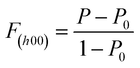
where P and P0 represent the ratio of the sum of diffraction intensities for the (h00) reflections to that of all the (hkl) reflections for the oriented sample and the standard PDF#48-1224 card, respectively. The closer F(h00) is to 1, the high texture of the sample is like that of single crystal.38,39 As summarized in Table 1, the F(400) values of the prepared SnSe0.95 + x mol% PbCl2 (x = 0, 4, 6, 8, 10) samples were 0.41, 0.48, 0.45, 0.49, and 0.46, respectively. These values are very close to that of the previously reported SnSe-based samples, indicating that our n-type SnSe0.95 + x mol% PbCl2 samples are preferentially oriented in the bc plane.

 | ||
| Fig. 1 The room-temperature XRD patterns of the SnSe0.95 + x mol% PbCl2 (x = 0, 4, 6, 8, and 10) samples (a) parallel and (b) perpendicular to the pressure direction. Typical SEM images of the x = 6 sample (c) parallel and (d) perpendicular to the pressure direction. | ||
| Sample | x = 0 | x = 4 | x = 6 | x = 8 | x = 10 |
|---|---|---|---|---|---|
| F (400) | 0.41 | 0.48 | 0.45 | 0.49 | 0.46 |
| ρ (g cm−3) | 6.040 | 6.141 | 6.156 | 6.200 | 6.237 |
As investigated in the previous milestone report, n-type SnSe exhibits the out-of-plane 3D electron transport and 2D phonon transport behavior.40 That is to say, the out-of-plane thermoelectric performance of n-type SnSe is higher than that in the bc plane. Considering that the oriented bc plane of our sample is parallel to the hot-pressing direction, in the following discussions we focus on the thermoelectric transport properties parallel to the pressure direction.
Fig. 2(a) shows the temperature-dependent electrical conductivity of the SnSe0.95 + x mol% PbCl2 (x = 0, 4, 6, 8, and 10) samples. It is found that the electrical conductivity monotonously increases with rising temperature, indicating an intrinsic semiconducting behavior.41 Compared with the pristine SnSe0.95, the electrical conductivities of PbCl2-doped SnSe0.95 samples are obviously improved in the measured temperature range, especially at higher temperatures (T > 650 K) owing to the thermal excitation of the carriers.31 For instance, the electrical conductivity of the 10% PbCl2-doped sample reaches 47.5 S cm−1 at 823 K, which is 5.5 times higher than that of the undoped SnSe0.95.
 | ||
| Fig. 2 Temperature dependence of the electronic transport coefficients parallel to the pressure direction for the SnSe0.95 + x mol% PbCl2 (x = 0, 4, 6, 8, and 10) sample: (a) electrical conductivity, (c) Seebeck coefficient, and (d) power factor. (b) Carrier concentration and mobility as functions of the PbCl2 content at 300 K. | ||
As presented in Fig. 2(b), the carrier concentration significantly increases with the amount of PbCl2 doping. For instance, the carrier concentration of 5.3 × 1019 cm−3 for the 10% PbCl2-doped samples is 200 times more than that of the undoped SnSe0.95 (2.6 × 1017 cm−3). The obtained carrier concentration is much higher than those of previously reported PbSe-SnCl2 co-doped samples by spark plasma sintering.42 This observation demonstrates that Pb and Cl doping at a ratio of 1:2 is effective to achieve higher carrier concentrations. The variation of the room-temperature electrical conductivities of SnSe0.95 + x mol% PbCl2 samples can be explained by the changed carrier concentrations and carrier mobilities. That is, the rise of electrical conductivity from 0.03 S cm−1 for the undoped sample to 1.98 S cm−1 for the 6% PbCl2-doped sample is derived from the boosted carrier concentration, and the subsequent fall to 1.42 S cm−1 for the 10% PbCl2 doped sample is due to the decreased carrier mobility.
Fig. 2(c) shows the Seebeck coefficient versus temperature for the SnSe0.95 + x mol% PbCl2 (x = 0, 4, 6, 8 and 10) samples. As may be seen, the pristine SnSe0.95 exhibits a p-type positive Seebeck coefficient at a lower temperature and an n-type negative Seebeck coefficient at a higher temperature. The p–n transition is realized in SnSe0.95 with a 5% Se deficiency. With PbCl2 doping, the Seebeck coefficients of all the SnSe0.95 + x mol% PbCl2 samples are negative, indicating an n-type conduction. The absolute values of the Seebeck coefficient of these PbCl2-doped SnSe0.95 samples monotonously increase with rising temperature. At a certain temperature, the absolute values of the Seebeck coefficient slightly decrease with the increasing PbCl2 content, mainly caused by the increased carrier concentration.
The power factors of the SnSe0.95 + x mol% PbCl2 (x = 0, 4, 6, 8 and 10) samples are plotted as a function of temperature in Fig. 2(d). Owing to the increased electrical conductivity and increased absolute value of the Seebeck coefficient, the power factor significantly increases with rising temperature, especially at temperatures above 550 K. With the highest absolute value of the Seebeck coefficient and moderate electrical conductivity, the x = 6 sample exhibits the highest power factor, 7.33 μW·cm−1 K−2 at 823 K.
Fig. 3(a) shows the total thermal conductivity of the SnSe0.95 + x mol% PbCl2 (x = 0, 4, 6, 8 and 10) samples from 300 to 823 K. It is found that κ firstly decreases with rising temperature, reaches a minimum value around 750 K, and then slightly increases. The increased κ at a higher temperature may result from the excited bipolar effect, which was also found in a previous report.43,44 At a certain temperature, κ of PbCl2-doped SnSe0.95 firstly decreases with an increasing content of PbCl2, reaches a minimum value with 6% PbCl2 doping, and then slightly increases. For instance, the total thermal conductivity at room temperature decreases from 1.2 W m−1 K−1 for the undoped SnSe0.95 to 0.85 W m−1 K−1 for SnSe0.95 + 6% PbCl2.
 | ||
| Fig. 3 Temperature-dependent (a) total thermal conductivity, (b) electronic thermal conductivity, (c) lattice thermal conductivity, and (d) ZT value for SnSe0.95 + x mol% PbCl2 (x = 0, 4, 6, 8, and 10) parallel to the pressure direction. | ||
Fig. 3(b) plots the electronic thermal conductivity as a function of temperature. κe is obtained according to the Wiedemann–Franz law, κe = LσT, where L is the Lorentz constant and evaluated as L = 1.5 + exp(−|S|/116).45 The temperature dependence of the electronic thermal conductivity is similar to that of the electrical conductivity in Fig. 2(a).
Fig. 3(c) shows the lattice thermal conductivity κl as a function of temperature, which is obtained by subtracting the electronic contribution κe from the total thermal conductivity κ. Since the electronic thermal conductivity contributes a small proportion of the total thermal conductivity, the temperature dependence of lattice thermal conductivity is almost the same as that of the total thermal conductivity. The lowest lattice thermal conductivity is 0.49 W m−1 K−1, obtained in the 6% PbCl2-doped SnSe0.95 at 752 K. Except at temperatures higher than 750 K, the lattice thermal conductivities of the PbCl2-doped SnSe0.95 samples are lower than that of the undoped SnSe0.95, indicating that the lead compound doping can effectively suppress the lattice thermal conductivity of tin selenide.40
To further explore the underlying physical mechanism of the low lattice thermal conductivity in PbCl2-doped SnSe0.95, we used a TEM technique to observe and analyze the microscopic structure of the 6% PbCl2-doped sample. Fig. 4(a) is a bright-field TEM image, where grain boundaries (marked by an orange dotted line), dislocation nets (marked by a blue dotted circle), and dislocations (marked by blue triangles) can be observed. Fig. 4(b) is a high-resolution TEM of the grain boundary area marked by the white dotted box in Fig. 4(a), and it shows the orthorhombic SnSe lattice and the (400) plane with a spacing of 2.87 Å. Fig. 4(c) is an inverse fast Fourier transformation plot for the orange dotted box area in the high-resolution TEM image of Fig. 4(b), and the dislocations are marked as a red “⊥” in Fig. 4(c). A microregion quantitative EDS elemental mapping analysis was adopted to illustrate the homogeneous distribution of Sn, Pb, Cl and Se, as shown in Fig. 4(d), and is consistent with the above XRD results. Besides the point defects of PbCl2 doping, the grain boundaries and induced dislocations can also enhance the phonon scattering, and they are all responsible for the suppression of the lattice thermal conductivity of SnSe0.95-based materials.
 | ||
| Fig. 4 TEM images for the SnSe0.95 + 6 mol% PbCl2 sample: (a) a bright-field TEM image shows grain boundaries and dislocations, (b) a high-resolution TEM image, (c) an inverse fast Fourier transformation image for the marked orange area in (b) to show the dislocations, and (d) the elemental distribution for Sn, Se, Pb, and Cl. | ||
The ZT values for the SnSe0.95 + x mol% PbCl2 (x = 0, 4, 6, 8, and 10) samples parallel to the pressure direction are plotted in Fig. 3(d) as a function of temperature. Since PbCl2 doping boosts the carrier concentration to improve the power factor and enhances the phonon scattering to reduce the lattice thermal conductivity, all the PbCl2-doped samples exhibit a higher ZT than that of the undoped SnSe0.95 control sample. With the highest power factor of 7.33 μW cm−1 K−2 and lowest lattice thermal conductivity of 0.45 W m−1 K−1, the x = 6 sample realizes a maximum ZT of 1.13 at 823 K. Although a ZT value of 1.13 is lower than that of the n-type SnSe0.95 single crystal, it is still competitive with those of other polycrystalline halide-doped SnSe0.95 systems.11,30,46
Conclusions
In summary, we successfully prepared the n-type polycrystalline SnSe0.95 + x mol% PbCl2 (x = 0, 4, 6, 8, and 10) samples by a hot-pressing method. The XRD result shows that the prepared samples exhibit a strong orientation along the (400) plane. The Hall measurement suggests that PbCl2 is sufficient to boost the carrier concentration, leading to an obviously improved electrical conductivity and power factor. Moreover, the microstructure investigation indicates that the induced grain boundaries, dislocations, and point defects by PbCl2 doping suppress the lattice thermal conductivity. As a consequence, a maximum ZT value of 1.13 is obtained in the SnSe0.95 + 6% PbCl2 sample. This work provides a viable strategy for the future optimization of n-type SnSe-based thermoelectric materials.Conflicts of interest
There are no conflicts of interest to declare.Acknowledgements
This work was supported by the National Natural Science Foundation of China (52002382).References
- M. S. Dresselhaus, G. Chen, M. Y. Tang, R. G. Yang, H. Lee, D. Z. Wang, Z. F. Ren, J. P. Fleurial and P. Gogna, Adv. Mater., 2007, 19, 1043–1053 CrossRef CAS.
- X. L. Su, P. Wei, H. Li, W. Liu, Y. G. Yan, P. Li, C. Q. Su, C. J. Xie, W. Y. Zhao, P. C. Zhai, Q. J. Zhang, X. F. Tang and C. Uher, Adv. Mater., 2017, 29, 1602013 CrossRef PubMed.
- Y. M. Zhou and L. D. Zhao, Adv. Mater., 2017, 29, 1702676 CrossRef PubMed.
- G. J. Snyder and E. S. Toberer, Nat. Mater., 2008, 7, 105–114 CrossRef CAS PubMed.
- L. E. Bell, Science, 2008, 321, 1457–1461 CrossRef CAS PubMed.
- S. B. Riffat and X. L. Ma, Appl. Therm. Eng., 2003, 23, 913–935 CrossRef.
- X. Zhang and L. D. Zhao, J. Materiomics, 2015, 1, 92–105 CrossRef.
- L. D. Zhao, C. Chang, G. J. Tan and M. G. Kanatzidis, Energy Environ. Sci., 2016, 9, 3044–3060 RSC.
- G. Han, Z. G. Chen, J. Drennan and J. Zou, Small, 2014, 10, 2747–2765 CrossRef CAS PubMed.
- A. T. Duong, V. Q. Nguyen, G. Duvjir, V. T. Duong, S. Kwon, J. Y. Song, J. K. Lee, J. E. Lee, S. D. Park, T. Min, J. Lee, J. Kim and S. Cho, Nat. Commun., 2016, 7, 13713 CrossRef CAS PubMed.
- X. Wang, J. T. Xu, G. Q. Liu, Y. J. Fu, Z. Liu, X. J. Tan, H. Z. Shao, H. C. Jiang, T. Y. Tan and J. Jiang, Appl. Phys. Lett., 2016, 108, 083902 CrossRef.
- A. Banik, U. S. Shenoy, S. Anand, U. V. Waghmare and K. Biswas, Chem. Mater., 2015, 27, 581–587 CrossRef CAS.
- M. Hong, Z. G. Chen, L. Yang, Y. C. Zou, M. S. Dargusch, H. Wang and J. Zou, Adv. Mater., 2018, 30, 1705942 CrossRef PubMed.
- M. Hong, Z. G. Chen, L. Yang, T. C. Chasapis, S. D. Kang, Y. C. Zou, G. J. Auchterlonie, M. G. Kanatzidis, G. J. Snyder and J. Zou, J. Mater. Chem. A, 2017, 5, 10713–10721 RSC.
- W. Liu, X. J. Tan, K. Yin, H. J. Liu, X. F. Tang, J. Shi, Q. J. Zhang and C. Uher, Phys. Rev. Lett., 2012, 108, 166601 CrossRef PubMed.
- G. J. Tan, L. D. Zhao and M. G. Kanatzidis, Chem. Rev., 2016, 116, 12123–12149 CrossRef CAS PubMed.
- L. D. Zhao, S. H. Lo, Y. S. Zhang, H. Sun, G. J. Tan, C. Uher, C. Wolverton, V. P. Dravid and M. G. Kanatzidis, Nature, 2014, 508, 373–377 CrossRef CAS PubMed.
- S. Chandra, U. Bhat, P. Dutta, A. Bhardwaj, R. Datta and K. Biswas, Adv. Mater., 2022, 34, 2203725 CrossRef CAS PubMed.
- Z. G. Chen, X. L. Shi, L. D. Zhao and J. Zou, Prog. Mater. Sci., 2018, 97, 283–346 CrossRef CAS.
- C. W. Li, J. Hong, A. F. May, D. Bansal, S. Chi, T. Hong, G. Ehlers and O. Delaire, Nat. Phys., 2015, 11, 1063–1069 Search PubMed.
- Y. Xiao, C. Chang, Y. L. Pei, D. Wu, K. L. Peng, X. Y. Zhou, S. K. Gong, J. Q. He, Y. S. Zhang, Z. Zeng and L. D. Zhao, Phys. Rev. B, 2016, 94, 125203 CrossRef.
- Y. Liu, M. Calcabrini, Y. Yu, S. Lee, C. Chang, J. David, T. Ghosh, M. C. Spadaro, C. Y. Xie, O. Cojocaru-Mirédin, J. Arbiol and M. Ibáñez, ACS Nano, 2022, 16, 78–88 CrossRef CAS PubMed.
- S. Chandra, P. Dutta and K. Biswas, ACS Nano, 2022, 16, 7–14 CrossRef CAS PubMed.
- H. X. Liu, S. Zhang, Y. Zhang, S. T. Zong, W. Li, C. Zhu, F. Luo, J. Wang and Z. G. Sun, ACS Appl. Energy Mater., 2022, 5, 15093–15101 CrossRef CAS.
- Y. X. Chen, Z. H. Ge, M. J. Yin, D. Feng, X. Q. Huang, W. Y. Zhao and J. Q. He, Adv. Funct. Mater., 2016, 26, 6836–6845 CrossRef CAS.
- Z. H. Ge, D. S. Song, X. Y. Chong, F. S. Zheng, L. Jin, X. Qian, L. Zheng, R. E. Dunin-Borkowski, P. Qin, J. Feng and L. D. Zhao, J. Am. Chem. Soc., 2017, 139, 9714–9720 CrossRef CAS PubMed.
- J. R. Li, J. T. Xu, H. X. Wang, G. Q. Liu, X. J. Tan, H. Z. Shao, H. Y. Hu and J. Jiang, J. Mater. Sci.: Mater. Electron., 2018, 29, 18727–18732 CrossRef CAS.
- J. Liu, P. Wang, M. Y. Wang, R. Xu, J. Zhang, J. Z. Liu, D. Li, N. N. Liang, Y. W. Du, G. Chen and G. D. Tang, Nano Energy, 2018, 53, 683–689 CrossRef CAS.
- G. Han, S. R. Popuri, H. F. Greer, L. F. Llin, J. G. Bos, W. Z. Zhou, D. J. Paul, H. Ménard, A. R. Knox, A. Montecucco, J. Siviter, E. A. Man, W. G. Li, M. C. Paul, M. Gao, T. Sweet, R. Freer, F. Azough, H. Baig, T. K. Mallick and D. H. Gregory, Adv. Energy Mater., 2017, 7, 1602328 CrossRef.
- D. B. Li, X. J. Tan, J. T. Xu, G. Q. Liu, M. Jin, H. Z. Shao, H. J. Huang, J. F. Zhang and J. Jiang, RSC Adv., 2017, 7, 17906–17912 RSC.
- C. Chang, Q. Tan, Y. L. Pei, Y. Xiao, X. Zhang, Y. X. Chen, L. Zheng, S. K. Gong, J. F. Li, J. Q. He and L. D. Zhao, RSC Adv., 2016, 6, 98216–98220 RSC.
- S. Li, Y. M. Wang, C. Chen, X. F. Li, W. H. Xue, X. Y. Wang, Z. W. Zhang, F. Cao, J. H. Sui, X. J. Liu and Q. Zhang, Adv. Sci., 2018, 5, 1800598 CrossRef PubMed.
- L. S. Mao, Y. N. Yin, Q. Zhang, G. Q. Liu, H. X. Wang, Z. Guo, H. Y. Hu, Y. K. Xiao, X. J. Tan and J. Jiang, Energy Environ. Sci., 2020, 13, 616–621 RSC.
- Q. Zhang, E. K. Chere, J. Y. Sun, F. Cao, K. Dahal, S. Chen, G. Chen and Z. F. Ren, Adv. Energy Mater., 2015, 5, 1500360 CrossRef.
- A. Das, A. Chauhan, V. Trivedi, M. Tiadi, R. Kumar, M. Battabyal and D. K. Satapathy, Phys. Chem. Chem. Phys., 2021, 23, 4230–4239 RSC.
- X. L. Shi, J. Zou and Z. G. Chen, Chem. Rev., 2020, 120, 7399–7515 CrossRef CAS PubMed.
- X. Y. Mao, X. L. Shi, L. C. Zhai, W. D. Liu, Y. X. Chen, H. Gao, M. Li, D. Z. Wang, H. Wu, Z. H. Zheng, Y. F. Wang, Q. F. Liu and Z. G. Chen, J. Mater. Sci. Technol., 2022, 114, 55–61 CrossRef.
- W. H. Gu, Y. X. Zhang, J. Guo, J. F. Cai, Y. K. Zhu, F. S. Zheng, L. Jin, J. T. Xu, J. Feng and Z. H. Ge, J. Alloys Compd., 2021, 864, 158401 CrossRef CAS.
- F. Li, W. T. Wang, Z. H. Ge, Z. H. Zheng, J. T. Luo, P. Fan and B. Li, Materials, 2018, 11, 203–213 CrossRef PubMed.
- L. Z. Su, D. Y. Wang, S. N. Wang, B. C. Qin, Y. P. Wang, Y. X. Qin, Y. Jin, C. Chang and L. D. Zhao, Science, 2022, 375, 1385–1389 CrossRef CAS PubMed.
- H. X. Wang, H. Y. Hu, N. Man, C. L. Xiong, Y. K. Xiao, X. J. Tan, G. Q. Liu and J. Jiang, Mater. Today Phys., 2021, 16, 100298 CrossRef CAS.
- J. Cha, C. J. Zhou, Y. K. Lee, S. P. Cho and I. Chung, ACS Appl. Mater. Interfaces, 2019, 11, 21645–21654 CrossRef CAS PubMed.
- N. Xin, Y. F. Li, H. Shen, L. Y. Shen and G. H. Tang, J. Materiomics, 2022, 8, 475–488 CrossRef.
- S. Chandra, U. Bhat, P. Dutta, A. Bhardwaj, R. Datta and K. Biswas, Adv. Mater., 2022, 34, 2203725 CrossRef CAS PubMed.
- J. F. Cai, Y. Zhang, Y. N. Yin, X. J. Tan, S. C. Duan, G. Q. Liu, H. Y. Hu, Y. K. Xiao, Z. H. Ge and J. Jiang, J. Mater. Chem. C, 2020, 8, 13244–13252 RSC.
- T. Shen, K. Y. Li, Z. J. Chen, H. F. Wu and J. X. Si, J. Electron. Mater., 2019, 49, 621–626 CrossRef.
| This journal is © The Royal Society of Chemistry 2023 |