
 Open Access Article
 This Open Access Article is licensed under a Creative Commons Attribution-Non Commercial 3.0 Unported Licence
Chloride-assisted synthesis of tellurene directly on SiO2/Si substrates: growth mechanism, thermal properties, and device applications†
Yi-Hsun
Chan
a,
Che-Yi
Lin
b,
Yu-Chang
Chou
a,
Alice Chinghsuan
Chang
 g,
Yen-Fu
Lin
bdef and
Yu-Ze
Chen
*ac
g,
Yen-Fu
Lin
bdef and
Yu-Ze
Chen
*ac
aDepartment of Materials Science and Engineering, National Cheng Kung University, Tainan City, 70101, Taiwan. E-mail: yzchen@gs.ncku.edu.tw
bDepartment of Physics, National Chung Hsing University, Taichung 40227, Taiwan
cProgram on Key Materials, Academy of Innovative Semiconductor and Sustainable Manufacturing, National Cheng Kung University, Tainan City, 70101, Taiwan
dDepartment of Materials Science and Engineering, National Chung Hsing University, Taichung 40227, Taiwan
eInstitute of Nanoscience, National Chung Hsing University, Taichung 40227, Taiwan
fi-Center for Advanced Science and Technology (i-CAST), National Chung Hsing University, Taichung 40227, Taiwan
gCenter for Measurement Standards, Industrial Technology Research Institute, Hsinchu, 30011, Taiwan
First published on 21st March 2023
Abstract
The new single-element two-dimensional materials in the post-graphene era, such as phosphorene and silicene, are emerging as alternative next-generation materials due to their remarkable physical properties. However, the vulnerability of silicene and phosphorene to the air hinders their practical applications. Recently, a new kind of single-element two-dimensional material, namely tellurene, exhibiting outstanding electrical mobility and superior long-term stability in the air, has been successfully synthesized. Here, we report that the addition of chloride (TeCl4) to TeO2 is conducive to the lateral growth of tellurium on the SiO2/Si substrate. The resulting tellurene flakes display outstanding structure stability over 30 days under ambient exposure. Furthermore, the applicability of SThM (scanning thermal microscopy) to investigate the thermal properties of tellurene is presented for the first time, revealing its abnormal thermal conductance across grain boundaries and a thickness-dependent thermal transport behavior. Finally, tellurene-based FETs (field effect transistors) were fabricated, which displayed temperature-dependent Ids that decreased with decreasing temperature rather than metallic transport features, which implies thermal activation of a semiconductor and confirms that the transport follows the 2D variable-range hopping (VRH) model.
Introduction
In 2005, for the first time, scientists successfully exfoliated a single layer of graphite, known as graphene, which surprisingly exhibited superior properties in all aspects, such as outstanding catalytic ability,1,2 high transparency with high conductivity,3 and high electrical mobility at room temperature, as well as long-term stability in air.4,5 For over a decade, scientists have drawn their attention away from graphene due to its major shortcoming of zero bandgap, which hinders its application in logics.6 Two dimensional transition metal dichalcogenides (TMDCs) have unfolded another vigorous research trend because of the inherent nature of their bandgap, which yields great potential for developing next-generation electronic devices. However, the current state-of-the-art TMDC-based transistors are barely satisfactory in terms of electron mobility, which is still far below that of the modern Si-based transistor. Recently, the widely and intensively investigated single-element two-dimensional materials made of graphene derivatives have exhibited intriguing photoelectric properties,7 energy-storage ability,8 and ultra-high electron mobility.9 Tellurium, which belongs to the chalcogens, possesses a unique chiral crystal structure, in which the atoms in a chain are bonded with the neighboring atoms by covalent bonding, and the two adjacent chains are attracted by van der Waals forces. Since 2004, the anisotropy in the atomic structure of Te has led to the limitation of its study and applications that are mainly based on the nanowire at the early stage of development.10 Tellurene (two-dimensional Te) has become one of the emerging two-dimensional materials because of its intriguing optical,11,12 magnetic13,14 and thermal properties.15–17 Recently, scientists have made great progress toward the synthesis of the lamellar structure of Te, called tellurene, by the substrate-free hydrothermal approach,18,19 low-temperature deposition via the PVD (physical vapor deposition) process on Si20 and epitaxial growth on a single crystalline substrate via CVD (chemical vapor deposition).21 Y. Wang et al. have proposed a reliable solution for achieving the large-scale synthesis of tellurene with high crystallinity and also fabricated tellurene-based FETs (field effect transistors), displaying a high on/off ratio of 1 × 10⁵ with excellent hole mobility (∼700 cm2 V−1 s−1). More strikingly, their most important finding is the ultra-long structural stability (∼55 days) without any protective layer upon exposure to the air. However, the inert chemical activity and high anisotropy in the structure of tellurium render the process of obtaining lamellar tellurium with a much thinner thickness considerably time-consuming (up to 50 hours).18 X. Zhang et al. conducted the reduction of TeO2 by simply using hydrogen to allow epitaxial deposition on the basal plane of mica. Additionally, through DFT calculations, they found that the intermediates played a critical role in the formation of tellurene. In addition, the usage of a single-crystalline substrate for the epitaxial growth of tellurene was inevitable.21–23 Hence, the synthesis of tellurene directly on an amorphous substrate for wider application still remains a challenge.Herein, we propose a reliable method for synthesizing tellurium on arbitrary substrates and have discovered the influence of the ratio of TeCl4/TeO2 on the dimension of the resulting products, from one-dimensional to two-dimensional structure. Choosing precursors with low-melting points enables the direct synthesis of Te nanoflakes on arbitrary substrates, such as sapphire, mica and SiO2/Si wafer. In addition, a systematic investigation of growth parameters during the formation of tellurene was conducted. As a result, the essential factors that determine the preferential growth direction of Te are proposed here, for the first time.
Results and discussion
Fig. 1(a) depicts the experimental setup of the CVD process, in which the precursors TeO2/TeCl4 were placed in the upstream region (750 °C), and the SiO2/Si substrate was placed in the downstream region (750 °C) 30 cm away from the precursors for the deposition of Te. Once the process was completed, several single crystals were found loosely spread on the substrate (Fig. 1(b)), and the magnified images reflected light-pink hexagonal flakes (see the inset of Fig. 1(b)). Next, the thickness and dimension of the resulting materials were confirmed by AFM (atomic force microscope) to be around 10 nm (Fig. 1(c)). Note that if the thickness of tellurene was greater than 50 nm, it appeared the shiny golden, reflecting the metalloid innate. Since the discovery of graphene, Raman spectroscopy has been regarded as a helpful technique, especially, for the analysis of the vibration modes of two-dimensional materials and even the estimation of their thickness. Fig. 1(d) presents the typical spectrum of tellurene. The two featured peaks of the A1 mode (123 cm−1) and E2 mode (140 cm−1) were detected in accordance with previous reports, confirming the successful formation of tellurene. Remarkably, along with the increase in the thickness of tellurene, the signal from the substrate gradually vanished. Furthermore, it was discovered that the Raman peaks of the A1 mode, which are associated with the vibration of the intrachain of Te, exhibited a redshift as the thickness of tellurene increased. This indicates that the van der Waals forces are influenced by thickness, resulting in the frequency change of the intra-chain vibrations. | ||
| Fig. 1 Material characterization of tellurene. (a) Experimental setup of the CVD process, in which the hybrid precursors TeO2/TeCl4 are placed in the upper stream, and the SiO2/Si substrate is placed 30 cm away from the precursors. (b) The optical image of the hexagonal tellurene flakes. (c) The AFM image confirming the thickness of tellurene to be around 10.3 nm. (d) The Raman spectrum of tellurene consists of peaks at 123 cm−1 and 140 cm−1, which correspond to the A1 mode and E2 mode, respectively. | ||
In order to identify the atomic structure of tellurene, high-resolution TEM (transmission electron microscopy) was exploited. Prior to TEM observation, tellurene was capped with SiO2 for protection from damage by the Ar+ ions during the FIB (focused ion beam) process, as shown in Fig. 2(a). Fig. 2(b) displays the cross-sectional TEM image, clearly revealing the layered structure with a spacing of 3.9 Å, which matches the values in previous reports,22,24 and the preferential epitaxial direction corresponding to the (001) plane (Fig. 2(c)). Next, based on the compositional analysis by TEM-EDX, the element mapping showed that the signal Te was uniformly distributed, and the interface between Te and SiO2 was sharply divided, as shown in Fig. 2(d1–d4). Considering the structural stability of tellurene in the air, the TEM sample of tellurene prepared by FIB was intentionally placed in the air for 30 days. After cross-sectional cutting by FIB, the edge of tellurene was fully exposed to the air, and the edge of the two-dimensional material confirmed that was susceptible to the air.25 After that, TEM was applied for the estimation of its stability in the air. Significantly, the layered structure was still observed with no evident degradation, as shown in Fig. 2(e1–f2). The long duration of stability up to around 30 days evidently exceeds that of silicene which is stable for 48 min,19 and that of phosphorene, which is stable for 60 min.26
 | ||
| Fig. 2 TEM characterization and the structural stability test. (a) The cross-sectional image of tellurene. (b) The magnified view of 10.5 nm tellurene, revealing the layered structure with a lattice spacing of 3.9 Å. (c) SAED pattern. (d1–d4) The TEM-EDX mapping images of Te, O and Si, respectively. (e1) The cross-sectional image of fresh tellurene and (e2) the corresponding SAED pattern. (f1) The cross-sectional image of tellurene exposed to the air for over 30 days and (f2) the corresponding SAED pattern. | ||
To understand the role of the gas species during the synthesis of tellurene, the gas mixture of Ar/H2 at varied ratios was investigated and the ratio of precursor TeO2/TeCl4 was set to 10 g/30 g. When pure Ar gas was used through the process, no tellurene flakes were observed, and only dark particles were spread on the surface (Fig. 3(a1)). Next, the hydrogen was introduced at a constant total flow flux of (Ar + H2 = 15 sccm), and it was found to participate in the reaction of TeO2/TeCl4. Once the hydrogen was introduced, hexagonal flakes appeared on the surface (Fig. 3(a2)). While increasing the amount of hydrogen to 8 sccm or 15 sccm, the color of the resulting flakes obviously turned from yellow to pink (Fig. 3(a3 and a4)). Fig. 3(a5) plots the dependence of the lateral dimension and thickness of the flakes on the Ar/H2 ratio. It is worth noting that the thickness of tellurene was inversely proportional to the proportion of hydrogen, which is possible due to the etching effect, as observed in previous works on graphene synthesis, proving that hydrogen could thin down the resultant thickness.27 The thinnest value realized in this work was around 12 nm with pure hydrogen. Moreover, the total amount of hydrogen affected the dimension and thickness of tellurene (Fig. S1, ESI†). The process temperature was set to 750 °C and maintained for 30 min. When the flux of hydrogen was 5 sccm, there was no deposition of tellurene due to the insufficient carrier gas to deliver the Te vapor. When the flux was increased to 10 sccm, tellurene flakes with a thickness of 20 nm were achieved, but the dimension was irregular. When the flux was increased to 15 sccm, regular hexagonal tellurene flakes were realized. It is worth mentioning that when the flux was over 20 sccm, thicker tellurene flakes (∼56.7 nm in thickness) were obtained, which can be attributed to the tendency of the excess Te vapor to nucleate on the existing Te flakes, resulting in the overlapping of multiple flakes.28 Different from the previous works on tellurene synthesis through the simple reduction of TeO2 with the assistance of hydrogen,21 in this work, low-melting-point TeCl4 (melting point: 230 °C) is also chosen as another Te feedstock. It was found that the ratio of TeO2/TeCl4 played a decisive role in the growth mechanism during the transition from one-dimensional nanowire to two-dimensional epitaxial growth. Contrary to previous works,21 which solely use TeO2 as the precursor for the reduction reaction using hydrogen, it was hard to synthesize tellurene thin films, but only less bulky Te with an irregular shape was found on the SiO2/Si substrate (Fig. 3(b1)), as confirmed by SEM and Raman examination (Fig. S2(a1 and a2), ESI†). It was speculated that since the process temperature (750 °C) was slightly above the melting point of TeO2 (733 °C), only a limited amount of TeO2 would have melted, resulting in Te vapor deficiency. Whereas, while solely using TeCl4 as the precursor, one-dimensional nanorods were realized, as shown in Fig. S2(b1 and b2) (ESI†), revealing the tendency of its growth along the Z-axis because of the highly anisotropic bonding strength, in accordance with the previous works on synthesizing Te nanowires.29,30 It is expected that the low-melting-point TeCl4 (230 °C) will be easily evaporated and quickly form a saturated vapor. Meanwhile, when reacted with H2, the TeCl4 vapor was reduced to Te vapor. Hence, as the temperature gradually increased, the reduction of TeCl4 by hydrogen became more intense, resulting in an increase in nucleation probability on the SiO2/Si substrate. Moreover, the Te vapor preferably tended to accumulate on the existing nucleation sites, leading to one-dimensional nanowire growth.31 Herein, the influence of the precursor ratio of TeO2/TeCl4 on the growth mechanism was elucidated. At a ratio of TeO2/TeCl4 = 10![[thin space (1/6-em)]](https://www.rsc.org/images/entities/char_2009.gif) :10 mg, hexagonal flakes were synthesized on the SiO2/Si substrate perfectly (Fig. 3(b2)), and the lateral size increased with the amount of TeCl4 (Fig. 3(b3)). With excessive TeCl4 over 50 mg, the color obviously turned shiny golden (Fig. 3(b4)). Moreover, upon increasing the amount of TeCl4 from 10 to 30 and 50 mg, obviously the density of tellurene increased from 2 μm−2 to 50 μm−2, which can be attributed to the increasing Te vapor, which is beneficial to initial nucleation for subsequent growth (Fig. S3, ESI†). Finally, the dependence of the ratio of TeO2/TeCl4 on the lateral size and thickness was plotted, as shown in Fig. 3(b5), which displays that the thickness greatly increased from 12 nm to 70 nm while the lateral size did not undergo great changes (Fig. 3(b5)). The strong tendency toward an increase in thickness with the increasing amount of TeCl4 yielded a preferential vertical growth, which is in accordance with previous works on the synthesis of one-dimensional nanowires by using TeCl4 as the Te source.32 Hence, by precisely controlling the ratio of TeO2/TeCl4, it is possible to manipulate the growth mechanism of tellurene from one-dimensional nanowire to two-dimensional tellurene. In addition, the process temperature has a great influence on the thickness of tellurene, as shown in Fig. S4 (ESI†). It was found that tellurene could not be synthesized when the process temperature was 680 °C. However, when the temperature reached 720 °C, hexagonal Te flakes formed on the SiO2/Si substrate successfully. When the process temperature was elevated to 750 °C, the lateral size of tellurene increased to 8 μm. However, when the process temperature was elevated to 780 °C, the thickness increased from 12 nm to 90 nm, implying that the excessive Te vapor preferably led to epitaxial growth along the Z-axis. Therefore, the growth window of tellurene is considerably narrow and significantly correlates with the ratio of TeO2/TeCl4, the gas mixture of Ar/H2, and the process temperature.
:10 mg, hexagonal flakes were synthesized on the SiO2/Si substrate perfectly (Fig. 3(b2)), and the lateral size increased with the amount of TeCl4 (Fig. 3(b3)). With excessive TeCl4 over 50 mg, the color obviously turned shiny golden (Fig. 3(b4)). Moreover, upon increasing the amount of TeCl4 from 10 to 30 and 50 mg, obviously the density of tellurene increased from 2 μm−2 to 50 μm−2, which can be attributed to the increasing Te vapor, which is beneficial to initial nucleation for subsequent growth (Fig. S3, ESI†). Finally, the dependence of the ratio of TeO2/TeCl4 on the lateral size and thickness was plotted, as shown in Fig. 3(b5), which displays that the thickness greatly increased from 12 nm to 70 nm while the lateral size did not undergo great changes (Fig. 3(b5)). The strong tendency toward an increase in thickness with the increasing amount of TeCl4 yielded a preferential vertical growth, which is in accordance with previous works on the synthesis of one-dimensional nanowires by using TeCl4 as the Te source.32 Hence, by precisely controlling the ratio of TeO2/TeCl4, it is possible to manipulate the growth mechanism of tellurene from one-dimensional nanowire to two-dimensional tellurene. In addition, the process temperature has a great influence on the thickness of tellurene, as shown in Fig. S4 (ESI†). It was found that tellurene could not be synthesized when the process temperature was 680 °C. However, when the temperature reached 720 °C, hexagonal Te flakes formed on the SiO2/Si substrate successfully. When the process temperature was elevated to 750 °C, the lateral size of tellurene increased to 8 μm. However, when the process temperature was elevated to 780 °C, the thickness increased from 12 nm to 90 nm, implying that the excessive Te vapor preferably led to epitaxial growth along the Z-axis. Therefore, the growth window of tellurene is considerably narrow and significantly correlates with the ratio of TeO2/TeCl4, the gas mixture of Ar/H2, and the process temperature.
 | ||
| Fig. 3 Investigation of the gas ratio of Ar/H2 and the ratio of TeO2/TeCl4 precursors on the formation of tellurene. Tellurene formed in the presence of (a1) pure Ar 15 sccm, (a2) Ar/H2 = 12:3 (sccm), (a3) Ar/H2 = 7:8 (sccm), and (a4) pure H2 15 sccm. (a5) The dependence of the lateral dimension of tellurene on the gas ratio of Ar/H2, (b1) Pure TeO2, (b2) TeO2/TeCl4 = 10:10 (mg), (b3) TeO2/TeCl4 = 10:30 (mg), and (b4) TeO2/TeCl4 = 10:50 (mg). (b5) The dependence of the lateral dimension of tellurene on the ratio of TeO2/TeCl4. | ||
Moreover, with the aid of TeCl4, tellurene was not only successfully synthesized on the SiO2/Si substrate but also could be demonstrated on quartz, mica and sapphire (Fig. S5, ESI†).
Apparently, the thickness of tellurene on quartz was found to be much greater than that on other single crystalline substrates owing to the greater roughness, which would lead to the localization of the Te vapor, resulting in the intensive deposition of Te. In addition, the high density of hexagonal flakes spread on mica and sapphire is due to the high crystallinity and low roughness of the underlying substrates, which are beneficial to the epitaxial growth of tellurene.
Finally, the detailed growth mechanism of tellurium from bulk down to 1D and 2D controlled by the precursors TeCl4/TeO2 is well-established. It is worth mentioning that, while solely using TeO2 as the precursor, it was discovered that not only the products of the Te bulk but silver residues also remained in the boat wherein TeO2 was initially placed after the process (Fig. S6(a), ESI†); material characterization by Raman spectroscopy (Fig. S6(b), ESI†) confirmed the existence of α-TeO2.33 However, in the case of using the mixture of TeCl4/TeO2 as the Te precursors, no residues were observed (Fig. S6(c), ESI†), indicating that TeO2 was completely and effectively reduced to Te with the assistance of TeCl4. The routes of synthesizing tellurene are illustrated in Fig. 4(a). As the process temperature ramps up over the melting point of TeCl4 (230 °C), TeCl4 is dissociated into TeCl2 and Cl2,34 and reacts with H2. Eventually, the Te vapor is generated through the reduction reaction by H2 accompanied by the formation of the massive byproduct HCl.35 When the temperature approaches the melting point of TeO2 (733 °C), the TeO2 vapor reacts with HCl to form TeCl436 and H2O. These intermediate products successively react with H2 to generate the Te vapor as a result. It is worth noting that through DFT calculations, it has been proven that the intermediate H2O benefits the construction of the layered structure of Te.21 Such a high concentration of Te vapor mitigates the inert chemical reactivity itself, turning conducive to the formation of nucleation sites on the SiO2/Si substrate at the early stage. The chemical reaction involved in the deposition of Te can be divided into two steps.
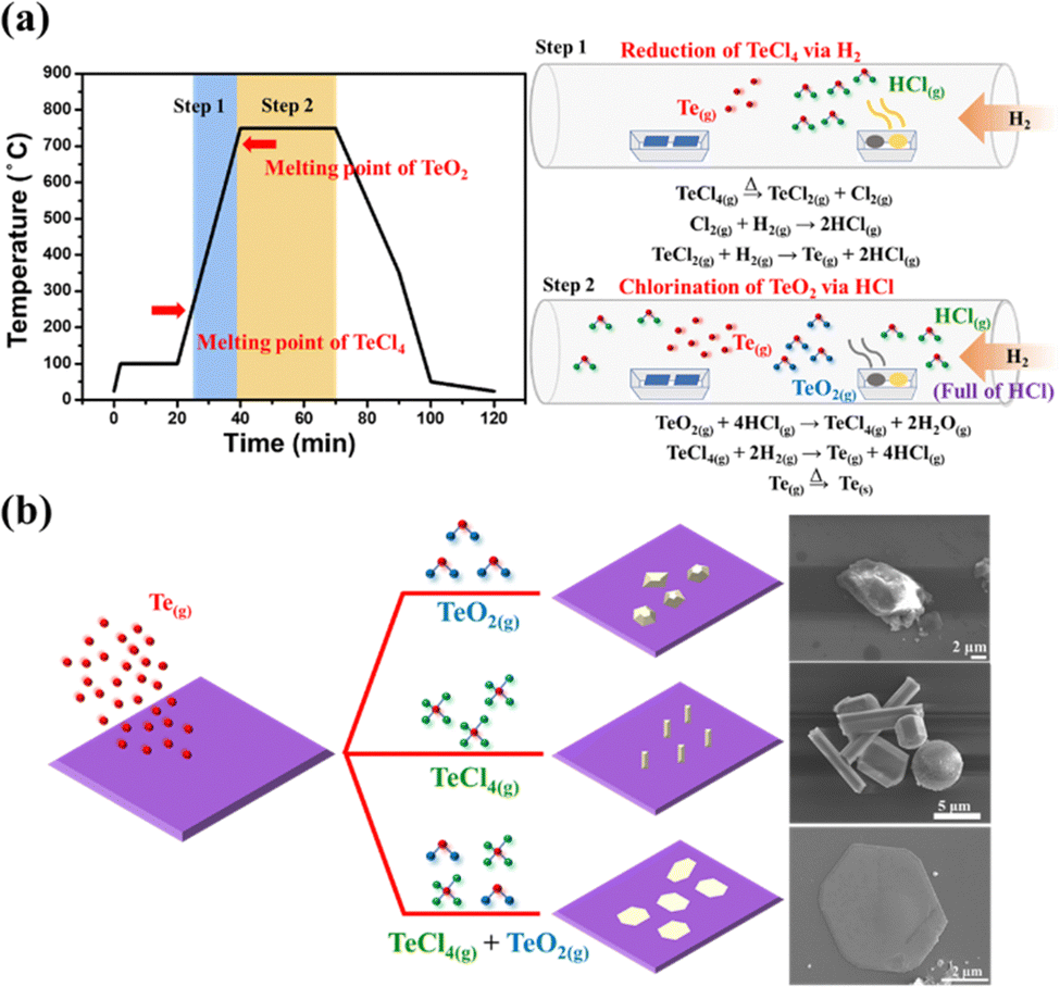 | ||
| Fig. 4 (a) The temperature profile of the CVD process corresponding to the two-step chemical reaction. Step 1: the reduction of TeCl4via H2; step 2: The chlorination of TeO2via HCl. (b) the reaction route of the formation of tellurene depending on the selection of precursors. | ||
Step 1: reduction of TeCl4 by H2
| TeCl4(g) → TeCl2(g) + Cl2(g) | (1) |
| Cl2(g) + H2 → 2HCl(g) | (2) |
| TeCl2(g) + H2(g) → Te(g) + 2HCl(g) | (3) |
Step 2: chlorination of TeO2 by HCl
| TeO2(g) + 4HCl(g) → TeCl4(g) + 2H2O(g) | (4) |
| TeCl4(g) + 2H2(g) → Te(g) + 4HCl(g) | (5) |
| Te(g) → Te(s) | (6) |
Nevertheless, with the addition of low-melting-point TeCl4 with TeO2 as Te precursors, hexagonal flakes of tellurene are successfully synthesized on the SiO2/Si substrate due to the f high saturated vapor pressure achieved by the addition of low-melting chloride. Hence, it is speculated that the consistent supply of Te feedstocks is essential to overcome the inherent limitation in growth direction imposed by the high anisotropy in the atomic structure, promoting the lateral growth of the (001) plane and leading to the formation of tellurene. Fig. 4(b) depicts the different dimensions of Te controlled by the different Te precursors. Additionally, based on the previous reports on synthesizing Te nanowires via the hydrothermal approach, we found that the surfactants PVP and CPK can modulate the growth direction of Te NWs, inhibiting lateral growth at an optimized ratio of PVP and CPK. Therefore, it was speculated that the usage of chloride can provide a similar function of altering the growth direction of Te from vertical to lateral growth, resulting in the growth of a two-dimensional film.37
Due to high anisotropy in the bonding strength of two-dimensional materials in which the atoms exist in a covalently bonded plane and the cross planes are attracted by van der Waals force, an intriguing thermal transport property is observed, which has been explored in graphene,38 MoS239 and WSe2.40 Recently, the anisotropic thermal conductivity of tellurene was revealed, exhibiting an in-plane thermal conductivity of 2.5 W m−1 K−1 and cross-plane thermal conductivity of 1.7 W m−1 K−1, as measured by micro-Raman thermometry and the time-domain thermal reflectance (TDTR) method.17
Scanning Thermal Microscopy (SThM) is an emerging technique, which is based on the model of scanning probe microscopy (SPM), with a thermally sensitive probe allowing the microanalysis of thermal properties over a nanoscale area where the tip is scanned. In this study, the active SThM employed and the working mechanism are described as follows: the thermal properties of the material are investigated by connecting a probe to a Wheatstone bridge inside the probe station, which consists of two known resistors denoted as R1 and R2, a variable resistor denoted as R3 and a thermal probe resistor denoted as RTip. Once a constant voltage (Vs) is applied to heat up the probe by the Joule heating effect, the heat flow is conducted to the sample through the tips. When the tip sweeps the surface of the sample, the heat flow is transferred from the tip to the sample, and the resistance of the probe (RTip) changes. Meanwhile, in order to maintain the probe temperature, the feedback loop will alter the applied current to the probe during the scanning process, and R3 will record the resistance change of the probe output (Vout), that is the temperature change during the scanning process.41Fig. 5(a) depicts the SThM system. Due to the high temporal (1 mK) and lateral spatial resolution (100 nm) provided by SThM,42 it has gradually garnered a lot of attention in the exploration of the thermal properties of two-dimensional materials, such as graphene on oxidized Si,43 MoS2 on the SiO2/Si substrate,44 the heterostructure of MoS2/WSe245 and InSe, revealing the anomalous thermal property due to the interfacial phonon transport.46 However, there are still challenges regarding precise data reading, temporal response and spatial resolution when the size of the devices decrease.41 Here, SThM was exploited, for the first time, to reveal the thermal properties of tellurene. Tellurene flakes with different thicknesses, including 11.2 nm, 18.6 nm and 26.7 nm, on the SiO2/Si substrate were prepared for the examination. Fig. 5(b1) presents the AFM images of a representative tellurene flake, and the thickness was confirmed to be 11.2 nm. Fig. 5(b2) displays the mapping of the SThM response (applied voltage 1.2 V), which matches well with the appearance presented by AFM. In addition, in the SThM image, the tellurene flakes displayed a darker yellow with respect to the yellow background of the SiO2 region, indicating that tellurene had higher thermal resistance than that of SiO2. Some areas in the centre presented a purple color due to surface defects or protrusions, affecting the phonon transport, resulting in poor thermal conductance.47 According to the previous report regarding the thermal behavior of graphene,47 the thermal transport is greatly affected by the surface roughness and protrusions, and resulting in the suppression of phonon transport. Hence, the SThM technique is able to provide more precise and local analysis, such as edges and defects in a tiny area, which is not possible with the conventional Raman examination.48–50 Once the tip scans from the background (SiO2) to tellurene at a specific applied voltage, the different thermal conductance of tellurene and SiO2 result in a change in the resistance or voltage of the tip, and then to maintain the initial status of the tip, additional voltage is exerted, which is denoted as Vout. VSiO2 was set as the reference voltage. Hence, a larger value of Vout − VSiO2 stands for lower thermal conductance. It was noted that the signal from the edge of the flakes was varied probably due to the limited contact area and the unidirectional heat flow.46,51
 | ||
| Fig. 5 (a) The schematics of SThM, including the Wheatstone bridge circuit, consisting of two known resistors, R1 and R2, one variant resistor, R3, and a scanning tip controlled by the piezoelectric effect. (b1) The AFM images of tellurene flakes with a thickness of 11.2 nm. (b2) The SThM mapping images of tellurene flakes with an applied voltage of 1.2 V. (c) SThM response as a function of the thickness of the tellurene flakes with increasing voltage. | ||
Next, to explore the influence of flake thickness on the thermal property, tellurene flakes with different thicknesses, including 11.2 nm, 18.6 nm and 26.7 nm, were prepared for the examination. The results are shown in Fig. 5(c). When the applied voltage was increased, the value of Vout − VSiO2 increased regardless of the thickness. Moreover, at the same applied voltage, the 11.2 nm tellurene had a higher value of Vout − VSiO2 than that of tellurene with higher thickness, indicating a decrease in lateral thermal conductance due to the increase in phonon-boundary scattering.52,53 For tellurene with thicknesses 18.6 and 26.7 nm, the thermal conductance increased because the behavior was approaching the metallic property.17
To examine the electrical transport properties of the synthesized tellurene samples, field effect transistors (FET) were fabricated on the SiO2/Si substrate, in which the Si substrate was taken as the back gate to modulate the electrostatic potential of the tellurene device, similar to a field-effect transistor. Through electron-beam lithography followed by thermal evaporation, the drain–source contacts were formed with Ti/Au (20/80 nm) electrodes. A schematic of the tellurene device with the circuit layout is shown in Fig. 6(a). The inset shows the typical optical image of the multi-electrode tellurene device consisting of the Ti/Au electrodes on tellurene on the top surface of the SiO2/Si substrate. In this work, several Te devices were fabricated to show highly consistent results, as follows. The output characteristics (Ids–Vds) of the Te device, expressed at different Vbg and room temperature are displayed in Fig. 6(b). All the Ids values increased linearly with Vds, suggesting the formation of an Ohmic contact between tellurene and the Ti/Au electrodes. The corresponding transfer characteristics (Ids–Vbg) of the Te device are given in the inset. No obvious gate-voltage modulation could be observed, thus further temperature-dependent electrical measurements were needed to explore charge transport in the synthesized tellurene. The transfer characteristics of the tellurene device at different temperatures from 300 down to 80 K are shown in Fig. 6(c). The Ids values were observed to decrease with decreasing temperature, rather than metallic transport features, which implies the thermal activation of a semiconductor or a disordered hopping system. Fig. 6(d) further presents the normalized resistivity of the tellurene device in a logarithmic scale, showing its linear dependence on T−1/3 over the entire measured temperature range, which indicates that the low-temperature transport is governed by the model of 2D variable-range hopping (VRH). The solid line in red shows the best fit to the data according to the equation ρ(T) = ρRTexp[(T0/T)1/3].54 All the Te devices studied in this work had room-temperature resistivity ranging from 50–80 Ω μm and showed the same temperature-dependent behavior. To verify that the transport in tellurene follows the 2D VRH model, the output curve under high electric fields at 110 K is shown in the form of a plot55 in the inset of Fig. 6(d), which supports the presence of the 2D VRH model in tellurene, as well as the 2D configuration for the carriers.
 | ||
| Fig. 6 (a) The schematic of a tellurene device used in this work, with the circuit diagram overlaid. The heavily doped Si substrate was used as the back gate. The pair of electrodes served as the source (S) and the drain (D). The inset shows a typical optical image of the tellurene device. (b) The output characteristics of the tellurene device at room temperature under different Vbg values. The inset shows the corresponding transfer characteristics at different Vds from 2 to 10 mV. (c) The transfer characteristics of the tellurene device at different temperatures. (d) Normalized resistivity as a function of temperature for the tellurene device (room-temperature values). The solid line presents the best fit for the data. The inset shows the Ids–Vds relationship of the Te device in the form of ln(Vds) − Vds−1/3. The solid line shows the high-field approaching behavior. | ||
Conclusions
In summary, tellurene synthesized on the SiO2/Si substrate via a CVD process is demonstrated for the first time in this work. The Raman spectra of the hexagonal flakes of tellurene display a thickness-dependent evolution of the A1 peaks, which red-shifted with increasing thickness.Moreover, the growth parameters, such as the gas mixture ratio and the ratio of TeCl4/TeO2, were systematically investigated, confirming the role of the precursors TeCl4/TeO2 in the formation of tellurene, and finally, the growth mechanism is established. The fresh tellurene flakes exposed to the air exhibit remarkable stability over 30 days, as confirmed by TEM observation, which is a significant step forward to realizing more practical electronic device applications. Moreover, the thermal property of tellurene was well-investigated via an emerging technique SThM, enabling the imaging of lateral thermal transport and finally proving that the thermal conductivity is proportional to the thickness of tellurene due to the contribution of cross-plane phonon transport. Finally, bottom-gated FETs based on tellurene flakes were fabricated to evaluate the electrical properties. From the output characteristics, the Ids values decreased with decreasing temperature, which is the feature of semiconductor transport and implies the thermal activation of a semiconductor or a disordered hopping system. By interpreting the normalized resistivity of the Te device in the logarithmic scale, its linear dependence on T−1/3 in the entire temperature range was evident, which matches well with the model of 2D variable-range hopping (VRH) for charge transport.
Experimental section
Synthesis of tellurene flakes by the chemical vapor deposition
The precursor powders of (10 g) TeO2 and (30 g) TeCl4 were separately placed in a quartz boat upstream of the furnace, and the SiO2/Si substrate was placed 30 cm away from the quartz boat. Next, a large amount of pure Ar was steadily introduced for 20 minutes to remove the impurities in the tube, and the pressure was controlled to 700 torr. Then, 15 sccm H2 was injected into the quartz tube, and the temperature of TeO2/TeCl4 and the SiO2/Si substrate was maintained at 750 °C respectively for 30 minutes for the deposition of tellurene. After the process, pure Ar was introduced, and the system was slowly cooled to room temperature.Characterization
The crystallinity of the tellurene flakes was examined by a Raman spectrometer (HORIBA Jobin-Yvon, iHR550) equipped with green laser (532 nm) excitation. Prior to acquiring the atomic image, the sample was prepared using a focused ion beam (FIB, FEI Helios G3CX). The atomic structure of tellurene was examined by transmission electron microscopy (TEM, JEOL JEM-F200) at an image resolution of 0.19 nm using a high-resolution energy-dispersive spectrometer (EDS). The thickness and dimension of tellurene were acquired by atomic force microscopy (AFM, Bruker Dimension Icon). The microstructure of tellurene was revealed by scanning electron microscopy (SEM, HITACHI SU-5000). The thermal images were measured by using an SThM probe (VITA-DM-GLA) mounted on the tip cantilever of a Bruker Dimension Icon AFM. Typically, 512 × 512-pixel scans were performed at a line rate of 0.2 Hz.Author contributions
Y. H. C. and Y. C. C. conduced this work and data analysis. Y. H. C., Y. C. C. and Y. Z. C. conceived and coordinated the research. Y. H. C., Y. C. C. drew the curves and figures. C. Y. L. fabricated the electrical devices and measured the electrical properties. Alice C. C. conducted SThM. Y. F. L. and Y. Z. C. provided theoretical guidance. All authors discussed the results and commented on this manuscript. Y. Z. C. wrote the manuscript with contributions from all co-authors.Conflicts of interest
There are no conflicts to declare.Acknowledgements
This research was supported by the Young Scholar Fellowship Program of Ministry of Science and Technology (MOST) in Taiwan through grants no. MOST 111-2636-M-006-026-. The authors gratefully acknowledge the use of EM000800 of Ministry of Science and Technology through grants no. 110-2731-M-006-001, 108-2731-M-006-001, 107-2731-M-006-001 belonging to the Core Facility Center of National Cheng Kung University.Notes and references
- C. Huang, C. Li and G. Shi, Energy Environ. Sci., 2012, 5, 8848–8868 RSC.
- A. Manikandan, L. Lee, Y.-C. Wang, C.-W. Chen, Y.-Z. Chen, H. Medina, J.-Y. Tseng, Z. M. Wang and Y.-L. Chueh, J. Mater. Chem. A, 2017, 5, 13320–13328 RSC.
- Y.-Z. Chen, H. Medina, H.-W. Tsai, Y.-C. Wang, Y.-T. Yen, A. Manikandan and Y.-L. Chueh, Chem. Mater., 2015, 27, 1646–1655 CrossRef CAS.
- H. Medina, C.-C. Huang, H.-C. Lin, Y.-H. Huang, Y.-Z. Chen, W.-C. Yen and Y.-L. Chueh, Small, 2015, 11, 3017–3027 CrossRef CAS PubMed.
- P.-H. Ho, Y.-C. Yeh, D.-Y. Wang, S.-S. Li, H.-A. Chen, Y.-H. Chung, C.-C. Lin, W.-H. Wang and C.-W. Chen, ACS Nano, 2012, 6, 6215–6221 CrossRef CAS PubMed.
- Z. H. Ni, T. Yu, Y. H. Lu, Y. Y. Wang, Y. P. Feng and Z. X. Shen, ACS Nano, 2008, 2, 2301–2305 CrossRef CAS PubMed.
- F. Xia, H. Wang and Y. Jia, Nat. Commun., 2014, 5, 4458 CrossRef CAS PubMed.
- A. C. Serino, J. S. Ko, M. T. Yeung, J. J. Schwartz, C. B. Kang, S. H. Tolbert, R. B. Kaner, B. S. Dunn and P. S. Weiss, ACS Nano, 2017, 11, 7995–8001 CrossRef CAS PubMed.
- C. Grazianetti, E. Cinquanta, L. Tao, P. De Padova, C. Quaresima, C. Ottaviani, D. Akinwande and A. Molle, ACS Nano, 2017, 11, 3376–3382 CrossRef CAS PubMed.
- Q. Lu, F. Gao and S. Komarneni, Adv. Mater., 2004, 16, 1629–1632 CrossRef CAS.
- L. Wu, W. Huang, Y. Wang, J. Zhao, D. Ma, Y. Xiang, J. Li, J. S. Ponraj, S. C. Dhanabalan and H. Zhang, Adv. Funct. Mater., 2019, 29, 1806346 CrossRef.
- S. Deckoff-Jones, Y. Wang, H. Lin, W. Wu and J. Hu, ACS Photonics, 2019, 6, 1632–1638 CrossRef CAS.
- C. Niu, G. Qiu, Y. Wang, Z. Zhang, M. Si, W. Wu and P. D. Ye, Phys. Rev. B, 2020, 101, 205414 CrossRef CAS.
- Y. Du, G. Qiu, Y. Wang, M. Si, X. Xu, W. Wu and P. D. Ye, Nano Lett., 2017, 17, 3965–3973 CrossRef CAS PubMed.
- Z. Gao, F. Tao and J. Ren, Nanoscale, 2018, 10, 12997–13003 RSC.
- G. Qiu, S. Huang, M. Segovia, P. K. Venuthurumilli, Y. Wang, W. Wu, X. Xu and P. D. Ye, Nano Lett., 2019, 19, 1955–1962 CrossRef CAS PubMed.
- S. Huang, M. Segovia, X. Yang, Y. R. Koh, Y. Wang, P. D. Ye, W. Wu, A. Shakouri, X. Ruan and X. Xu, 2D Mater., 2019, 7, 015008 CrossRef.
- Y. Wang, G. Qiu, R. Wang, S. Huang, Q. Wang, Y. Liu, Y. Du, W. A. Goddard, M. J. Kim, X. Xu, P. D. Ye and W. Wu, Nat. Electron., 2018, 1, 228–236 CrossRef.
- M. Amani, C. Tan, G. Zhang, C. Zhao, J. Bullock, X. Song, H. Kim, V. R. Shrestha, Y. Gao, K. B. Crozier, M. Scott and A. Javey, ACS Nano, 2018, 12, 7253–7263 CrossRef CAS PubMed.
- C. Zhao, C. Tan, D.-H. Lien, X. Song, M. Amani, M. Hettick, H. Y. Y. Nyein, Z. Yuan, L. Li, M. C. Scott and A. Javey, Nat. Nanotechnol., 2020, 15, 53–58 CrossRef CAS PubMed.
- X. Zhang, J. Jiang, A. A. Suleiman, B. Jin, X. Hu, X. Zhou and T. Zhai, Adv. Funct. Mater., 2019, 29, 1906585 CrossRef CAS.
- E. Bianco, R. Rao, M. Snure, T. Back, N. R. Glavin, M. E. McConney, P. M. Ajayan and E. Ringe, Nanoscale, 2020, 12, 12613–12622 RSC.
- X. Huang, J. Guan, Z. Lin, B. Liu, S. Xing, W. Wang and J. Guo, Nano Lett., 2017, 17, 4619–4623 CrossRef CAS PubMed.
- R. A. Yadav, N. Padma, S. Sen, K. R. S. Chandrakumar, H. Donthula and R. Rao, Appl. Surf. Sci., 2020, 531, 147303 CrossRef CAS.
- J. Martincová, M. Otyepka and P. Lazar, Chem. – Eur. J., 2017, 23, 13233–13239 CrossRef PubMed.
- A. Castellanos-Gomez, L. Vicarelli, E. Prada, J. O. Island, K. L. Narasimha-Acharya, S. I. Blanter, D. J. Groenendijk, M. Buscema, G. A. Steele, J. V. Alvarez, H. W. Zandbergen, J. J. Palacios and H. S. J. van der Zant, 2D Mater., 2014, 1, 025001 CrossRef CAS.
- I. Vlassiouk, M. Regmi, P. Fulvio, S. Dai, P. Datskos, G. Eres and S. Smirnov, ACS Nano, 2011, 5, 6069–6076 CrossRef CAS PubMed.
- X. Zhai, X. Xu, J. Peng, F. Jing, Q. Zhang, H. Liu and Z. Hu, ACS Appl. Mater. Interfaces, 2020, 12, 24093–24101 CrossRef CAS PubMed.
- H.-W. Liang, S. Liu, J.-Y. Gong, S.-B. Wang, L. Wang and S.-H. Yu, Adv. Mater., 2009, 21, 1850–1854 CrossRef CAS.
- H. Yu, P. C. Gibbons and W. E. Buhro, J. Mater. Chem., 2004, 14, 595–602 RSC.
- M. Safdar, X. Zhan, M. Niu, M. Mirza, Q. Zhao, Z. Wang, J. Zhang, L. Sun and J. He, Nanotechnology, 2013, 24, 185705 CrossRef PubMed.
- M. Panahi-Kalamuei, M. Mousavi-Kamazani and M. Salavati-Niasari, Mater. Lett., 2014, 136, 218–221 CrossRef CAS.
- J. C. Champarnaud-Mesjard, S. Blanchandin, P. Thomas, A. Mirgorodsky, T. Merle-Méjean and B. Frit, J. Phys. Chem. Solids, 2000, 61, 1499–1507 CrossRef CAS.
- L. D'Alessio, D. Ferro and V. Piacente, J. Alloys Compd., 1994, 209, 207–212 CrossRef.
- F. Arab, M. Mousavi-Kamazani and M. Salavati-Niasari, Ultrason. Sonochem., 2017, 37, 335–343 CrossRef CAS PubMed.
- C. Arnaboldi, C. Brofferio, A. Bryant, C. Bucci, L. Canonica, S. Capelli, M. Carrettoni, M. Clemenza, I. Dafinei, S. Di Domizio, F. Ferroni, E. Fiorini, Z. Ge, A. Giachero, L. Gironi, A. Giuliani, P. Gorla, E. Guardincerri, R. Kadel, K. Kazkaz, L. Kogler, Y. Kolomensky, J. Larsen, M. Laubenstein, Y. Li, C. Maiano, M. Martinez, R. Maruyama, S. Nisi, C. Nones, E. B. Norman, A. Nucciotti, F. Orio, L. Pattavina, M. Pavan, G. Pessina, S. Pirro, E. Previtali, C. Rusconi, N. D. Scielzo, M. Sisti, A. R. Smith, W. Tian, M. Vignati, H. Wang and Y. Zhu, J. Cryst. Growth, 2010, 312, 2999–3008 CrossRef CAS.
- L. Xu, G. Wang, X. Zheng, H. Pan, J. Zhu, Z. Li and S.-H. Yu, Chem, 2018, 4, 2451–2462 CAS.
- J. D. Renteria, S. Ramirez, H. Malekpour, B. Alonso, A. Centeno, A. Zurutuza, A. I. Cocemasov, D. L. Nika and A. A. Balandin, Adv. Funct. Mater., 2015, 25, 4664–4672 CrossRef CAS.
- S. Chen, A. Sood, E. Pop, K. E. Goodson and D. Donadio, 2D Mater., 2019, 6, 025033 CrossRef CAS.
- C. Chiritescu, D. G. Cahill, N. Nguyen, D. Johnson, A. Bodapati, P. Keblinski and P. Zschack, Science, 2007, 315, 351–353 CrossRef CAS PubMed.
- Y. Zhang, W. Zhu, F. Hui, M. Lanza, T. Borca-Tasciuc and M. Muñoz Rojo, Adv. Funct. Mater., 2020, 30, 1900892 CrossRef CAS.
- T. Luo and G. Chen, Phys. Chem. Chem. Phys., 2013, 15, 3389–3412 RSC.
- D. Choi, N. Poudel, S. Park, D. Akinwande, S. B. Cronin, K. Watanabe, T. Taniguchi, Z. Yao and L. Shi, ACS Appl. Mater. Interfaces, 2018, 10, 11101–11107 CrossRef CAS PubMed.
- E. Yalon, C. J. McClellan, K. K. H. Smithe, M. Muñoz Rojo, R. L. Xu, S. V. Suryavanshi, A. J. Gabourie, C. M. Neumann, F. Xiong, A. B. Farimani and E. Pop, Nano Lett., 2017, 17, 3429–3433 CrossRef CAS PubMed.
- P. Yasaei, A. Murthy, Y. Xu, R. Dos Reis, G. Shekhawat and V. Dravid, Adv. Mater., 2019, 31, 1808244 CrossRef PubMed.
- D. Buckley, Z. R. Kudrynskyi, N. Balakrishnan, T. Vincent, D. Mazumder, E. Castanon, Z. D. Kovalyuk, O. Kolosov, O. Kazakova, A. Tzalenchuk and A. Patanè, Adv. Funct. Mater., 2021, 31, 2008967 CrossRef CAS.
- A. V. Savin, Y. S. Kivshar and B. Hu, Phys. Rev. B: Condens. Matter Mater. Phys., 2010, 82, 195422 CrossRef.
- A. S. Pawbake, M. S. Pawar, S. R. Jadkar and D. J. Late, Nanoscale, 2016, 8, 3008–3018 RSC.
- Z. Luo, H. Liu, B. T. Spann, Y. Feng, P. Ye, Y. P. Chen and X. Xu, Nanoscale Microscale Thermophys. Eng., 2014, 18, 183–193 CrossRef CAS.
- X. Zhang, D. Sun, Y. Li, G.-H. Lee, X. Cui, D. Chenet, Y. You, T. F. Heinz and J. C. Hone, ACS Appl. Mater. Interfaces, 2015, 7, 25923–25929 CrossRef CAS PubMed.
- M. E. Pumarol, M. C. Rosamond, P. Tovee, M. C. Petty, D. A. Zeze, V. Falko and O. V. Kolosov, Nano Lett., 2012, 12, 2906–2911 CrossRef CAS PubMed.
- M.-H. Bae, Z. Li, Z. Aksamija, P. N. Martin, F. Xiong, Z.-Y. Ong, I. Knezevic and E. Pop, Nat. Commun., 2013, 4, 1734 CrossRef PubMed.
- G. Hwang and O. Kwon, Nanoscale, 2016, 8, 5280–5290 RSC.
- N. F. Mott, Conduction in Non-crystalline Materials, Clarendon Press, Oxford, UK, 1993 Search PubMed.
- D. Shahar and Z. Ovadyahu, Phys. Rev. Lett., 1990, 64, 2293–2296 CrossRef CAS PubMed.
Footnote |
| † Electronic supplementary information (ESI) available: SEM image of Te bulk and Te nanowires. Optical images of tellurene synthesized at different temperature, tellurene synthesized at various substrate. See DOI: https://doi.org/10.1039/d3ma00038a |
| This journal is © The Royal Society of Chemistry 2023 |