
 Open Access Article
 This Open Access Article is licensed under a Creative Commons Attribution-Non Commercial 3.0 Unported Licence
Crystal lattice and electronic and transport properties of Janus ZrSiSZ2 (Z = N, P, As) monolayers by first-principles investigations
Nguyen P. Q.
Anh
a,
Nguyen T.
Hiep
 bc,
D. V.
Lu
d,
Cuong Q.
Nguyen
bc,
Nguyen N.
Hieu
bc and
Vo T. T.
Vi
*e
bc,
D. V.
Lu
d,
Cuong Q.
Nguyen
bc,
Nguyen N.
Hieu
bc and
Vo T. T.
Vi
*e
aFaculty of Electrical, Electronics and Materials Technology, University of Sciences, Hue University, Hue 530000, Vietnam
bInstitute of Research and Development, Duy Tan University, Da Nang 550000, Vietnam
cFaculty of Natural Sciences, Duy Tan University, Da Nang 550000, Vietnam
dFaculty of Physics, The University of Danang – University of Science and Education, Da Nang 550000, Vietnam
eFaculty of Basic Sciences, University of Medicine and Pharmacy, Hue University, Hue 530000, Vietnam. E-mail: vothituyetvi@hueuni.edu.vn
First published on 24th October 2023
Abstract
From the extending requirements for using innovative materials in advanced technologies, it is necessary to explore new materials for relevant applications. In this work, we design new two-dimensional (2D) Janus ZrSiSZ2 (Z = N, P, As) monolayers and investigate their crystal lattice and dynamic stability by using density functional theory investigations. The two stable structures of ZrSiSP2 and ZrSiSAs2 are then systematically examined for thermal, energetic, and mechanical stability, and electronic and transport properties. The calculation results demonstrate that both the ZrSiSP2 and ZrSiSAs2 monolayers have good thermal stability at room temperature and high energetic/mechanical stabilities for experimental synthesis. The studied structures are found to be in-direct semiconductors. Specifically, with moderate band-gap energies of 1.04 to 1.29 eV for visible light absorption, ZrSiSP2 and ZrSiSAs2 can be considered potential candidates for photovoltaic applications. The applied biaxial strains and external electric fields slightly change the band-gap energies of the monolayers. We also calculate the carrier mobilities for the transport properties based on the deformation potential method. Due to the lower effective masses, the carrier mobilities in the x direction are higher than those in the y direction. The carrier mobilities of the ZrSiSP2 and ZrSiSAs2 monolayers are anisotropic not only in transport directions but also for the electrons and holes. We believe that the results of our work may stimulate further studies to explore more new 2D Janus monolayers with novel properties of the MA2Z4 family materials.
1 Introduction
Since the exploration of graphene,1 two-dimensional (2D) materials have received extensive attention from researchers because of their extraordinary chemical and physical features. Numerous 2D materials have been investigated and reported such as transition metal oxides,2 antinonene,3 bismuthene,4 phosphorene,5 MXenes,6 transition metal chalcogenides,7,8etc. Specifically, the emergence of 2D Janus monolayers as a novel class of 2D materials with extraordinary properties caused by their asymmetric structures has been intensely studied recently.9 Based on the first principles calculations, many efforts have also been made to explore the potential applications of these materials in optoelectronics,10,11 nanoelectronics,12,13 thermoelectrics,14 sensors,15 and catalysis.16,17Besides theoretical studies, some 2D Janus materials were successfully synthesized by experiments. For example, Janus graphene as an asymmetrically modified singled-layer was first prepared by Zhang and co-workers. The fabrication was carried out by using a two-step functionalization with a flexible macroscopic mediator of a poly(methyl methacrylate) film.18 For transition-metal dichalcogenides, based on controlling the sulfurization process of MoSe2, Zhang et al. fabricated 2D Janus SMoSe monolayers. They used chemical vapor deposition to grow MoSe2 flakes, and then the top Se layer was substituted with vaporized sulfur during sulfurization at a high temperature of 800 °C.19 Lin and co-workers presented the fabrication of Janus WSSe monolayers by pulsed laser deposition. The top and bottom S layer of the WS2 monolayer was selectively and completely replaced by selenium by selenization at 300 °C. Thus, the high quality WSSe monolayers can be formed by implantation and recrystallization processes at low temperatures.20 Recently, a new group of 2D materials known as the MA2Z4 family with M corresponding to the transition metal, A referring to Si/Ge, and Z being N/P/As has received growing interest.21–23 The MA2Z4 monolayers were found to have good stabilities, tunable electronic properties, remarkable optical absorption, external quantum efficiencies, and excellent conductivity.24–26 2D MoSi2N4 material, a member of the MA2Z4 family was first fabricated by chemical vapor deposition. Hong et al. added Si during the growth of the 2D Mo2N layer at 1080 °C on the Cu/Mo substrates to form the MoSi2N4 monolayer.27 This successful experimental deposition motivated more studies on the MA2Z4 family and its derivatives.
Inspired by the attractive properties of these MA2Z4 materials, in this work, we design new Janus ZrSiSZ2 (Z = N, P, As) monolayers with an optimized crystal lattice by using density functional theory (DFT). The phonon dispersion spectra of all three structures are obtained to test their dynamic stability. Then the two stable ZrSiSP2 and ZrSiSAs2 monolayers are examined for thermal stability based on ab initio molecular dynamics (AIMD) simulations. We also calculate cohesive energy and elastic constants to check the energetic and mechanical stabilities of the materials for experimental synthesis. Besides, the band-gap energies and band structures are also studied using Heyd–Scuseria–Ernzerhof (HSE06) and Perdew–Burke–Ernzerhof (PBE) methods. Moreover, we apply biaxial strains and external electric fields to ZrSiSP2 and ZrSiSAs2 for evaluation of their impacts on the band structures. The transport properties are also examined by calculating the effective masses as well as the carrier mobilities.
2 Computational method
Herein, the Vienna ab initio simulation package28,29 was used for first principles investigations based on density functional theory (DFT). For calculations of the phonon dispersions, we built a 6 × 6 × 1 supercell and used the frozen-phonon technique in the PHONOPY code.30Ab initio molecular dynamics (AIMD) simulation was carried out at 500 K within 20 ps to examine the thermodynamic stability.31 The electronic-exchange-correlation functional was performed by utilizing the Perdew–Burke–Ernzerhof (PBE) functional.32 Also, we added the spin–orbit coupling (SOC) to the self-consistent calculations in the calculations for the electronic structures.33 To calculate more accurate bandgap energies and band diagrams of the studied monolayers, we also used the Heyd–Scuseria–Ernzerhof (HSE06) method.34 The plane-wave basic cut-off energy was chosen to be 500 eV. In addition, we adopted the semi-empirical DFT-D3 method35 to describe the interactions between the weak van der Waals (vdW) interlayers. The Brillouin zone (BZ) was tested by using the Monkhorst–Pack scheme36 using a (15 × 15 × 1) k-point grid. The criterion of energy convergence was set to be 10−6 eV. The maximum force on atoms of the optimized structures was less than 10−3 eV Å−1. A large vacuum space of 20 Å was inserted in the vertical direction to reduce the interactions of the adjacent periodic images. The deformation potential (DP) method was utilized to calculate the mobility of carriers.373 Results and discussion
3.1 Crystal lattice and stabilities
To study the geometric configuration, we build the crystal structures of ZrSiSZ2 as depicted in Fig. 1. The top view with a rhombus unit cell shows that the Zr and X atoms are located at the center of hexagonal structures (Fig. 1(a)). From the side view, the ZrSiSZ2 monolayers are composed by stacking in order five atomic layers of S–Zr–X–Si–X (only one element in each layer). We can also say that the geometry of the monolayers is made up of a Zr–S bilayer stacked on the top of the Si–X2 sublayer along the z axis. Due to the electronegativity and radius differences of the atoms, a reflection symmetry breaking appears in these studied structural configurations, resulting in 2D Janus structures of the ZrSiSZ2 monolayers. | ||
| Fig. 1 (a) Top and (b) side views of Janus ZrSiSZ2 (Z = N, P, As) monolayers. | ||
After relaxation, the structural parameters of lattice constants (a), monolayer thicknesses (Δh), as well as chemical bond-lengths of S–Zr, Zr–X, Si–X(1), and Si–X(2) (d) are calculated and presented in Table 1. The a and Δh of the ZrSiSZ2 monolayers vary from 3.14 Å to 3.69 Å and 5.14 Å to 6.51 Å, respectively. It is easy to observe that both the a and Δh values increase with increasing atomic number in the periodicity of the X atoms. The Zr–X and Si–X bond-lengths of Zr and Si with X atoms (dZr–X and dSi–X) also gradually increase from the ZrSiSN2 to ZrSiSP2 and ZrSiSAs2, similar to the trend with increasing of lattice constants and monolayer thicknesses.
| A | Δh | d S–Zr | d Zr–X | d Si–X(1) | d Si–X(2) | E coh | C 11 | C 12 | C 66 | Y 2D | ν 2D | E PBEg | E PBE+SOCg | E HSE06g | |
|---|---|---|---|---|---|---|---|---|---|---|---|---|---|---|---|
| ZrSiSN2 | 3.14 | 5.14 | 2.51 | 2.18 | 1.75 | 1.87 | — | — | — | — | — | — | — | — | — |
| ZrSiSP2 | 3.59 | 6.26 | 2.54 | 2.63 | 2.21 | 2.29 | −6.44 | 141.01 | 42.29 | 49.36 | 128.33 | 0.30 | 0.70 | 0.69 | 1.29 |
| ZrSiSAs2 | 3.69 | 6.51 | 2.55 | 2.73 | 2.32 | 2.39 | −6.09 | 132.48 | 42.02 | 45.23 | 119.15 | 0.32 | 0.50 | 0.44 | 1.04 |
Next, the phonon dispersion spectra of ZrSiSZ2 are obtained to check their dynamic stability. The obtained results are presented in Fig. 2. The phonon spectra of the ZrSiSZ2 monolayers contain fifteen vibration modes with twelve optical modes and three acoustic modes because the primitive cell has five atoms of Zr, Si, and S, and two X atoms. However, we can observe the presence of an imaginary frequency in the ZrSiSN2 monolayer, especially at the K point. Whereas, there are only positive phonon frequencies in ZrSiSP2 and ZrSiSAs2 without any negative frequency, suggesting that these monolayers are more dynamically stable than ZrSiSN2. Therefore, in the following section, we only investigate and discuss the properties of the ZrSiSP2 and ZrSiSAs2 monolayers.
 | ||
| Fig. 2 Phonon dispersions of ZrSiSN2, ZrSiSP2, and ZrSiSAs2 monolayers. | ||
We further examine the thermodynamic stability of ZrSiSP2 and ZrSiSAs2 by using AIMD simulations at T = 500 K within 20 ps. The total energy fluctuations dependent on heating time and the crystal structures after testing are shown in Fig. 3. We can see only a little fluctuation, the total energy is quite stable during the AIMD test. After heating for 20 ps, the lattice structures of ZrSiSP2 and ZrSiSAs2 are still robust. No structural transitions or bond breaking is observed, demonstrating that these two monolayers are thermally stable. It is noted that the heat of formation of a material is also an important parameter for the thermodynamic stability test.38 The thermodynamic stability requires that the formation energy of a material must be below the convex hull.38 In this work, we only test the thermodynamic stability of the ZrSiSP2 and ZrSiSAs2 monolayers based on the AIMD simulations.
 | ||
| Fig. 3 AIMD simulations of the time-dependent total energy fluctuation of (a) ZrSiSP2 and (b) ZrSiSAs2 monolayers at T = 500 K. Insets show the crystal structures of the studied materials at the end of the AIMD simulations. | ||
To characterize the energetic stability of ZrSiSP2 and ZrSiSAs2 for experimental synthesis, we calculate the cohesive energy (Ecoh) using the following equation:
 | (1) |
In addition, to investigate the mechanical stability according to the criterion of Born–Huang, the elastic constants Cij are estimated. In principle, four elastic constants need to be calculated C11, C12, C22, and C66. However, we have C66 = (C11 − C12)/2 and C22 = C11 because of the hexagonal symmetry of the ZrSiSP2 and ZrSiSAs2 structures. Therefore, we only have to calculate C11 and C12 by polynomial fitting of the dependence of applied strain (in the range of −1.5% to 1.5%) on the elastic energy.41 The attained Cij values are presented in Table 1. It is found that the two monolayers have elastic constants that obey the criterion of Born–Huang for mechanical stability with positive C11 values and C11 − C12 > 0.42,43 Therefore, the ZrSiSP2 and ZrSiSAs2 structures are mechanically stable.
From the elasticity theory, Young's modulus Y2D as well as Poisson's ratio ν2D are achieved by utilizing the elastic constants as follows:43
 | (2) |
 | (3) |
As summarized in Table 1, the calculated Y2D value for ZrSiSP2 is 128.33 N m−1 and ZrSiSAs2 is 119.15 N m−1. These values are comparable to that of STiSiP2 (130.57 N m−1) and STiSiAs2 (115.96 N m−1)40 and much smaller than the Y2D values of other reported Janus materials of graphene (336 N m−1),44 MoGe2P4 (183.76 N m−1), and MoSi2P4 (204.80 N m−1),45 This ensures that the ZrSiSP2 and ZrSiSAs2 monolayers have higher mechanical flexibility. At the same time, the ν value of ZrSiSP2 is 0.30 and ZrSiSAs2 is 0.32, which is consistent with the smaller lattice constant a of the ZrSiSP2 monolayer. These attained ν values are larger than that of the other Janus materials.21,46–48
3.2 Electronic properties
Additionally, we explore the electronic properties of ZrSiSP2 and ZrSiSAs2 for electronic applications. Fig. 4(a and b) show the band structures examined by the PBE method along the Γ–M–K–Γ direction in the first Brillouin zone. The two monolayers are exhibited as indirect band-gap semiconductors, with the maximum valence band (VBM) located on the Γ-line and the minimum conduction band (CBM) located at the ΓM-line. As listed in Table 1, the band-gap value of ZrSiSP2 is 0.70 eV and ZrSiSAs2 is 0.50 eV. We also obtain the partial density of states (PDOS) to elucidate the contribution to electronic bands of the orbitals as presented in Fig. 4(a) and (b). The p orbitals of Si, S, and P/As show a remarkable contribution to the valence band formation. Whereas the Zr-d orbital mainly contributes to the conduction band and S-p and P/As-p orbitals only provide small contributions to the CBM. | ||
| Fig. 4 The PBE band structures and corresponding PDOS of 2D Janus (a) ZrSiSP2 and (b) ZrSiSAs2 monolayers. The calculated band structures of (c) ZrSiSP2 and (d) ZrSiSAs2 using the PBE + SOC method. | ||
It is noted that the influences of the SOC effect on the compounds based on heavier elements are significant. In Fig. 4(c and d), we show the band structures of ZrSiSP2 and ZrSiSAs2 calculated by the PBE + SOC method. It is shown that when the SOC effect was taken into account, the spin degeneracy at the band edges is removed. Also, the band gap of the studied structures is reduced due to the SOC effect. The PBE + SOC band gaps of ZrSiSP2 and ZrSiSAs2 monolayers are found, respectively, to be 0.69 and 0.44 eV, which are slightly smaller than those calculated by the PBE method as listed in Table 1. In Fig. 5, we show the spin-polarized PDOS of the studied systems. It is found that the PDOS with the spin-up and spin-down configurations is the same for both ZrSiSP2 and ZrSiSAs2. This suggests that ZrSiSP2 and ZrSiSAs2 are non-magnetic materials.
 | ||
| Fig. 5 Spin-polarized PDOS of 2D Janus (a) ZrSiSP2 and (b) ZrSiSAs2 monolayers. | ||
The calculated band gaps of semiconductors from the PBE method are generally underestimated.49 Then, the hybrid functional34 or GW approximation50 are often chosen to correct the band gap of the semiconductors or insulators. These are the methods considered suitable to obtain accurate results of the semiconductor band gap.38 In this work, we use the HSE06 approach to correct the band gaps of ZrSiSP2 and ZrSiSAs2 monolayers. From Fig. 6, we can see that the band structures of ZrSiSP2 and ZrSiSAs2 from the HSE06 approach are similar to those from the PBE calculation results, with indirect-semiconductor characteristics. The HSE06 band-gaps of the monolayers are larger with 1.29 eV for ZrSiSP2 and 1.04 eV for ZrSiSAs2. In addition to the electronic applications for semiconductor materials with these moderate band-gap energies for the absorption of visible light from the solar spectrum, ZrSiSP2 and ZrSiSAs2 are promising candidates for photovoltaic applications (Fig. 6).
 | ||
| Fig. 6 Calculated band structures of ZrSiSP2 and ZrSiSAs2 using the HSE06 approach. | ||
Furthermore, we clarify the influences of biaxial strains εb on the band structure of the studied ZrSiSP2 and ZrSiSAs2. Herein, the εb is expressed as εb = (a − a0)/a0 × 100%, where a and a0 correspond to the distorted and undistorted lattice constants, respectively. The band structures of ZrSiSP2 and ZrSiSAs2 under a compressive strain of −6% to a tensile strain of +6% are presented in Fig. 7. It is easy to observe that the applied strains have a significant influence on the band-gap energy of the monolayers. The conduction bands are shifted far from the Fermi level when the strains increase, leading to an increase in the band-gap energies. Besides, for ZrSiSP2, the valence band edge positions are also moved from the Γ-line to the M-line by applied compressive strains. However, the ZrSiSP2 monolayer still exhibits indirect band-gap semiconductor characteristics because the CBM is located at the ΓM-path. The calculated band-gap energy values dependent on the strains are shown in Fig. 9(a). We can see that the description graphs of both ZrSiSP2 and ZrSiSAs2 have similar trends with increasing band-gap values from the compressive to tensile strains.
 | ||
| Fig. 7 Band structures of (a) ZrSiSP2 and (b) ZrSiSAs2 monolayers under compressive and tensile biaxial strains εb. | ||
Besides the biaxial strains, we also investigate the impacts of an applied electric field (E) on the ZrSiSP2 and ZrSiSAs2 band structures. E with a strength of −4 to +4 V nm−1 is applied on the studied monolayers. The negative and positive values are applied, respectively, opposite to and along the z-direction. The band-gap energies are decreased for the larger E as illustrated in Fig. 8. The shape of band structures for both ZrSiSP2 and ZrSiSAs2 monolayers do not change much. However, the electric fields show a slight shift of the conduction band edge, resulting in lower band-gap energies from 0.72 to 0.68 eV for ZrSiSP2, and 0.54 to 0.46 eV for the ZrSiSAs2 monolayer. Fig. 9(b) shows the band-gap values as a function of the applied E of the two monolayers.
 | ||
| Fig. 8 Band structures of (a) ZrSiSP2 and (b) ZrSiSAs2 at several values of E. | ||
 | ||
| Fig. 9 Dependence of bandgaps of ZrSiSP2 and ZrSiSAs2 on the biaxial strains (a) and electric fields (b). | ||
3.3 Transport properties
In order to confirm the promising electronic applications of the studied materials, in this part, we investigate the transport properties of the ZrSiSP2 and ZrSiSAs2 monolayers. Based on the DP approximation, the carrier mobilities μ2D can be estimated as follows:37 | (4) |
 are, respectively, the carrier and average effective masses. T refers to the ambient temperature of 300 K. Ed denotes DP constant and C2D is the elastic modulus.
The effective masses m* of electrons and holes which describe their response to E and directly affect the carrier mobility μ can be attained using the following expression:
 | (5) |
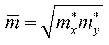
 values are larger than
  for both the electrons and holes of the two monolayers.
|
|
|
C 2D x | C 2D y | E d x | E d y | μ x | μ y | ||
|---|---|---|---|---|---|---|---|---|---|
| Electron | ZrSiSP2 | 1.17 | 5.05 | 189.69 | 189.71 | −5.32 | −3.75 | 49.99 | 23.57 |
| ZrSiSAs2 | 1.36 | 5.93 | 171.45 | 171.46 | −4.90 | −3.45 | 39.33 | 18.19 | |
| Hole | ZrSiSP2 | 1.37 | 1.60 | 189.69 | 189.71 | −7.44 | −7.44 | 36.09 | 30.89 |
| ZrSiSAs2 | 1.41 | 1.43 | 171.45 | 171.46 | −6.91 | −6.91 | 38.15 | 37.62 | |


The elastic modulus C2D can be calculated by using:
 | (6) |
The DP constant Ed is defined by:
 | (7) |
The VBM/CBM positions and the total energy shifting are evaluated along two in-plane directions within the applied strains εuni of −0.4 to 0.4%. By fitting the dependence of band edge energies with strains, the C2D and Ed values can be obtained.51,52 The calculated shifting energies and VBM/CBM positions of the ZrSiSP2 and ZrSiSAs2 monolayers are presented in Fig. 10. We can see that the C2D values are almost the same in the x and y directions, with only slight differences in the C2Dx and C2Dy from 189.69 to 198.71 N m−1 for ZrSiSP2 and 171.45 to 171.46 N m−1 for ZrSiSAs2, respectively. Besides, the positions of band edges are also independent of the two in-plane directions for the two monolayers. Table 2 lists our calculated values of the C2D and Ed. The DP constants of ZrSiSP2 and ZrSiSAs2 in the x and y axes for the electrons are quite anisotropic. From eqn (4), we can attain the μ2D by using the above calculated C2D, m* and Ed values as tabulated in Table 2. The carrier mobilities μx in the x direction of the two studied structures are larger than the carrier mobilities μy in the y direction. This is related to their effective masses, where  is lower than
  . The electron mobility values of ZrSiSP2 are also larger than the electron mobilities of ZrSiSAs2, while the hole mobilities of ZrSiSAs2 are larger than that of ZrSiSP2. The hole mobilities of about 30 cm2 V−1 s−1 of the studied monolayers are larger than the hole mobility values of the recently reported 2D Janus STiSiP2 and STiSiAs2 materials.40 Thus, we can see that the carrier mobilities of ZrSiSP2 and ZrSiSAs2 are anisotropic not only in transport directions but also for the electrons and holes.
 | ||
| Fig. 10 The strain-dependence εunix/y of the total energies and CBM/VBM energies of (a) ZrSiSP2, and (b) ZrSiSAs2. The solid lines present the fitted data. | ||
4 Concluding remarks
Hence, we have designed and studied the crystal lattice as well as the dynamic stability of the ZrSiSZ2 (Z = N, P, As) monolayers using DFT calculations. Except for ZrSiSN2 with the presence of an imaginary frequency in the phonon spectrum, the two ZrSiSP2 and ZrSiSAs2 structures are dynamically stable and have good thermal stability at room temperature and high energetic/mechanical stabilities for the experimental synthesis. We then systematically examine the electronic and transport properties of these stable ZrSiSP2 and ZrSiSAs2 structures. The PBE and HSE06 results demonstrate that the two studied monolayers are in-direct semiconductors with band-gap energies of 1.04 to 1.29 eV for visible light absorption. These moderate band gaps are an advantage for photovoltaic applications of the ZrSiSP2 and ZrSiSAs2 materials. The impacts of external electric fields and applied biaxial strains on the band structures of the monolayers are investigated. It is found that the band-gaps are slightly decreased for a larger E while when the applied εb increases from the compressive to tensile strains, the band-gap energies also increase. For the transport properties, the effective masses and carrier mobilities are calculated based on the DP method. The calculations show that the carrier mobility values in the x direction of the two studied structures are larger than the carrier mobilities in the y direction related to their lower effective masses. The carrier mobilities of the ZrSiSP2 and ZrSiSAs2 monolayers are anisotropic not only in transport directions but also for the electrons and holes. We believe that our study may inspire further investigations and studies to explore more new 2D Janus materials with specific properties for relevant applications.Conflicts of interest
There are no conflicts of interest to declare.Acknowledgements
This research was funded by Hue University under grant no. DHH2023-04-207.References
- K. S. Novoselov, A. K. Geim, S. V. Morozov, D. Jiang, Y. Zhang, S. V. Dubonos, I. V. Grigorieva and A. A. Firsov, Science, 2004, 306, 666 CrossRef CAS PubMed.
- F. Song, L. Bai, A. Moysiadou, S. Lee, C. Hu, L. Liardet and X. Hu, J. Am. Chem. Soc., 2018, 140, 7748–7759 CrossRef CAS PubMed.
- D. Singh, S. K. Gupta, Y. Sonvane and I. Lukačević, J. Mater. Chem. C, 2016, 4, 6386–6390 RSC.
- F. Yang, A. O. Elnabawy, R. Schimmenti, P. Song, J. Wang, Z. Peng, S. Yao, R. Deng, S. Song, Y. Lin, M. Mavrikakis and W. Xu, Nat. Commun., 2020, 11, 1088 CrossRef CAS PubMed.
- J. Pang, A. Bachmatiuk, Y. Yin, B. Trzebicka, L. Zhao, L. Fu, R. G. Mendes, T. Gemming, Z. Liu and M. H. Rummeli, Adv. Energy Mater., 2017, 8, 1702093 CrossRef.
- Y. Gogotsi and B. Anasori, ACS Nano, 2019, 13, 8491–8494 CrossRef CAS PubMed.
- G. Giuffredi, T. Asset, Y. Liu, P. Atanassov and F. D. Fonzo, ACS Mater. Au, 2021, 1, 6–36 CrossRef CAS PubMed.
- Y. Dahiya, M. Hariram, M. Kumar, A. Jain and D. Sarkar, Coord. Chem. Rev., 2022, 451, 214265 CrossRef CAS.
- A. C. Riis-Jensen, T. Deilmann, T. Olsen and K. S. Thygesen, ACS Nano, 2019, 13, 13354–13364 CrossRef CAS PubMed.
- T. Tan, X. Jiang, C. Wang, B. Yao and H. Zhang, Adv. Sci., 2020, 7, 2000058 CrossRef CAS PubMed.
- M. Zhao, Y. Hao, C. Zhang, R. Zhai, B. Liu, W. Liu, C. Wang, S. H. M. Jafri, A. Razaq, R. Papadakis, J. Liu, X. Ye, X. Zheng and H. Li, Crystals, 2022, 12, 1087 CrossRef CAS.
- M. Dragoman, A. Dinescu and D. Dragoman, Phys. Status Solidi A, 2019, 216, 1800724 CrossRef.
- Z. Liu, H. Wang, J. Sun, R. Sun, Z. F. Wang and J. Yang, Nanoscale, 2018, 10, 16169–16177 RSC.
- F. Khan, H. Din, S. Khan, G. Rehman, M. Bilal, C. V. Nguyen, I. Ahmad, L.-Y. Gan and B. Amin, J. Phys. Chem. Solids, 2019, 126, 304–309 CrossRef CAS.
- D. Tyagi, H. Wang, W. Huang, L. Hu, Y. Tang, Z. Guo, Z. Ouyang and H. Zhang, Nanoscale, 2020, 12, 3535–3559 RSC.
- F. R. Fan, R. Wang, H. Zhang and W. Wu, Chem. Soc. Rev., 2021, 50, 10983–11031 RSC.
- Y. Zhu, L. Peng, Z. Fang, C. Yan, X. Zhang and G. Yu, Adv. Mater., 2018, 30, 1706347 CrossRef PubMed.
- L. Zhang, J. Yu, M. Yang, Q. Xie, H. Peng and Z. Liu, Nat. Commun., 2013, 4, 1443 CrossRef PubMed.
- J. Zhang, S. Jia, I. Kholmanov, L. Dong, D. Er, W. Chen, H. Guo, Z. Jin, V. B. Shenoy, L. Shi and J. Lou, ACS Nano, 2017, 11, 8192–8198 CrossRef CAS PubMed.
- Y.-C. Lin, C. Liu, Y. Yu, E. Zarkadoula, M. Yoon, A. A. Puretzky, L. Liang, X. Kong, Y. Gu, A. Strasser, H. M. Meyer, M. Lorenz, M. F. Chisholm, I. N. Ivanov, C. M. Rouleau, G. Duscher, K. Xiao and D. B. Geohegan, ACS Nano, 2020, 14, 3896–3906 CrossRef CAS PubMed.
- H. Yao, C. Zhang, Q. Wang, J. Li, Y. Yu, F. Xu, B. Wang and Y. Wei, Nanomaterials, 2021, 11, 559 CrossRef CAS PubMed.
- X. Liu, H. Zhang, Z. Yang, Z. Zhang, X. Fan and H. Liu, Phys. Lett. A, 2021, 420, 127751 CrossRef CAS.
- Y. Gao, J. Liao, H. Wang, Y. Wu, Y. Li, K. Wang, C. Ma, S. Gong, T. Wang, X. Dong, Z. Jiao and Y. An, Phys. Rev. Appl., 2022, 18, 034033 CrossRef CAS.
- H. Zhong, W. Xiong, P. Lv, J. Yu and S. Yuan, Phys. Rev. B, 2021, 103, 085124 CrossRef CAS.
- W. Zhang, W. Yang, Y. Liu, Z. Liu and F. Zhang, Front. Phys., 2022, 17, 63509 CrossRef.
- N. Mwankemwa, H.-E. Wang, T. Zhu, Q. Fan, F. Zhang and W. Zhang, Results Phys., 2022, 37, 105549 CrossRef.
- Y.-L. Hong, Z. Liu, L. Wang, T. Zhou, W. Ma, C. Xu, S. Feng, L. Chen, M.-L. Chen, D.-M. Sun, X.-Q. Chen, H.-M. Cheng and W. Ren, Science, 2020, 369, 670–674 CrossRef CAS PubMed.
- G. Kresse and J. Furthmüller, Phys. Rev. B: Condens. Matter Mater. Phys., 1996, 54, 11169–11186 CrossRef CAS PubMed.
- G. Kresse and J. Furthmüller, Comput. Mater. Sci., 1996, 6, 15–50 CrossRef CAS.
- A. Togo, L. Chaput and I. Tanaka, Phys. Rev. B: Condens. Matter Mater. Phys., 2015, 91, 094306 CrossRef.
- S. Nosé, J. Chem. Phys., 1984, 81, 511 CrossRef.
- J. P. Perdew, K. Burke and M. Ernzerhof, Phys. Rev. Lett., 1996, 77, 3865 CrossRef CAS PubMed.
- A. H. MacDonald, W. E. Picket and D. D. Koelling, J. Phys. C: Solid State Phys., 1980, 13, 2675 CrossRef CAS.
- J. Heyd, G. E. Scuseria and M. Ernzerhof, J. Chem. Phys., 2003, 118, 8207 CrossRef CAS.
- S. Grimme, J. Antony, S. Ehrlich and H. Krieg, J. Chem. Phys., 2010, 132, 154104 CrossRef PubMed.
- H. J. Monkhorst and J. D. Pack, Phys. Rev. B: Condens. Matter Mater. Phys., 1976, 13, 5188–5192 CrossRef.
- J. Bardeen and W. Shockley, Phys. Rev., 1950, 80, 72 CrossRef CAS.
- S. Haastrup, M. Strange, M. Pandey, T. Deilmann, P. S. Schmidt, N. F. Hinsche, M. N. Gjerding, D. Torelli, P. M. Larsen, A. C. Riis-Jensen, J. Gath, K. W. Jacobsen, J. J. Mortensen, T. Olsen and K. S. Thygesen, 2D Mater., 2018, 5, 042002 CrossRef CAS.
- N. T. Hiep, N. P. Q. Anh, H. V. Phuc, C. Q. Nguyen, N. N. Hieu and V. T. T. Vi, Phys. Chem. Chem. Phys., 2023, 25, 8779–8788 RSC.
- Z. Gao, X. He, W. Li, Y. He and K. Xiong, Dalton Trans., 2023, 52, 8322–8331 RSC.
- K.-A. N. Duerloo, M. T. Ong and E. J. Reed, J. Phys. Chem. Lett., 2012, 3, 2871–2876 CrossRef CAS.
- R. C. Andrew, R. E. Mapasha, A. M. Ukpong and N. Chetty, Phys. Rev. B: Condens. Matter Mater. Phys., 2012, 85, 125428 CrossRef.
- N. T. Hung, A. R. T. Nugraha and R. Saito, J. Phys. D: Appl. Phys., 2018, 51, 075306 CrossRef.
- O. Leenaerts, H. Peelaers, A. D. Hernández-Nieves, B. Partoens and F. M. Peeters, Phys. Rev. B: Condens. Matter Mater. Phys., 2010, 82, 195436 CrossRef.
- Y. Liu, C. Shao, W. Yu, Q. Gui, J. Robertson and Y. Guo, Appl. Phys. Lett., 2022, 121, 244105 CrossRef CAS.
- T. Cheng, H. Lang, Z. Li, Z. Liu and Z. Liu, Phys. Chem. Chem. Phys., 2017, 19, 23942–23950 RSC.
- R. M. Meftakhutdinov and R. T. Sibatov, Nanomaterials, 2022, 12, 3904 CrossRef CAS PubMed.
- A. Politano and G. Chiarello, Nano Res., 2015, 8, 1847–1856 CrossRef CAS.
- J. P. Perdew and M. Levy, Phys. Rev. Lett., 1983, 51, 1884–1887 CrossRef CAS.
- L. Hedin, Phys. Rev., 1965, 139, A796 CrossRef.
- W. Wan, S. Zhao, Y. Ge and Y. Liu, J. Phys.: Condens.Matter., 2019, 31, 435501 CrossRef CAS PubMed.
- S.-D. Guo, W.-Q. Mu, Y.-T. Zhu, R.-Y. Han and W.-C. Ren, J. Mater. Chem. C, 2021, 9, 2464–2473 RSC.
| This journal is © The Royal Society of Chemistry 2023 |