
Enhanced far-field coherent thermal emission using mid-infrared bilayer metasurfaces†
Sichao
Li
 a,
Robert E.
Simpson
b and
Sunmi
Shin
*a
a,
Robert E.
Simpson
b and
Sunmi
Shin
*a
aDepartment of Mechanical Engineering, Collage of Design and Engineering, National University of Singapore, 9 Engineering Drive 1, 117575, Singapore. E-mail: mpeshin@nus.edu.sg
bSchool of Engineering, University of Birmingham, Edgbaston, B15 2TT, UK
First published on 14th July 2023
Abstract
A classical thermal source, such as an incandescent filament, radiates according to Planck's law. The feasibility of super-Planckian radiation has been investigated with sub-wavelength-sized sources in the last decade. In such sources, a crystal-dependent coupling of photons and optical phonons is possible at thermal energies corresponding to that at room temperature. This interaction can be used to tailor the far-field thermal emission in a coherent manner; however, understanding heat transfer during this process is still nascent. Here, we used a novel measurement platform to quantify thermal signals in a Ge2Sb2Te5/SiO2 nanoribbon structure. We were able to separate and quantify the radiated and conducted heat transfer mechanisms. The thermal emission from the Ge2Sb2Te5/SiO2 nanoribbons was enhanced by 3.5× compared to that of a bare SiO2 nanoribbon. Our model revealed that this enhancement was directly due to polaritonic heat transfer, which was possible due to the large and lossless dielectric permittivity of Ge2Sb2Te5 at mid-IR frequencies. This study directly probes the far-field emission with a thermal gradient stimulated by Joule heating in temperature ranges from 100 to 400 K, which bridges the gap between mid-IR optics and thermal engineering.
 Sunmi Shin | Sunmi Shin joined NUS as an assistant professor and a research assistant professor in 2019 and 2018, respectively. Prior to joining NUS, she received her Ph.D. in Materials Science and Engineering from UC San Diego in 2019, and her B.S. and M.S. degrees in Chemical Engineering from Hanyang University in 2011 and 2014, respectively. She specializes in an experimental investigation on fundamental nanoscale heat transport for thermal management and development of personalized thermo-regulators and energy harvesting devices using thermoelectric energy conversion. Her research interests include a multidisciplinary approach for efficient and active heat control across mechanical engineering and materials science. |
Introduction
Thermal emission is determined by Planck's law and is generally considered fixed by the material properties. However, many recent studies have tuned the thermal radiation spectrum using photonic crystals,1–8 cavities9–11 and gratings.12–17 The technique essentially relies on nanostructuring the material's surface to modify its optical absorption. Kirchhoff's law states that the equilibrium thermal emission spectrum corresponds to the absorptance of the material; hence the radiation spectrum can be modified. The spectral and temporal coherency in the emission spectrum has been studied by adopting metasurfaces where the mid-IR optical property is closely correlated with the crystal lattice, mainly optical phonons. The dominant thermal wavelength at finite temperature is determined by Wien's law (λT = b/T), where b is Wien's displacement constant and T is the temperature. Hence, this implies that there is a blurred boundary between two distinct disciplines, optics and thermal engineering. However, it is still questionable whether one can simply treat thermal sources as alternatives to mid-IR optical sources. Clarifying this knowledge gap is important for utilizing the radiative heat flux that is driven by a temperature gradient. The possibility of super-Planckian thermal emission is controversial. Golyk et al.19 reported suppressed thermal emission from structures with dimensions smaller than the skin depth. Contrarily, Biehs and Ben-Abdallah20 revealed that there is no theoretical upper limit to thermal emission from finite-sized systems in the far field. While many theoretical studies have recently predicted non-Planckian thermal emission, it has not yet been confirmed experimentally.There are two perspectives involved to understand the super-Planckian behavior: (1) enhanced radiation beyond the blackbody limit and (2) radiation distribution deviating from Planck's law. The term super-Planckian thermal emission has been introduced to describe the enhanced thermal radiation beyond the blackbody in near-field radiation across the nano-gaps between two objects.21 Recent experimental and computational developments to study far-field radiation from a nano-object have opened the era to revisit the super-Planckian thermal emission in the far-field.22 The emissivity and absorptivity of an object are equal at the equilibrium imposed by the laws of thermodynamics. As such, it has been admitted that the far-field radiation cannot be beyond the blackbody limit, and therefore, the upper limit of radiation from an infinite planar medium is bound by the blackbody emission. Similarly, the implementation of nanostructured arrays in a large unit rarely leads to enhanced thermal emission. The beauty of investigating super-Planckian thermal emission origins from the fact that the emissivity can be beyond 1 with no upper limit in the modulated spectral and/or spatial range.23 However, the potential of the upper limit by enlarging the absorption cross-sectional area has not been clarified yet. Our study employs a state-of-the-art thermometry platform to quantify the emissivity of a single object by sensitively detecting the temperature rises at equilibrium and investigates enhanced far-field emission in nanostructures.
Experimentally studying non-Planckian thermal emission is challenging due to the low emission powers of an object with sub-wavelength dimensions. Indeed, very few experimental investigations have been attempted.22 Thermal emission control by photonic structures has mainly been studied using metals at high temperatures, typically around 1000 K.24 However, directly and accurately probing powers down to the nW level without significantly heating the structure makes measuring sub-wavelength emitters at room temperature exceedingly difficult. To achieve measurable emission, it is important to access a wide range of photon density of states, which can increase the radiation rate to the far field. One technique to do this involves exploiting internal reflection by introducing evanescent waves confined on the emitter's surface. Remarkably, surface phonon polaritons (SPhPs) can confine mid-IR electromagnetic waves on the surface of polar dielectrics.22,25–28 The effect originates from coupling photons and optical phonons. It occurs within the so-called Reststrahlen band where transverse optical phonons resonate at frequencies (ωTO) similar to longitudinal optical phonons (ωLO). These confined phonon–photon coupled surface waves have enhanced near-field thermal radiation, which can even exceed the blackbody limits.27–29 Our previous study reported 8.5× higher emissivity of SiO2 nanoribbons compared to a thin film with an otherwise similar structure. The enhancement stemmed from a strong resonance at thermal wavelengths.18 Furthermore, controlling dispersion via Au-dot/SiO2 metasurfaces enabled the enhancement of thermal emission by broadening the effective energy range to support SPhPs.30
Herein, we study the influence of a thin polar dielectric layer on far-field coherent emission. Recent studies using different optical experiments on nanophotonic bilayer systems have shown enhanced radiation intensities in the mid-infrared regime.8,31–35 However, it is noteworthy that direct thermal observations have been seldom investigated due to the lack of experimental platforms to study low-energy and low-intensity far-field radiation. We customized nanostructures to emit radiation that can be distinguished from the convection and conduction heat transfer mechanisms. The specimens were integrated into a sensitive thermometer to probe the emissivity. Our novel measurement platform allowed us to quantify thermal signals and to exploit mid-infrared photonic metasurfaces to modulate heat transfer. We compared the emissivity of a bare SiO2 nanoribbon with that of Ge2Sb2Te5 (GST)/SiO2 bilayer nanoribbons. The additional thin layer of a dielectric film with a large but lossless refractive index induced highly confined evanescent waves at the interface between Ge2Sb2Te5 and SiO2, and the tailored energy dispersion of the bilayer metasurfaces could enhance the thermal emission.
We designed bilayer nanoribbon structures to enlarge the surface-to-volume ratios and concomitantly make the radiative heat transfer dominant. A state-of-the-art methodology, which uses a sensitive thermometry platform, was adopted to probe the emissivity of a single nanostructure. The technique involved fabricating finite-sized emitters integrated into a suspended micro-thermometer. The bilayer nanostructure consisted of a thin layer of amorphous-phase Ge2Sb2Te5 (a-GST) on top of an SiO2 nanoribbon. The high contrast in the permittivity (ε = ε′ + ε′′i) of the two different layers produced an asymmetric electric field distribution across the top and bottom surfaces as well as at the interface between them. Previously, we used a micro-thermometry platform to directly measure the far-field emissivity of individual nano-objects.18,30,36 Here, we demonstrate the enhanced emissivity using the Ge2Sb2Te5/SiO2 bilayer and report the enhanced emissivity of over 3.5 times that of the bare SiO2 emitter.
Methods
Design of suspended nanoribbon samples
We designed a nano-specimen to reveal the dominant heat transfer by coherent thermal emissions. First, we considered that thermal transport by conduction (G) is either comparable with or insignificant compared to that by radiation. As shown in Fig. 1(e), the contributions by conduction (Gcond = κAc/L, where κ, Ac and L represent the thermal conductivity, the cross-sectional area and the length of an object) and radiation (Grad = 4εσAT3, where ε, A and T represent the emissivity, the surface area and the temperature of the object and σ is the Stefan–Boltzmann constant) can be distinguished by varying the length of the nanostructures. In general, the higher the aspect ratio of the surface to volume of the emitter, the more significant the heat transfer by radiation. Furthermore, incoherent thermal emission from the solid volume was suppressed by limiting one of the structure's dimensions to be smaller than the skin depth in the mid-IR regime.19 In this study, we designed our structures to be much thinner (e.g. 100 nm thickness) than the skin depth of ∼1 μm in SiO2 to suppress the incoherent thermal emission from the volume, rather we investigate the surface effect to study the enhanced coherent thermal emission by SPhPs. Also, we fixed the width of 5 μm and varied the length from 70 to 800 μm. Unlike most crystalline solids, amorphous SiO2 rarely presents size-dependent thermal conductivity due to the short mean free path of <10 s nm.37,38 This fact was used to calibrate our measurement system, as well as to observe the distinct change of the apparent thermal conductivity (κapp), which is influenced by radiation when the lattice thermal conductivity is maintained. Furthermore, we introduced a Ge2Sb2Te5 layer on top of the SiO2 nanostructure, which was sufficiently thin to make a negligible contribution to the total heat transported by conduction. | ||
| Fig. 1 Schematics of the electric field distribution of (a) confined SPhP mode generated by an amorphous SiO2 nanoribbon structure and (b) ultra-confined SPhP enabled by a Ge2Sb2Te5 (GST) thin layer covered SiO2 nanoribbon at both x–y plane views. The schematics are mimicked from the numerical electrical field distribution for (c) bare SiO2 and (d) Ge2Sb2Te5/SiO2, respectively. (e) Plots of calculated thermal conduction due to phonon conduction and radiation heat loss as a function of the sample length. Input emissivity value is 0.17, which corresponds to the emissivity we obtained from the Ge2Sb2Te5/SiO2 sample at room temperature. (f) Schematic of our sample, with a continuous GST thin layer deposited on a suspended SiO2 nanoribbon. A zoomed-in schematic of the joint of the sample and beams highlights that, to avoid electrical leakage from the Pt to GST material, we performed pre-etching of the GST layer for the electrode pattern areas to make sure the disconnection between Pt and GST. (g) SEM images of our suspended Ge2Sb2Te5/SiO2 nanoribbon sample with (h) a zoom-in image of the sample and beam structure. The width of the nanoribbon was designed as 5 μm, which is the half of the thermal wavelength (10 μm at room temperature) to further enhance the coherent thermal emission by SPhPs. The final sample width is 5.42 μm (with ∼0.3 μm error range for each sample). | ||
Fig. 1(e) shows the estimated thermal conductance by conduction and radiation. In the analytical model, a 5 μm wide and 130 nm thick nanoribbon (NR) was considered with emissivity of 0.17. These values are the designed and measured values from the Ge2Sb2Te5/SiO2 samples, which we will introduce later. Heat transfer by radiation dominates for NRs longer than ∼800 μm. This critical length decreases at higher emissivity and at higher operating temperatures. Thus, for this study we fabricated NRs with different lengths varying up to 800 μm.
The Ge2Sb2Te5/SiO2 NRs were integrated into our thermometry micro-devices as shown in Fig. 1(f), where the specimen is located across two suspended metal beams. Notably, the sample specimen and beams were fabricated based on a single unit of SiO2, which gives negligible contact thermal resistance from the beam to heat channel. Generally, the κapp of NRs were measured by applying AC-modulated heating and detecting the temperature rises at both beams. Importantly, the AC-modulated heating method allowed us to systematically control thermal penetration by varying the heating frequency. Further analysis in the frequency domain could differentiate the influence of the conduction and radiation heat transfer mechanisms. We compared the thermal emissions of bare SiO2 and bilayer Ge2Sb2Te5/SiO2 NRs. Note that our experiments were entirely thermal based. They rely on directly probing the far-field emission with a thermal gradient stimulated by Joule heating, which can be different from the optical methods using monochromatic incident waves.
Sample fabrication
We first sputtered a 30 nm thick amorphous Ge2Sb2Te5 layer on a 100 nm thermal oxide Si wafer (Fig. S1†). As shown in the inset of Fig. 1(f), the Ge2Sb2Te5 area on the sample specimen was set slightly smaller than that of the SiO2 NR. Next, a 4 nm thick Ti layer and a 76 nm Pt layer were deposited by e-beam evaporation. Note that the resistivity of Ge2Sb2Te5 abruptly switches from 104 to 101 ohm m−1 at its amorphous to face centered cubic (FCC) phase transition temperature;39 therefore the Ge2Sb2Te5 layer was patterned and pre-etched by reactive ion etching (RIE) to avoid direct contact with the Ti/Pt metal layer. Subsequent patterning and etching were used to define the suspended area covering the beams and the sample bridge. Lastly, the Si substrate was etched by isotropic XeF2 etching to make the patterned Ge2Sb2Te5/SiO2 bilayer suspended.AC-modulated thermometry
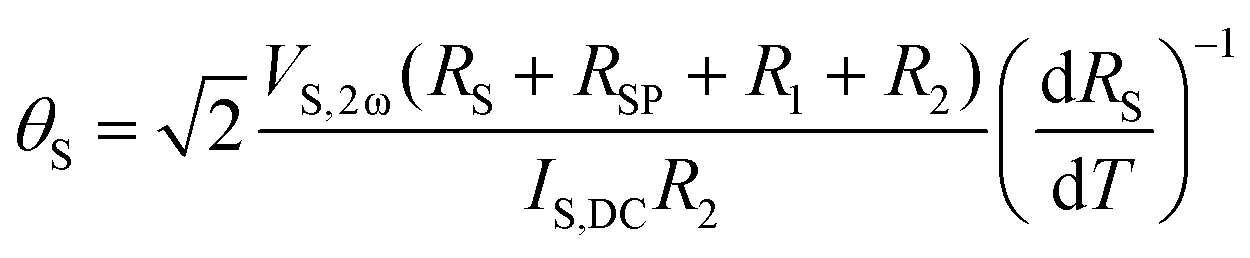
We employed an AC-modulated thermometry platform (illustrated in Fig. 3(a)) with a measurement resolution of <1 nW K−1 to accurately detect temperature rises in the nanoribbons.36 The temperature rise at the heating side (θH) with AC joule heating at 1ω angular frequency can be detected by the 3rd harmonic voltage signal (VH,3ω), which is the well-known 3ω method.40 At the sensing side, the temperature rise (θS) is measured by detecting the 2nd harmonic voltage signal (VS,2ω) with direct current (DC) applied. To further increase the sensitivity, a Wheatstone bridge circuit was applied at the sensing side. The measurement was conducted in a high vacuum (<10−6 Torr); thus, the convective heat transfer was negligible in our experiment. The theoretical temperature distribution for samples with different lengths can be seen in Fig. S2.† When there is no significant heat loss (short samples), the temperature distribution along the sample is dominated by phonon conduction, which led to the observed linear trend, as described by Fourier's law (blue line). Nevertheless, when radiative heat loss starts to dominate in the longer samples, the radiative heat transfer coefficient (h = 4σεT3) needs to be considered, which results in a lower temperature rise along the sample (red line). The exact temperature of the NR can be determined by the voltage signal as follows: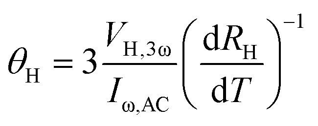 | (1) |
 | (2) |
Dielectric constant of Ge2Sb2Te5 in the mid-IR regime
To determine the dielectric constant of Ge2Sb2Te5, the Drude and modified Tauc–Lorentz models were used, following the previous study by Chew et al.41 The imaginary part of the permittivity was fitted using eqn (3). | (3) |
The Kramers–Kronig relationship was used to calculate the real part of the dielectric constant as:
 | (4) |
 is the principal value of the integral. ATL is a constant calculated by the Tauc coefficient and the strength of the Lorentzian peak. C is a constant broadening term. All fitted parameters from reported experimental values are summarized in Table S1.†
In general, amorphous Ge2Sb2Te5 possesses an almost zero imaginary part of the permittivity in the mid-IR regime and a constant real part of 13.8 (Fig. 2(b)). The lossless optical property within the Reststrahlen band of SiO2 can be utilized to realize highly confined modes within the Ge2Sb2Te5/SiO2 bilayer system. The obtained permittivity was used to calculate the energy dispersion relationship in the Ge2Sb2Te5/SiO2 bilayer NRs.
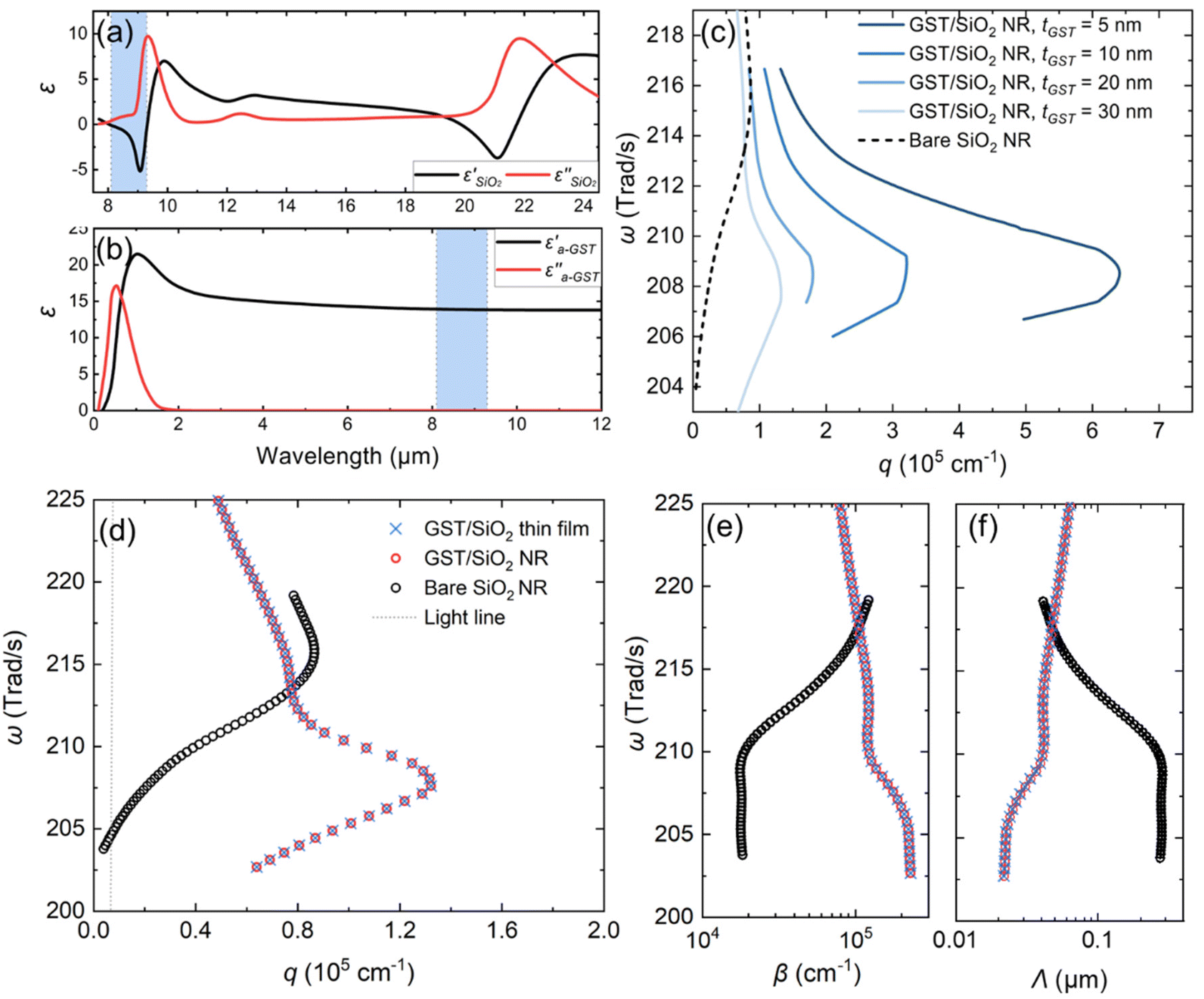 | ||
| Fig. 2 Wavelength-dependent dielectric constants of (a) SiO2 and (b) a-GST we used for our calculations, respectively. Shadowed areas are the Reststrahlen band regime for amorphous SiO2, where SiO2 shows a negative dielectric constant while a-GST shows constant permittivity. (c) Energy dispersions of various thicknesses (5 to 30 nm) of a-GST covered SiO2 nanoribbons calculated by our numerical modelling. (d) Numerical results of energy dispersion for a 5 μm width bare SiO2 NR, Ge2Sb2Te5/SiO2 NRs, and a Ge2Sb2Te5/SiO2 thin film. The gray dotted line represents the light line. It can be clearly seen that the energy dispersion of fundamental modes in a-GST/SiO2 NRs are superimposed with their thin film counterparts. Comparison of the imaginary part of the wavevector, β (e), and the propagation length, Λ (f), between Ge2Sb2Te5/SiO2 and bare SiO2 emitters. It shows a 30 nm additional GST layer, and Λ can be further squeezed down to the 10−2 μm level, which can be 10 times smaller than the bare SiO2 in our energy range of interest. The results can further support that additional 30 nm a-GST indeed enhances the confinement of SPhPs compared with bare SiO2. | ||
Results and discussion
Modelling of ultra-confined SPhPs by the Ge2Sb2Te5 /SiO2 bilayer
We modelled the dispersion relationship of the Ge2Sb2Te5/SiO2 bilayer and compared it with that of bare SiO2. Full-wave numerical simulations using the finite-element method in the frequency domain (COMSOL Multiphysics) were performed to study the confined surface modes supported by the bilayer structures. A bare SiO2 nanoribbon itself can support SPhPs as shown in Fig. 1(a), but when a thin Ge2Sb2Te5 layer is added on top of the SiO2 layers, it supports further confined SPhPs within the Reststrahlen band.The thickness of the Ge2Sb2Te5 layer was systematically varied to find the optimal thickness to maximize thermal emission. The dispersion energies for Ge2Sb2Te5 thicknesses from 5 nm to 30 nm on a 100 nm thick and 5 μm wide SiO2 nanoribbon were studied. As shown in Fig. 1(c), adding the thin Ge2Sb2Te5 layer increases the allowed wavevectors compared to bare SiO2 NRs. This effect is consistent with that predicted in a study by Li et al.4 Approximately 30× higher wavevectors (q) were achieved by adding a 5 nm thick Ge2Sb2Te5 layer. Moreover, the peak q wavevector is red-shifted in the bilayer system, which implies the coupling of the dielectric layer and SiO2. Similarly, we also analyzed the energy dispersion of the Ge2Sb2Te5/SiO2 bilayer after crystallizing Ge2Sb2Te5 into its FCC phase, see the ESI (Fig. S3†). However, the negligible imaginary component of the amorphous Ge2Sb2Te5 dielectric function makes it more suitable for studying the influence of SPhPs.
We designed the bilayer specimens to behave similarly to thin films to maximize the influence of surface phonon polaritons by multilayers (including the top and bottom surfaces as well as the interface), rather than the side walls or edges in the nanostructured specimen. At the same time, we optimized the width of nanoribbons to be small to suppress the conductance by heat conduction while maintaining a relatively large surface area to effectively enlarge the conductance by radiation. As a result, we employed ∼5 μm width and confirmed that the energy dispersion of bilayer specimens with 5 μm behaves the same as that of one of thin films in Fig. 2(d). This result means that the surface waves are confined at the interfaces between the SiO2 and Ge2Sb2Te5 layers, rather than the side walls or edges. Also, the imaginary part of the wavevector (β) and the propagation length (Λ) in the 5 μm-wide NR are well overlapped with the ones for thin films. It was clearly seen that the addition of 30 nm thick Ge2Sb2Te5 on SiO2 results in highly confined modes with high q, and correspondingly, more energy losses with the short Λ. This indicates an efficient energy absorption (= emission) of mid-IR waves from the thin structures.
Enhanced far-field emission from GST/SiO2 nanoribbons
We first conducted the thermal conductivity measurement at various temperatures ranging from 100 to 400 K. It is noteworthy that the temperature-controlled measurement allows us to differentiate the radiative and conductive heat transfers. At higher temperatures, radiative heat transfer is dominant. Similarly, we also varied the surface area of specimens by adopting a wide range of lengths from 70 to 800 μm. Larger surface areas should increase thermal emission. Empty devices, without NRs, were also measured to compare with the NR samples such that the effect of NRs can be determined. The temperature rises were measured for different heating powers in the empty device in both heating (θH) and sensing (θS) beams, as shown in Fig. 3(b). There is a negligible temperature rise at the sensing beam in response to heating the heater. This measurement directly confirms that there is insignificant background far-field thermal emission between the long metal beams in our device. Thus, we can infer that any radiative heat transfer must be due to the surface of nanoribbons. | ||
| Fig. 3 (a) Illustration of an AC-modulated thermometry platform with a cryostat vacuum chamber. Our thermal measurement was conducted at a high vacuum level (<10−6 Torr) to suppress the convection with the surrounding. Three additional radiative shields were applied to avoid radiative heat loss to the ambient. (b) Metal beam emission checked by comparing the input power-dependent sensing side temperature rise for a structure with and without an NR sample. No heating power-dependent temperature rise at the sensing side is observed with the empty beam, which indicates that the direct beam emission (background) can be negligible for our sensitive measurement platform, and all the sensing side signals originate from our NR sample. (c) Plot of temperature-dependent apparent thermal conductivity of bare SiO2, as well as Ge2Sb2Te5/SiO2 NRs with the same width design (5 μm) but various lengths (70, 400 and 800 μm). Our bulk thermal conductivity measurement data fitted well with the reference,18 the shadowed areas represent the range for fitted emissivity values. The difference between 70 μm sample groups comes from the intrinsic bulk conductivity between bare SiO2 and 30 nm a-GST + 100 nm SiO2 because for the 70 μm length the thermal emission has not become dominate due to its short length. The large error bars of long specimens at high temperature are due to the larger systematic errors as we discussed in ESI Note 5.† (d) Plot of the frequency-dependent temperature rise ratio between sensing and heating sides with experimental data (diamond marks) and fitting curves, the shadowed area represents the radiative heat loss. The inset plot shows the frequency-dependent thermal penetration depth (Lp). With increasing frequency, Lp decreases, which can lead to a dynamic change of the effective length for emission, thus can provide the fitting process for the experimental data and calculated curves. | ||
Fig. 3(c) compares the κapp value of bilayer Ge2Sb2Te5/SiO2 NRs with that of bare SiO2 NRs. The κapp value is influenced by both radiation and conduction. Short SiO2 NRs with 20 and 70 μm show almost bulk-like thermal conductivity over the wide range of temperatures due to insignificant radiative heat loss on the surface. This clearly indicates that nano-emitters need to be designed with high surface-to-volume ratios to detect thermal emission. However, the aspect ratio required increases with the thermal conductivity of the solids, and therefore a much longer and thinner suspended nanostructure need to be fabricated, which is technically more challenging. In our experiment, we chose SiO2 as a polar dielectric with a low thermal conductivity of ∼1.4 W m−1 K−1 (cf., Si3N4 with 9 W m−1 K−1,43 SiC with 490 W m−1 K−1![[thin space (1/6-em)]](https://www.rsc.org/images/entities/char_2009.gif) 44 and hBN with 751 W m−1 K−145). Also, importantly, amorphous SiO2 should not exhibit size-dependent thermal conductivity for the dimensions of our samples, which are down to 100 nm owing to their short phonon mean free paths.37,38 This design allows us to calibrate our measurement system and quantify the contribution of heat conduction for different samples. The 30 nm thin layer of Ge2Sb2Te5 on top of SiO2 has a lower intrinsic thermal conductivity (below 0.5 W m−1 K−1)46 than the 100 nm thick layer of SiO2 (1.4 W m−1 K−1) at 300 K, which matches with our fitted effective thermal conductivity κfit in Fig. 4(a).
44 and hBN with 751 W m−1 K−145). Also, importantly, amorphous SiO2 should not exhibit size-dependent thermal conductivity for the dimensions of our samples, which are down to 100 nm owing to their short phonon mean free paths.37,38 This design allows us to calibrate our measurement system and quantify the contribution of heat conduction for different samples. The 30 nm thin layer of Ge2Sb2Te5 on top of SiO2 has a lower intrinsic thermal conductivity (below 0.5 W m−1 K−1)46 than the 100 nm thick layer of SiO2 (1.4 W m−1 K−1) at 300 K, which matches with our fitted effective thermal conductivity κfit in Fig. 4(a).
 | ||
| Fig. 4 Plot of temperature dependent (a) κfit and (b) absolute emissivity values for both bare SiO2 and GST/SiO2 NRs. The κfit values are obtained during the emissivity extraction. The κfit value can be close to the κapp value of 70 μm GST/SiO2, deviation between bare SiO2 and GST/SiO2 starts at 300 K due to the intrinsic bulk thermal conductivity difference from amorphous Ge2Sb2Te5 to SiO2. | ||
The thermal emission is greater for emitters with a larger surface. As shown in Fig. 3(c), the κapp value starts deviating from the bulk thermal conductivity of SiO2 for the 400 μm and 800 μm long specimens. One can see that the κapp value dramatically decreases with increasing nanoribbon length; indicating that the radiative heat loss has been enhanced for the larger surface areas. By comparing the κapp values of bare SiO2 and Ge2Sb2Te5/SiO2, we quantified the enhanced thermal emission for the bilayer nanoribbons. In Fig. 3(c), the colored area presents the predicted κapp determined by the emissivity, which ranges from 0.15 to 0.25 (0.07 to 0.1) for Ge2Sb2Te5/SiO2 (bare SiO2). At low temperatures, the emitting power is relatively small, and becomes insignificant compared to the thermal conductance in the solid volume. Thus, the κapp values of most samples are similar to the thermal conductivity of bulk SiO2. Larger κapp deviations were observed at higher temperatures. Note that for all the Ge2Sb2Te5/SiO2 samples we controlled the ambient temperature below 400 K, which is well below the amorphous—FCC phase transition temperature (∼420 K). Hence, the amorphous phase of Ge2Sb2Te5 was retained throughout the experiment.
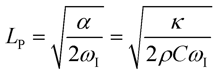
To extract the thermal emissivity of the NRs, we analyzed the temperature rise at different heating frequencies. Effectively, this experiment controls the thermal penetration depth (Lp). In our thermometry platform the suspended emitter is connected to the heating metal beam, and this generates a heat flux parallel to the sample length and thus 1D heat transfer can be considered. The frequency-dependent Lp can be expressed by eqn (5):
 | (5) |
 | (6) |
 | (7) |
 | (8) |
In the low frequency regime, Lp becomes much longer than the length of samples, where the κapp value was determined. The κapp value is influenced by both conduction and radiation. By fitting the measured overall frequency-dependent temperature rises with the modelled ones, we separated the influence of the two different heat transfer mechanisms. In Fig. 3(d), the colored area represents the radiative heat loss carried by SPhPs. By applying the κfit value and considering the radiative heat loss for an emissivity of 0.23, the modelling data (red solid line) can fully fit with our experimental data (black diamonds), as plotted in Fig. 4(a). This result suggests that the emissivity value of our current NR sample is exactly 0.23. These emissivity and thermal conductivity (κfit) values were extracted. This observed value for κfit is almost identical toκbulk, as shown in Fig. 4(a).
In Fig. 4(b), we repeated the analysis to measure the emissivity of specimens at various temperatures and observed that higher values of emissivity are present at lower temperatures for both sample groups (e.g., SiO2 and Ge2Sb2Te5/SiO2 NRs). This trend is explained by changes in the optical permittivity of SiO2, which is a major contributor to determine the radiative properties in the mid-IR regime. Specifically, as the temperature decreases, the lifetime of optical phonons is expected to increase, leading to a smaller damping term in the dielectric function.47,48 This results in a stronger and more coherent thermal emission, which is consistent with the observation of enhanced far-field radiation by Thompson et al.22 as we discussed in ESI Note 6.† Additionally, we compared the emissivities of bare SiO2 and bilayer Ge2Sb2Te5/SiO2 emitters and found that the bilayer metasurfaces could achieve a higher emissivity of up to 0.3. This value corresponds to an emissivity enhancement of up to 3.5× greater than that of the bare SiO2 at 100 K. Numerical modelling of the normalized spectral absorption cross-sectional area of a 5 μm wide Ge2Sb2Te5/SiO2 nanoribbon (σabs/σgeom) is shown in ESI Note 7 (Fig. S5†), indicating that peak emissivity enhancement occurs at the resonant frequencies (ωLO and ωTO) of SPhPs.
Electromagnetic field intensity distribution
We conducted a detailed analysis of the electric field intensity for SiO2 NRs with and without a 30 nm thick Ge2Sb2Te5 layer, as depicted in Fig. 5(a) and (b), respectively. We selected wavelengths near the peak of q in the energy dispersion, which ranged from 8.7 μm to 9.1 μm, and compared the normalized electric field intensity distribution over the thickness of the nanoribbon (y-axis). The SiO2 nanoribbon without the Ge2Sb2Te5 layer exhibits symmetric peak intensities at the top and bottom surfaces. On the other hand, the Ge2Sb2Te5/SIO2 bilayer nanoribbon, with three interfaces, displays asymmetric peaks, where stronger energy confinement is observed at the interface between Ge2Sb2Te5 and SiO2. This characteristic indicates that energy is highly confined within the newly introduced interfaces of the layers that have dissimilar permittivity.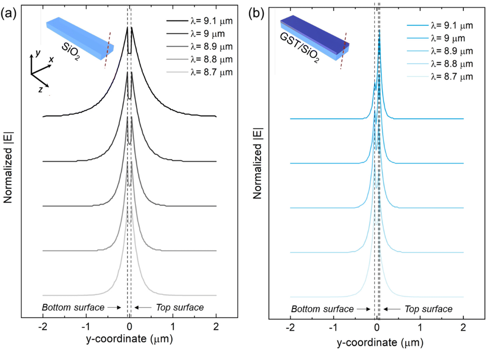 | ||
| Fig. 5 Plot of the electrical field intensity of (a) bare SiO2 and (b) Ge2Sb2Te5/SiO2 NRs with 10 nm thickness a-GST at wavelengths of 8.7–9.1 um (the highest confinement points in the Ge2Sb2Te5/SiO2 system). The electrical field intensity is normalized at the same peak height. The bare SiO2 system has a minor gradual and symmetrical intensity change while the peak electrical field location of Ge2Sb2Te5/SiO2 is changed from the SiO2 bottom surface to the interface between GST and SiO2 which also shows a significant intensity change. | ||
Conclusions
We studied the enhanced far-field thermal emission from mid-IR bilayer nanostructures. We designed bilayer nanoribbon structures that enhance the radiative heat transfer to the point that it dominates over other heat transfer mechanisms. This enhancement enabled us to detect the emissivity of individual nanoribbon structures by making meticulous measurements of the apparent thermal conductivity. The emitter was integrated into a sensitive thermometry platform, and we performed temperature- and frequency-dependent measurements to separate the radiative and conductive heat transfer mechanisms. The separation enables us to evaluate the emissivity and thermal conductivity of specimens simultaneously. This direct measurement of heat transfer revealed that adding a thin high refractive index layer, Ge2Sb2Te5, to the nanoribbon could enhance radiative heat transfer by 3.5×. Our analytical and numerical modeling showed that the electric field is highly confined at the interface of Ge2Sb2Te5 and SiO2, which leads to the observed enhanced radiative emission in the far field. The results show strong and direct experimental evidence for non-Planckian mid-IR thermal emissions at low temperatures. This experimental verification was only possible due to our sensitive platform for separating conductive and radiative heat transfers in nanodevices.Data availability
The data that support the findings of this study are available from the corresponding author on reasonable request.Author contributions
S. L. and S. S. devised the experimental designs. S. L. and R. S. prepared samples. S. L. conducted the thermal measurement and numerical modeling. All authors discussed the results and wrote the manuscript.Conflicts of interest
There are no conflicts to declare.Acknowledgements
The authors acknowledge Prof. Renkun Chen and Yu Pei (UC San Diego) for their insightful comments and valuable assistance on the XeF2 etching process for isotropic Si etching. We acknowledge support from Singapore ministry of education academic research fund tier 1 (A-0009121-01-00 and A-0009061-01-00).References
- V. W. Brar, M. S. Jang, M. Sherrott, S. Kim, J. J. Lopez, L. B. Kim, M. Choi and H. Atwater, Nano Lett., 2014, 14, 3876–3880 CrossRef CAS PubMed.
- M. Liu, X. Yin, E. Ulin-Avila, B. Geng, T. Zentgraf, L. Ju, F. Wang and X. Zhang, Nature, 2011, 474, 64–67 CrossRef CAS PubMed.
- B. Gholipour, J. Zhang, K. F. MacDonald, D. W. Hewak and N. I. Zheludev, Adv. Mater., 2013, 25, 3050–3054 CrossRef CAS PubMed.
- P. Li, X. Yang, T. W. Maß, J. Hanss, M. Lewin, A.-K. U. Michel, M. Wuttig and T. Taubner, Nat. Mater., 2016, 15, 870–875 CrossRef CAS PubMed.
- N. C. Passler, C. R. Gubbin, T. G. Folland, I. Razdolski, D. S. Katzer, D. F. Storm, M. Wolf, S. De Liberato, J. D. Caldwell and A. Paarmann, Nano Lett., 2018, 18, 4285–4292 CrossRef CAS PubMed.
- M. I. Stockman, Nano Lett., 2006, 6, 2604–2608 CrossRef CAS PubMed.
- S.-Y. Lin, M.-L. Hsieh, S. John, B. Frey, J. A. Bur, T.-S. Luk, X. Wang and S. Narayanan, Sci. Rep., 2020, 10, 1–7 CrossRef PubMed.
- A. M. Dubrovkin, B. Qiang, H. N. Krishnamoorthy, N. I. Zheludev and Q. J. Wang, Nat. Commun., 2018, 9, 1–6 CrossRef CAS PubMed.
- T. Taubner, D. Korobkin, Y. Urzhumov, G. Shvets and R. Hillenbrand, Science, 2006, 313, 1595–1595 CrossRef CAS PubMed.
- A. Seif, W. DeGottardi, K. Esfarjani and M. Hafezi, Nat. Commun., 2018, 9, 1–8 CrossRef CAS PubMed.
- O. Florez, G. Arregui, M. Albrechtsen, R. C. Ng, J. Gomis-Bresco, S. Stobbe, C. M. Sotomayor-Torres and P. D. García, Nat. Nanotechnol., 2022, 17, 947–951 CrossRef CAS PubMed.
- J.-J. Greffet, R. Carminati, K. Joulain, J.-P. Mulet, S. Mainguy and Y. Chen, Nature, 2002, 416, 61–64 CrossRef CAS PubMed.
- D. G. Baranov, Y. Xiao, I. A. Nechepurenko, A. Krasnok, A. Alù and M. A. Kats, Nat. Mater., 2019, 18, 920–930 CrossRef CAS PubMed.
- H. Salihoglu, Z. Li and S. Shen, Appl. Phys. Lett., 2022, 121, 241701 CrossRef CAS.
- C. Blanchard, L. Wojszvzyk, C. Jamois, J.-L. Leclercq, C. Chevalier, L. Ferrier, P. Viktorovitch, I. Moldovan-Doyen, F. Marquier, J.-J. Greffet and X. Letartre, Opt. Mater. Express, 2022, 12, 1–12 CrossRef CAS.
- H. Zhang, B. Abhiraman, Q. Zhang, J. Miao, K. Jo, S. Roccasecca, M. W. Knight, A. R. Davoyan and D. Jariwala, Nat. Commun., 2020, 11, 1–9 CrossRef PubMed.
- G. Lu, C. R. Gubbin, J. R. Nolen, T. Folland, M. J. Tadjer, S. De Liberato and J. D. Caldwell, Nano Lett., 2021, 21, 1831–1838 CrossRef CAS PubMed.
- S. Shin, M. Elzouka, R. Prasher and R. Chen, Nat. Commun., 2019, 10, 1377 CrossRef PubMed.
- V. A. Golyk, M. Krüger and M. Kardar, Phys. Rev. E: Stat., Nonlinear, Soft Matter Phys., 2012, 85, 046603 CrossRef PubMed.
- S.-A. Biehs and P. Ben-Abdallah, Phys. Rev. B, 2016, 93, 165405 CrossRef.
- B. Song, D. Thompson, A. Fiorino, Y. Ganjeh, P. Reddy and E. Meyhofer, Nat. Nanotechnol., 2016, 11, 509–514 CrossRef CAS PubMed.
- D. Thompson, L. Zhu, R. Mittapally, S. Sadat, Z. Xing, P. McArdle, M. M. Qazilbash, P. Reddy and E. Meyhofer, Nature, 2018, 561, 216–221 CrossRef CAS PubMed.
- Y. Xiao, M. Sheldon and M. A. Kats, Nat. Photonics, 2022, 16, 397–401 CrossRef CAS.
- S.-Y. Lin, J. Moreno and J. Fleming, Appl. Phys. Lett., 2003, 83, 380–382 CrossRef CAS.
- C. Lucchesi, R. Vaillon and P.-O. Chapuis, Nanoscale Horiz., 2021, 6, 201–208 RSC.
- K. Joulain, R. Carminati, J.-P. Mulet and J.-J. Greffet, Phys. Rev. B: Condens. Matter Mater. Phys., 2003, 68, 245405 CrossRef.
- J. Yang, W. Du, Y. Su, Y. Fu, S. Gong, S. He and Y. Ma, Nat. Commun., 2018, 9, 1–10 CrossRef PubMed.
- K. Shi, Z. Chen, Y. Xing, J. Yang, X. Xu, J. S. Evans and S. He, Nano Lett., 2022, 22, 7753–7760 CrossRef CAS PubMed.
- L. Rincón-García, D. Thompson, R. Mittapally, N. Agraït, E. Meyhofer and P. Reddy, Phys. Rev. Lett., 2022, 129, 145901 CrossRef PubMed.
- S. Shin and R. Chen, Phys. Rev. Appl., 2020, 14, 064013 CrossRef CAS.
- J. D. Caldwell, I. Vurgaftman, J. G. Tischler, O. J. Glembocki, J. C. Owrutsky and T. L. Reinecke, Nat. Nanotechnol., 2016, 11, 9–15 CrossRef CAS PubMed.
- F. Alfaro-Mozaz, P. Alonso-González, S. Vélez, I. Dolado, S. Mastel, F. Casanova, L. E. Hueso, P. Li, A. Y. Nikitin and R. Hillenbrand, Nat. Commun., 2017, 8, 1–8 CrossRef PubMed.
- T. G. Folland, A. Fali, S. T. White, J. R. Matson, S. Liu, N. A. Aghamiri, J. H. Edgar, R. F. Haglund, Y. Abate and J. D. Caldwell, Nat. Commun., 2018, 9, 1–7 CrossRef CAS PubMed.
- C. Chen, S. Chen, R. P. Lobo, C. Maciel-Escudero, M. Lewin, T. Taubner, W. Xiong, M. Xu, X. Zhang and X. Miao, ACS Photonics, 2020, 7, 3499–3506 CrossRef CAS.
- H. Sumikura, T. Wang, P. Li, A.-K. U. Michel, A. Heßler, L. Jung, M. Lewin, M. Wuttig, D. N. Chigrin and T. Taubner, Nano Lett., 2019, 19, 2549–2554 CrossRef CAS PubMed.
- J. Zheng, M. C. Wingert, J. Moon and R. Chen, Semicond. Sci. Technol., 2016, 31, 084005 CrossRef.
- J. M. Larkin and A. J. McGaughey, Phys. Rev. B: Condens. Matter Mater. Phys., 2014, 89, 144303 CrossRef.
- L. Yang, Q. Zhang, Z. Cui, M. Gerboth, Y. Zhao, T. T. Xu, D. G. Walker and D. Li, Nano Lett., 2017, 17, 7218–7225 CrossRef CAS PubMed.
- S.-Y. Lee, Y.-H. Kim, S.-M. Cho, G. H. Kim, T.-Y. Kim, H. Ryu, H. N. Kim, H. B. Kang, C.-Y. Hwang and C.-S. Hwang, Sci. Rep., 2017, 7, 41152 CrossRef CAS PubMed.
- D. G. Cahill, Rev. Sci. Instrum., 1990, 61, 802–808 CrossRef CAS.
- L. T. Chew, W. Dong, L. Liu, X. Zhou, J. Behera, H. Liu, K. V. Sreekanth, L. Mao, T. Cao, J. Yang and R. E. Simpson, Active photonic platforms IX, SPIE, 2017, vol. 10345 Search PubMed.
- B.-S. Lee, J. R. Abelson, S. G. Bishop, D.-H. Kang, B.-K. Cheong and K.-B. Kim, J. Appl. Phys., 2005, 97, 093509 CrossRef.
- X. Zhang and C. P. Grigoropoulos, Rev. Sci. Instrum., 1995, 66, 1115–1120 CrossRef CAS.
- Z. Cheng, J. Liang, K. Kawamura, H. Zhou, H. Asamura, H. Uratani, J. Tiwari, S. Graham, Y. Ohno, Y. Nagai, T. Feng, N. Shigekawa and D. G. Cahill, Nat. Commun., 2022, 13, 7201 CrossRef CAS PubMed.
- Q. Cai, D. Scullion, W. Gan, A. Falin, S. Zhang, K. Watanabe, T. Taniguchi, Y. Chen, E. J. G. Santos and L. H. Li, Sci. Adv., 2019, 5, eaav0129 CrossRef PubMed.
- K. Siegert, F. Lange, E. Sittner, H. Volker, C. Schlockermann, T. Siegrist and M. Wuttig, Rep. Prog. Phys., 2014, 78, 013001 CrossRef PubMed.
- A. Pine and P. Tannenwald, Phys. Rev., 1969, 178, 1424 CrossRef CAS.
- D. Olego and M. Cardona, Phys. Rev. B: Condens. Matter Mater. Phys., 1982, 25, 3889 CrossRef CAS.
Footnote |
| † Electronic supplementary information (ESI) available. See DOI: https://doi.org/10.1039/d3nr02079g |
| This journal is © The Royal Society of Chemistry 2023 |