
Reduced-dimensional perovskites with dithioketal-containing intercalating cations for near-infrared light-emitting diodes†
Wenxuan
Li
a,
Guoying
Yao
 ab,
Yilan
Zhang
a,
Lingjiao
Zhang
c,
Sujuan
Hu
c,
Chuan
Liu
c,
Baiquan
Liu
c,
Tao
Zeng
b and
Zhenyu
Yang
*ad
ab,
Yilan
Zhang
a,
Lingjiao
Zhang
c,
Sujuan
Hu
c,
Chuan
Liu
c,
Baiquan
Liu
c,
Tao
Zeng
b and
Zhenyu
Yang
*ad
aMOE Laboratory of Bioinorganic and Synthetic Chemistry, Lehn Institute of Functional Materials, School of Chemistry, IGCME, Sun Yat-sen University, Guangzhou, Guangdong 510275, China. E-mail: yangzhy63@mail.sysu.edu.cn
bDepartment of Chemistry, York University, Toronto, ON, Canada M3J 1P3
cState Key Laboratory of Optoelectronic Materials and Technologies, School of Electronics and Information Technology, Sun Yat-sen University, Guangzhou, 510275, China
dNanchang Research Institute, Sun Yat-sen University, Nanchang, Jiangxi 330096, China
First published on 2nd October 2023
Abstract
Reduced-dimensional (RD) metal halide perovskites (MHPs) have received much attention from scientific researchers for their highly tunable optoelectronic properties and solution processability. To date, the large cation candidates for constructing RD MHPs have mostly been selected from the organoamine/organoammonium salt family which is commercially available. We previously reported a straightforward approach for preparing new types of RD perovskites based on the organothiol redox or condensation reactions on the organic cations (Yuan et al., CCS Chem., 2022, 3, 1276–1284). Here, we further apply the synthetic strategy to prepare two new series of Dion–Jacobson (DJ) type RD MHPs with dithioketal-containing intercalating cations. The single-crystal X-ray crystallography and spectroscopic results indicate the evolution of the distortion of the RD structures and the photophysical behaviors following the increase in the inorganic components. The materials are solution processable for near-infrared light-emitting diode application, and the best device emitting at 746 nm achieved an EQE of 2%.
Introduction
Hybrid metal halide perovskites (MHPs) have recently risen to become the leading solution-processable semiconducting materials for light-emitting applications.2–6 Rapid advances in the development of the materials and the device architectures have led to impressive device external quantum efficiency (EQE) values of perovskite-based light-emitting diodes (PLEDs) of up to 30.8%.7Conventional hybrid MHPs consist of a three-dimensional (3D) framework and share a general chemical formula ABX3, where A is a monovalent cation such as methylammonium (CH3NH3+, MA), formamidinium (CH(NH2)2+), or Cs+, B is a divalent metal cation (e.g., Pb2+ or Sn2+), and X represents a halide group such as Cl−, Br−, and I−. When small A-site cations are fully or partially substituted by large organic cations (e.g., long-chain aliphatic or aromatic organoammonium cations), the original 3D framework is cleaved into a reduced-dimensional (RD) structure with layered, localized two-dimensional (2D) frameworks intercalated between two 3D MHP components. The intercalating organic cations between MHP layers introduce quantitatively appreciable van der Waals (vdW) interactions, which in turn increase the formation energy of MHPs, thus improving the material and device stability.8–10 The formation of octahedral-layer-based quantum wells promotes radiative recombination, thus enabling the efficient luminescence of RD MHPs.11,12
The dimensionality of RD MHPs can be continuously tuned by mixing stoichiometric quantities of precursors such as lead iodide (PbI2), MAI, and organoammonium iodide (RI, where R = large organic cation) to yield compounds with different numbers of layers (n) in the series Rx(MA)n−1PbnI3n+1. In this structure, n indicates the thickness of (PbI42−) octahedral sites, and thus, n = 1 corresponds to a 2D structure, and the compounds with n > 1 correspond to RD MHPs; x corresponds to the number of large organic cations inserted in the unit cell, which is dependent on the type of RD MHP. Dion–Jacobson (DJ) type MHP is a relatively new member of the RD MHP family. In DJ MHPs, the quantum wells are constructed based on the intercalation of divalent organic cations (e.g., organodiammonium cations) between two adjacent inorganic frameworks. Because there is only a single layer of organic cations that serve as the organic ligands, DJ type MHPs have thinner walls between two quantum wells, which are believed to have better charge transport function along the reduced dimension compared to other types of RD MHPs.
To date, the cations for constructing DJ type MHPs have been limited13–15 as most of the reported DJ MHPs with well-defined structures are prepared based on co-crystallization approaches using metal halides and diammonium salts as the precursors.16,17 However, the number of commercially available organic diammonium salts is limited, and the synthesis of the target cations is somewhat challenging. A general approach to preparing diammonium salts for constructing new types of DJ MHPs is highly desired.
The recently introduced post-synthetic crystal conversion method via organothiol-based chemistry is a promising approach to explore new RD MHP structures.1,18,19 The crystal formation and conversion are driven by the highly reactive thiol end groups on the intercalating cations, which can effectively convert to disulfide and dithioketal structures when interacting with oxidative reagents and ketones, respectively. In recent years, compared with traditional 3D perovskite, the operational stability of reduced dimensional (RD) perovskite and its optoelectronic devices has dramatically improved, attracting research interest worldwide.9,20 In this study, we take a step forward to explore new RD MHPs with well-defined single-crystal structures based on two types of dithioketal-containing cations: 2,2′-(methylenebis(sulfanediyl))bis(ethan-1-aminium) (MSBA) and 2,2′-(propane-2,2-diylbis(sulfanediyl))bis(ethan-1-aminium) (PDSBA) cations. Single-crystal analyses indicate that the concentration of the intercalating cations within the RD MHP lattice regulates the degrees of distortion and the stacking modes of the inorganic components. Combined computational and photophysical studies further confirm the highly tunable electronic structures following the increase in thickness of the inorganic layers. Like other RD structures, these two series of DJ MHPs can be processed using solution-based processes to prepare uniform thin films for LED applications. The best device exhibits EQE peak values of up to 2.0%.
Results and discussion
Both series of DJ phase MHPs were prepared using a one-step temperature-lowering crystal nucleation process optimized from the previous method.1 The thioacetalization of the mercaptoethylammonium (MEA) precursor occurred simultaneously during the crystallization of the RD structure when the predesigned ketone (or aldehyde) was present, yielding PDSBA-based and MSBA-based MHP single crystals (PDSBA)(MA)n−1PbnI3n+1 and (MSBA)(MA)n−1PbnI3n+1, where n = 1, 2, and 3, Fig. 1). The corresponding crystallographic information and structural refinement details are given in Tables S2 and S3.† | ||
| Fig. 1 Crystal structures and morphologies of DJ type MHPs with two intercalating cations. (a) General crystal structure of (MSBA)(MA)n−1PbnI3n+1 and (PDSBA)(MA)n−1PbnI3n+1, from n = 1 to 3. (b) Stereo fluorescence microscopy (SFM) images of single crystals. | ||
Both series of DJ type MHPs crystallize in similar layered structures with a corner-sharing (PbI6)4− octahedral network. However, the degree of distortion of the inorganic layers varies depending on both the type of the cation and the n value. To better visualize the distortion of octahedral sites, we classify the Pb–I–Pb angles into two types, the axial (i.e., along the longest unit cell axis) and the equatorial (i.e., along the inorganic plane) angles (Fig. 2a). The increased thickness of the inorganic layers results in an increase in equatorial Pb–I–Pb angles in both series of RD MHPs from 153.2° ((MSBA)PbI4) and 147.6° ((PDSBA)PbI4) to 156.9° ((MSBA)(MA)2Pb3I10) and 155.1° ((PDSBA)(MA)2Pb3I10), which gradually converge to the bulk MHP crystals (i.e., 160° for MAPbI3, Fig. 2b). Consistent with other reported DJ MHP structures,21–25 the distortion of the inorganic layer gradually decreases for both series of DJ type MHPs following the increase in the n value (Fig. 2c). The axial Pb–I–Pb angles are always close to the bulk phase value of 180°; the linearity of the axial Pb–I–Pb alignment is maintained, regardless of the thickness of the 2D framework.
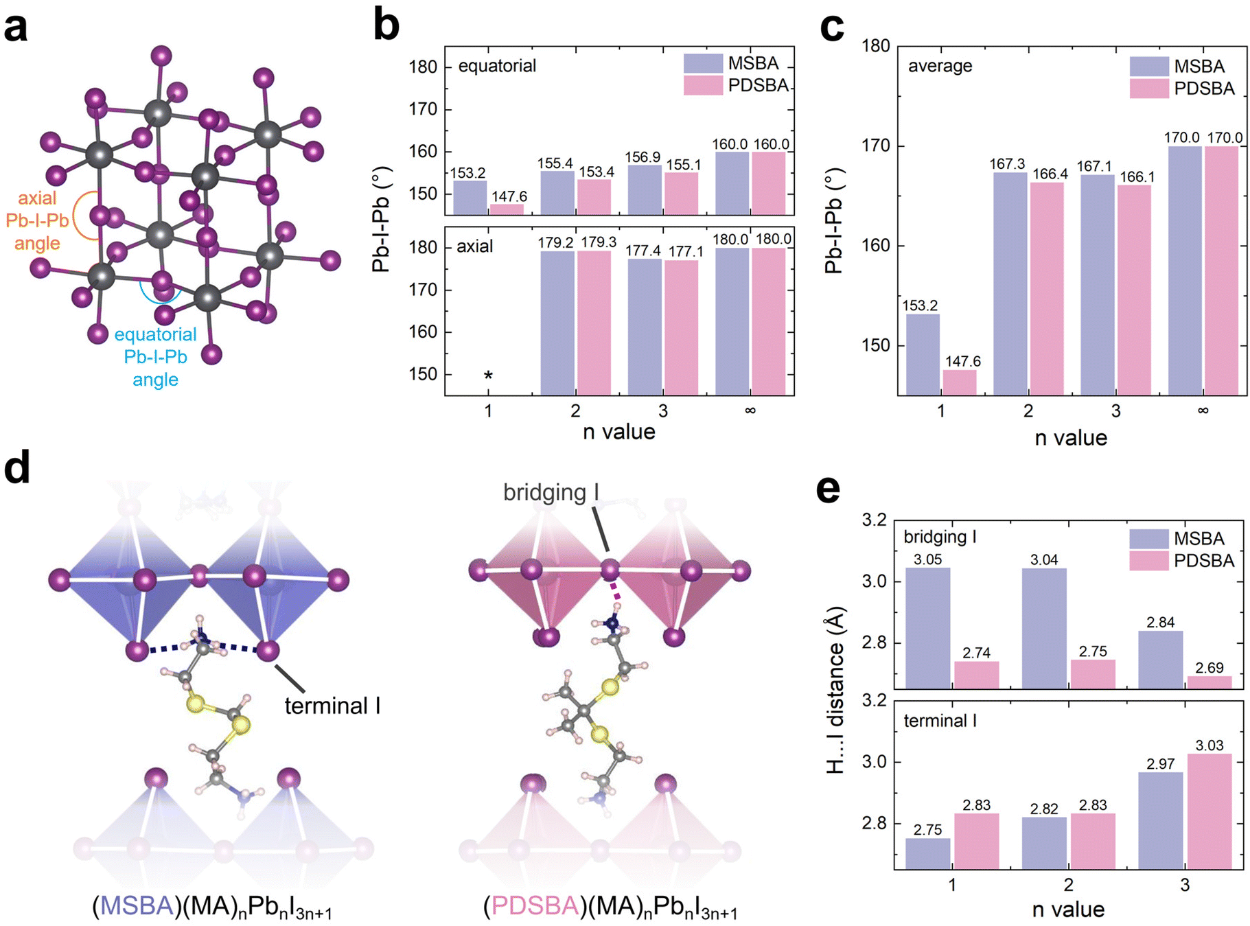 | ||
| Fig. 2 Structural analysis of (MSBA)(MA)n−1PbnI3n+1 and (PDSBA)(MA)n−1PbnI3n+1 (n = 1–3). (a) Definition of the axial Pb–I–Pb angles (marked in orange) and the equatorial Pb–I–Pb angles (marked in blue). (b) Equatorial, axial and (c) average Pb–I–Pb angles in (MSBA)(MA)n−1PbnI3n+1 and (PDSBA)(MA)n−1PbnI3n+1 (n = 1–3). There is no axial Pb–I–Pb angle in n = 1 structures, which is denoted using an asterisk (*). (d) Schematics of two types of H⋯I hydrogen bonds within DJ MHPs. The interactions between the NH3+ end groups and the terminal I and bridging I atoms are highlighted with blue and purple dashed lines, respectively. (e) The changes of the H⋯I distance defined in (d) with respect to the increase of the n value within the two series of RD MHPs. | ||
We next investigated the interaction between the diammonium cations and the inorganic layers, which is primarily due to the strong electrostatic interaction between the ammonium end groups and two types of I atoms on the boundary of the inorganic layer, i.e., the terminal I and the bridging I atoms (Fig. 2d). The distances between the H atom on the NH3+ groups and the adjacent I atoms are shown in Fig. 2e (ranging from 2.69 Å to 3.05 Å), which are shorter than the summation of the van der Waals radii of H and I atoms (ca. 3.1 Å) and thus can be attributed to the formation of hydrogen bonds. Following the increase in the n value, the distance between the H atom and the terminal I atom increases (from 2.75 Å to 2.97 Å for the MSBA series and from 2.83 Å to 3.03 Å for the PDSBA series). We ascribe this to the gradual reduction of in-plane distortion of the inorganic layer, which is in good agreement with the equatorial Pb–I–Pb angles mentioned above. The distortion allows more flexibility in the interface configuration and hence allows stronger hydrogen bonds between the surface I and the ammonium end groups.
The optical band gaps of the single crystals are shown in Fig. 3c. Similar to other reported RD structures,12,22,26 the increase in the n value results in the reduced bandgap of both types of DJ structures (MSBA: n = 1, 2.20 eV; n = 2, 2.02 eV; n = 3, 1.81 eV and PDSBA: n = 1, 2.29 eV; n = 2, 2.04 eV; n = 3: 1.83 eV). The bandgaps of (PDSBA)PbI4 are slightly larger than those of (MSBA)PbI4. This is expected because the distances between the inorganic layers of the MSBA series (from 5.93 to 5.64 Å) are significantly larger than those of the PDSBA series (from 7.36 to 7.04 Å), see Fig. 3d. Larger distances reduce the interlayer interaction, which is mediated by the organic cations, and hence reduce the widths of the valence band and the conduction band. Consequently, the band gap is enhanced.
 | ||
| Fig. 3 Optical properties of the MSBA-based and PDSBA-based MHPs. (a and b) Absorption spectra of the DJ MHP crystals (n = 1, 2, and 3) and (c) summary of the corresponding optical bandgaps. (d) Interlayer distances of the DJ MHPs as functions of n values; the interlayer distance refers to the distance between two adjacent inorganic layers (marked with a purple arrow). | ||
To gain insight into the electronic structures of RD MHPs, we turned to density functional theory (DFT) calculations. The calculated density of states (DOS) and atomic projected density of states (pDOS) are shown in Fig. 4. The calculated band gaps (MSBA: n = 1, 2.10 eV; n = 2, 1.88 eV; n = 3, 1.88 eV and PDSBA: n = 1, 2.20 eV; n = 2, 2.07 eV; n = 3, 1.90 eV) are in good agreement with the aforementioned optical bandgaps and the literature, where the band gaps of the MSBA series are systematically smaller than those of the PDSBA series. The bandgap of ∼1.88 eV for n = 2, 3 of the MSBA series shall not bother us. Despite the identical gaps, the DOS at the conduction band minimum is undoubtedly more pronounced for the n = 3 structure, indicating the trend of band gap reduction. It is important to note that both the CBM and valence band maximum (VBM) are dominated by lead and iodide atoms in the inorganic layer of both types of MHPs regardless of the n value, suggesting that the I and Pb atoms are primarily responsible for conducting holes and electrons in both series of DJ structures. Similar to the RD MHPs,26 the VB and CB DOS are increasingly dominated by the pDOS of I and Pb atoms following the increase in the n value in both series of MHPs, suggesting that the inorganic components (i.e., the PbnI3n+1 layers) serve as the main charge transport media.
 | ||
| Fig. 4 Electronic properties of PDSBA-based and MSBA-based MHPs. DOS and pDOS plots of (a) (MSBA)(MA)n−1PbnI3n+1 and (b) (PDSBA)(MA)n−1PbnI3n+1, where n = 1–3. | ||
To further understand the distribution of organic and inorganic components in the layered structures, we prepared a series of MHP polycrystalline films via a spin-cast process (see the Experimental section for more details). The powder X-ray diffraction (PXRD) results show distinct patterns of (h00), (0k0), and (00l) orientations for MSBA-based and PDSBA-based films with 〈n〉 values below 3, respectively (Fig. 5a and d), indicating that the inorganic components are oriented parallel to the substrate.10,27,28 Overall, the growth orientation of the layered structures with low 〈n〉 values is similar to the commonly reported RD MHPs,26 suggesting that these MHPs undergo a similar kinetic process during the polycrystalline film formation. As for the polycrystalline films with 〈n〉 values above 3, the PXRD results show the emergence of multiple signals that cannot be assigned to any specific RD phase, indicating the coexistence of layered inorganic components with different thicknesses and random growth orientations. Two intense signals at 14.2° and 28.5° can be found from the MHP films with 〈n〉 = 2, 3, and 5, which can be assigned to the (110) and (220) lattice planes of the bulk-like inorganic layers.29 These features indicate the presence of perpendicular-standing inorganic components, which are believed to benefit the charge transport of the MHP thin films for photovoltaic and light-emitting applications.30
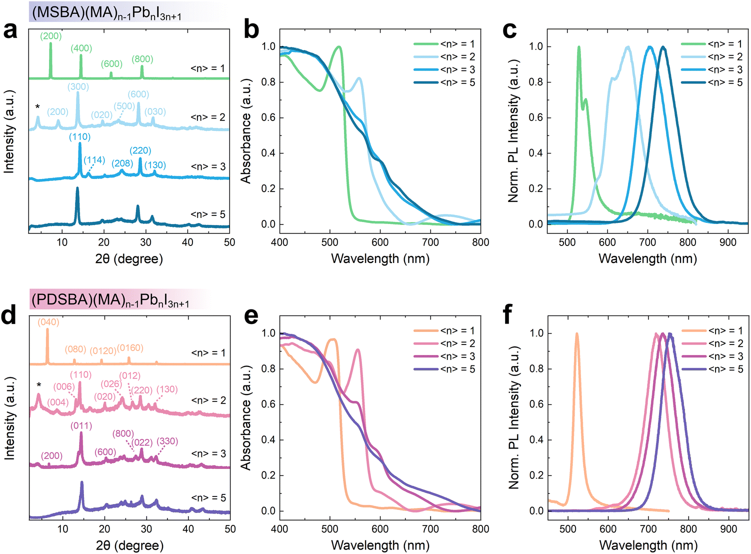 | ||
| Fig. 5 Structure and optical characterization of PDSBA-based and MSBA-based MHP thin films. (a) XRD patterns, (b) absorbance spectra, and (c) PL spectra of the (MSBA)(MA)n−1PbnI3n+1 thin films with 〈n〉 = 1–3. (d) XRD patterns, (e) absorbance spectra, and (f) PL spectra of the (PDSBA)(MA)n−1PbnI3n+1 thin films with 〈n〉 = 1–3. For the clarity of description, the value n represents the number of [PbI6]4−octahedra layers in a single MHP crystal. In contrast, symbol 〈n〉 is used to identify the average number of the layer of [PbI6]4− octahedra in an MHP polycrystal assembly such as the spin-coated thin films in this study. | ||
To experimentally confirm the photophysical properties of the DJ type polycrystalline film, we measured the absorption and photoluminescence (PL) spectra of the MHP thin films. A red-shift of the absorption edge is observed for both MSBA-based and PDSBA-based MHPs following the increase in the 〈n〉 value (MSBA: from 539 nm (〈n〉 = 1) to 721 nm (〈n〉 = 5) and PDSBA: from 531 nm (〈n〉 = 1) to 739 nm (〈n〉 = 5), Fig. 5b and e). These results are expected due to the increase in the thickness of the inorganic layers and are consistent with the trend of the calculated electronic band gaps. Small absorption features at 565 nm and 555 nm, found from the spectra of the samples with 〈n〉 = 3 and 5, can be assigned to the distinctive (MSBA)(MA)Pb2I7 and (PDSBA)(MA)Pb2I7, respectively. These absorption features confirm the coexistence of layered structures with different thicknesses. The absorption edges are shifted to 721 nm and 739 nm for (MSBA)(MA)4Pb5I16 and (PDSBA)(MA)4Pb5I16, respectively, which are dominated by the bulk-like absorption feature at 760–780 nm,26 consistent with RD MHPs with other large organic cations.22
Comparison of the absorption and PL spectra clearly shows a regular Stokes shift in the emission of (MSBA)PbI4 and (PDSBA)PbI4 thin films, consistent with other reported DJ type MHP structures.22 As for (MSBA)PbI4, two emission maxima are present in the PL results. The dual emission maxima may result from self-trapped excitons (STEs) which are dependent on lattice deformation, involving interactions between inorganic skeletons and organic cations to consequently affect electron–phonon coupling.31,32 Due to the decrease in the bandgap, an evident red-shift of the PL maxima can be clearly seen from those thin films following the increase in the 〈n〉 value (MSBA: from 529 nm to 737 nm and PDSBA: from 522 nm to 755 nm, Fig. 5c and f). The corresponding PL spectra also show the compositional evolution of the assembly of the inorganic components with various thicknesses of the inorganic layer. Specifically, a more rapid red-shift of the PL signals was observed from the thin film samples of the PDSBA series following the increase in the 〈n〉 value compared to their MSBA-based counterparts (Fig. 5c and f). This may be because of the difference in the population distribution of quantum well thicknesses within those thin films.11,12 It is therefore reasonable to speculate that the PDSBA cations assist in the formation of multicrystalline thin films containing RD MHP domains with a narrower distribution of n values.28
The evolution of the emission patterns of the DJ type MHPs with relatively large 〈n〉 values (e.g., 〈n〉 = 3 and 5) drove us to further investigate the corresponding electroluminescence (EL) of those MHPs in the near-infrared region. We constructed LEDs with the architecture shown in Fig. 6a.33 ZnO nanoparticles (NPs) and poly-(9,9-dioctylfluorenyl-2,7-diyl)-alt-(4,4′-(N-(4-butylphenyl))) (TFB) were used as the electron transport layer (ETL) and hole transport layer (HTL), respectively. Cross-sectional scanning electron microscopy (SEM) imaging revealed that the thicknesses of the layers of ZnO NPs, MHP films, and TFB are around 30 nm, 175 nm, and 35 nm, respectively (Fig. S6†).
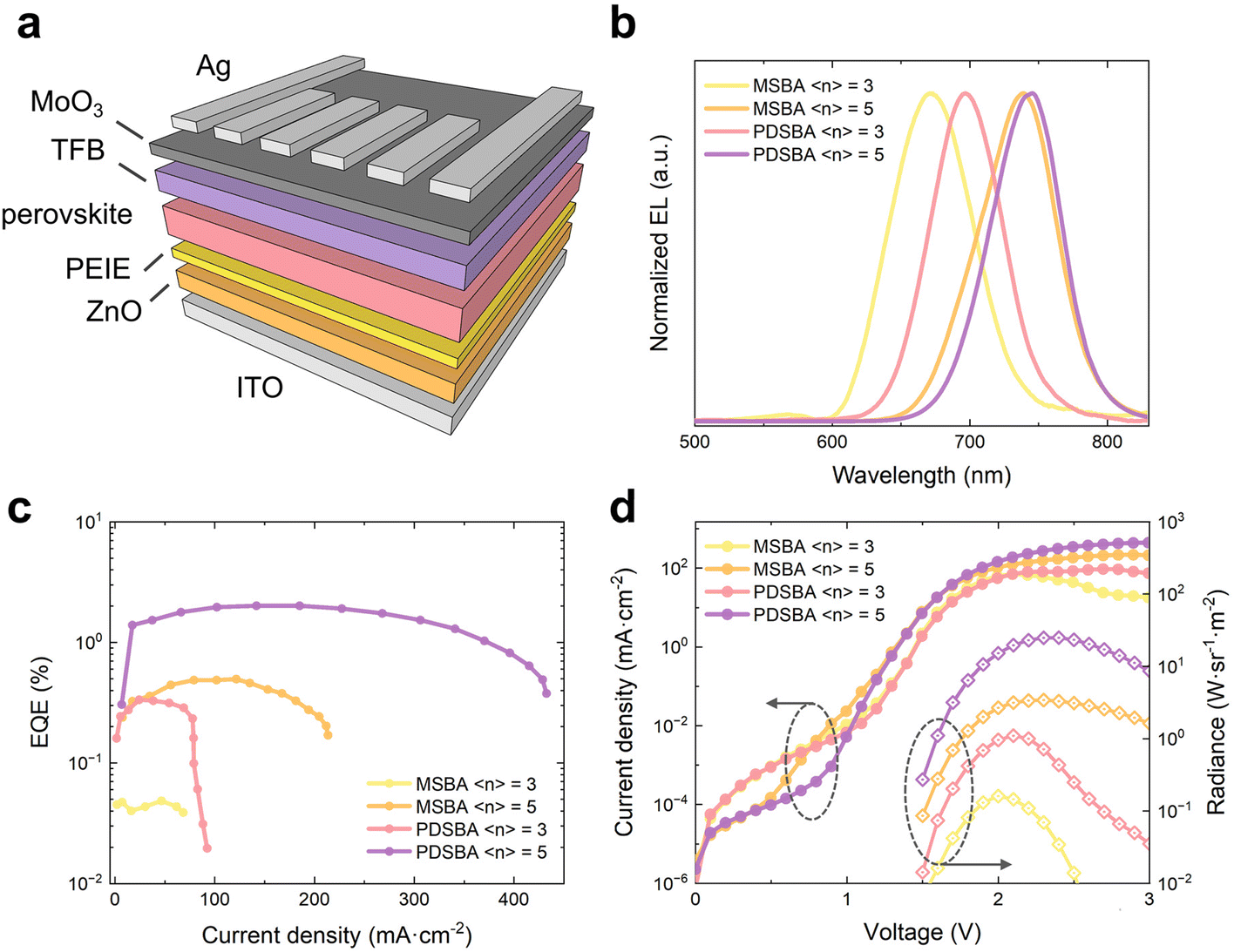 | ||
| Fig. 6 Device structure and the performance of the MHP LEDs. (a) General device architecture used in this study. (b) EL spectra from DJ type MHP devices with various 〈n〉 values and cation types. (c) The corresponding EQE results and (d) current density versus voltage and radiance plots of the DJ MHP devices with various cations and 〈n〉 values. | ||
We next investigated the performance of the corresponding devices. The EL maxima of all devices were around 671 nm and 746 nm (Fig. 6b), an approximately 0–38 nm blue-shift with respect to the corresponding PL spectra.34 We obtained the champion device based on 〈n〉 = 5 PDSBA-based MHP devices with a relatively low turn-on voltage of 1.5 V (Fig. 6d). The EQE maximum of the corresponding device was 2.0% at 2.0 V with a current density of ∼140 mA cm−2 (Fig. 6c), and a radiance value of 25 W sr−1 cm−2 (corresponding radiant flux: 6.3 × 10⁻⁴ W) was achieved at 2.4 V.
Conclusion
We herein investigated two series of new Dion–Jacobson type metal halide perovskites (MHPs) with dithioketal-containing organic cations. The reduced-dimensional (RD) MHP single crystals were prepared using a single-step temperature-lowering nucleation process, in which the organothiol-containing cations convert to dithioketal diammonium intercalating cations simultaneously. The thickness and the stacking mode of the inorganic components can be effectively tailored in the RD structures in both single-crystal and thin film forms by changing the precursor ratios, yielding materials with bright PLs across a broad spectral range. The device performance strongly depends on the type of cation and the number of layers of the inorganic frameworks in the RD MHPs. The optimized NIR-emitting devices show improved external quantum efficiency of up to 2.0% and a radiance value of 25 W sr−1 cm−2. Further efforts will be warranted in optimizing intercalating cations and controlling the lattice orientation in RD MHP active layers.Author contributions
W. L. and Z. Y. designed this study and wrote the manuscript. W. L. conducted the synthesis and characterization of all compounds. G. Y., T. Z. and Y. Z. conducted the calculation. W. L., L. Z., S. H., C. L. and B. L. fabricated and characterized the devices. All authors have given approval to the final version of the manuscript.Conflicts of interest
There are no conflicts to declare.Acknowledgements
All calculations were carried out using the Tianhe-2 (TH-2) supercomputer clusters (Guangzhou, Guangdong, China) and resources provided by the Digital Research Alliance of Canada. Z. Y. would like to acknowledge financial support from the National Natural Science Foundation of China (no. 21905316, 22175201), the Department of Science and Technology of Guangdong Province (no. 2019QN01C108), and Sun Yat-sen University. T. Z. thanks York University for the start-up grant (no. 481333) and the Natural Sciences and Engineering Research Council (NSERC) of Canada (no. RGPIN-2016-06276) for financial support.References
- Z. Yuan, L. Zhao, E. Pradhan, M. Lai, T. Zeng and Z. Yang, Postsynthetic crystalline transformation in two-dimensional perovskites via organothiol-based chemistry, CCS Chem., 2022, 3, 1276–1284 Search PubMed.
- B. Saparov and D. B. Mitzi, Organic–inorganic perovskites: Structural versatility for functional materials design, Chem. Rev., 2016, 116, 4558–4596 CrossRef CAS PubMed.
- L. N. Quan, B. P. Rand, R. H. Friend, S. G. Mhaisalkar, T.-W. Lee and E. H. Sargent, Perovskites for next-generation optical sources, Chem. Rev., 2019, 119, 7444–7477 CrossRef CAS PubMed.
- X. Gao, X. Zhang, W. Yin, H. Wang, Y. Hu, Q. Zhang, Z. Shi, V. L. Colvin, W. W. Yu and Y. Zhang, Ruddlesden–Popper perovskites: Synthesis and optical properties for optoelectronic applications, Adv. Sci., 2019, 6, 1900941 CrossRef CAS PubMed.
- L. Zhang, C. Sun, T. He, Y. Jiang, J. Wei, Y. Huang and M. Yuan, High-performance quasi-2D perovskite light-emitting diodes: From materials to devices, Light: Sci. Appl., 2021, 10, 61 CrossRef CAS PubMed.
- D. Yang, B. Zhao, T. Yang, R. Lai, D. Lan, R. H. Friend and D. Di, Toward stable and efficient perovskite light-emitting diodes, Adv. Funct. Mater., 2022, 32, 2109495 CrossRef CAS.
- J. S. Kim, J.-M. Heo, G.-S. Park, S.-J. Woo, C. Cho, H. J. Yun, D.-H. Kim, J. Park, S.-C. Lee, S.-H. Park, E. Yoon, N. C. Greenham and T.-W. Lee, Ultra-bright, efficient and stable perovskite light-emitting diodes, Nature, 2022, 611, 688–694 CrossRef CAS PubMed.
- L. N. Quan, M. Yuan, R. Comin, O. Voznyy, E. M. Beauregard, S. Hoogland, A. Buin, A. R. Kirmani, K. Zhao, A. Amassian, D. H. Kim and E. H. Sargent, Ligand-stabilized reduced-dimensionality perovskites, J. Am. Chem. Soc., 2016, 138, 2649–2655 CrossRef CAS PubMed.
- L. Mao, C. C. Stoumpos and M. G. Kanatzidis, Two-dimensional hybrid halide perovskites: Principles and promises, J. Am. Chem. Soc., 2019, 141, 1171–1190 CrossRef CAS PubMed.
- X. Li, J. M. Hoffman and M. G. Kanatzidis, The 2D halide perovskite rulebook: how the spacer influences everything from the structure to optoelectronic device efficiency, Chem. Rev., 2021, 121, 2230–2291 CrossRef CAS PubMed.
- N. Wang, C. Lu, G. Rui, S. Zhang and H. Wei, Perovskite light-emitting diodes based on solution-processed self-organized multiple quantum wells, Nat. Photonics, 2016, 10, 699–704 CrossRef CAS.
- M. Yuan, L. N. Quan, R. Comin, G. Walters, R. Sabatini, O. Voznyy, S. Hoogland, Y. Zhao, E. M. Beauregard, P. Kanjanaboos, Z. Lu, D. H. Kim and E. H. Sargent, Perovskite energy funnels for efficient light-emitting diodes, Nat. Nanotechnol., 2016, 11, 872–877 CrossRef CAS PubMed.
- T. Niu, Q. Xue and H.-L. Yip, Advances in Dion–Jacobson phase two-dimensional metal halide perovskite solar cells, Nanophotonics, 2020, 10, 2069–2102 CrossRef.
- W. Guo, Z. Yang, J. Dang and M. Wang, Progress and perspective in Dion–Jacobson phase 2D layered perovskite optoelectronic applications, Nano Energy, 2021, 86, 106129 CrossRef CAS.
- H. Fu, Dion–Jacobson halide perovskites for photovoltaic and photodetection applications, J. Mater. Chem. C, 2021, 9, 6378–6394 RSC.
- D. B. Mitzi, Templating and structural engineering in organic–inorganic perovskites, J. Chem. Soc., 2001, 1–12 CAS.
- D. Pan, Y. Fu, N. Spitha, Y. Zhao, C. R. Roy, D. J. Morrow, D. D. Kohler, J. C. Wright and S. Jin, Deterministic fabrication of arbitrary vertical heterostructures of two-dimensional Ruddlesden–Popper halide perovskites, Nat. Nanotechnol., 2021, 16, 159–165 CrossRef CAS PubMed.
- D. Solis-Ibarra and H. I. Karunadasa, Reversible and irreversible chemisorption in nonporous–crystalline hybrids, Angew. Chem., 2014, 126, 1057–1060 CrossRef.
- C. Ortiz-Cervantes, P. I. Román-Román, J. Vazquez-Chavez, M. Hernández-Rodríguez and D. Solis-Ibarra, Thousand–fold conductivity increase in 2D perovskites by polydiacetylene incorporation and doping, Angew. Chem., 2018, 130, 14078–14082 CrossRef.
- I. Spanopoulos, I. Hadar, W. Ke, Q. Tu, M. Chen, H. Tsai, Y. He, G. Shekhawat, V. P. Dravid, M. R. Wasielewski, A. D. Mohite, C. C. Stoumpos and M. G. Kanatzidis, Uniaxial expansion of the 2D Ruddlesden–Popper perovskite family for improved environmental stability, J. Am. Chem. Soc., 2019, 141, 5518–5534 CrossRef CAS PubMed.
- D. B. Mitzi, K. Chondroudis and C. R. Kagan, Design, structure, and optical properties of organic−inorganic perovskites containing an oligothiophene chromophore, Inorg. Chem., 1999, 38, 6246–6256 CrossRef CAS PubMed.
- L. Mao, W. Ke, L. Pedesseau, Y. Wu, C. Katan, J. Even, M. R. Wasielewski, C. C. Stoumpos and M. G. Kanatzidis, Hybrid Dion–Jacobson 2D lead iodide perovskites, J. Am. Chem. Soc., 2018, 140, 3775–3783 CrossRef CAS PubMed.
- X. Li, W. Ke, B. Traoré, P. Guo, I. Hadar, M. Kepenekian, J. Even, C. Katan, C. C. Stoumpos, R. D. Schaller and M. G. Kanatzidis, Two-dimensional Dion–Jacobson hybrid lead iodide perovskites with aromatic diammonium cations, J. Am. Chem. Soc., 2019, 141, 12880–12890 CrossRef CAS PubMed.
- Y. Shang, Y. Liao, Q. Wei, Z. Wang, B. Xiang, Y. Ke, W. Liu and Z. Ning, Highly stable hybrid perovskite light-emitting diodes based on Dion–Jacobson structure, Sci. Adv., 2019, 5, eaaw8072 CrossRef CAS PubMed.
- L. Gao, X. Li, B. Traoré, Y. Zhang, J. Fang, Y. Han, J. Even, C. Katan, K. Zhao, S. Liu and M. G. Kanatzidis, m-Phenylenediammonium as a new spacer for Dion–Jacobson two-dimensional perovskites, J. Am. Chem. Soc., 2021, 143, 12063–12073 CrossRef CAS PubMed.
- C. Ni, Y. Huang, T. Zeng, D. Chen, H. Chen, M. Wei, A. Johnston, A. H. Proppe, Z. Ning and E. H. Sargent, Thiophene cation intercalation to improve band–edge integrity in reduced-dimensional perovskites, Angew. Chem., 2020, 132, 14081–14087 CrossRef.
- H. Tsai, W. Nie, J.-C. Blancon, C. C. Stoumpos, R. Asadpour, B. Harutyunyan, A. J. Neukirch, R. Verduzco, J. J. Crochet, S. Tretiak, L. Pedesseau, J. Even, M. A. Alam, G. Gupta, J. Lou, P. M. Ajayan, M. J. Bedzyk, M. G. Kanatzidis and A. D. Mohite, High-efficiency two-dimensional Ruddlesden–Popper perovskite solar cells, Nature, 2016, 536, 312–316 CrossRef CAS PubMed.
- R. Quintero-Bermudez, A. Gold-Parker, A. H. Proppe, R. Munir, Z. Yang, S. O. Kelley, A. Amassian, M. F. Toney and E. H. Sargent, Compositional and orientational control in metal halide perovskites of reduced dimensionality, Nat. Mater., 2018, 17, 900–907 CrossRef CAS PubMed.
- A. Z. Chen, B. J. Foley, J. H. Ma, M. R. Alpert, J. S. Niezgoda and J. J. Choi, Crystallographic orientation propagation in metal halide perovskite thin films, J. Mater. Chem. A, 2017, 5, 7796–7800 RSC.
- T. Zhou, H. Lai, T. Liu, D. Lu, X. Wan, X. Zhang, Y. Liu and Y. Chen, Highly efficient and stable solar cells based on crystalline oriented 2D/3D hybrid perovskite, Adv. Mater., 2019, 31, 1901242 CrossRef PubMed.
- Y. Han, J. Yin, G. Cao, Z. Yin, Y. Dong, R. Chen, Y. Zhang, N. Li, S. Jin, O. F. Mohammed, B.-B. Cui and Q. Chen, Exciton self-trapping for white emission in 100-oriented two-dimensional perovskites via halogen substitution, ACS Energy Lett., 2022, 7, 453–460 CrossRef CAS.
- S. Kahmann, D. Meggiolaro, L. Gregori, E. K. Tekelenburg, M. Pitaro, S. D. Stranks, F. De Angelis and M. A. Loi, The origin of broad emission in 〈100〉 two-dimensional perovskites: Extrinsic vs intrinsic processes, ACS Energy Lett., 2022, 7, 4232–4241 CrossRef CAS PubMed.
- J. Wang, N. Wang, Y. Jin, J. Si, Z. K. Tan, H. Du, L. Cheng, X. Dai, S. Bai and H. He, Interfacial control toward efficient and low-voltage perovskite light-emitting diodes, Adv. Mater., 2015, 27, 2311–2316 CrossRef CAS PubMed.
- Z. Xiao, R. A. Kerner, L. Zhao, N. L. Tran, K. M. Lee, T.-W. Koh, G. D. Scholes and B. P. Rand, Efficient perovskite light-emitting diodes featuring nanometre-sized crystallites, Nat. Photonics, 2017, 11, 108–115 CrossRef CAS.
Footnote |
| † Electronic supplementary information (ESI) available. CCDC 2249121, 2249140–2249143. For ESI and crystallographic data in CIF or other electronic format see DOI: https://doi.org/10.1039/d3qi01512b |
| This journal is © the Partner Organisations 2023 |