 Open Access Article
Study of Se/Te-doped Cu2O as a hole transport material in perovskite solar cells
Liang Luo a,
Bao Zhou*a,
Zhenzhen Liua,
Qirong Zhaoa,
Chao Wanga,
Zhuoqi Duana,
Zaixin Xiea,
Xiaobo Yangb and
Yongmao Hu
 ab
ab
aCollege of Engineering, Dali University, Dali, Yunnan 671003, China. E-mail: zhoubao@dali.edu.cn
bFaculty of Materials Science and Engineering, Kunming University of Science and Technology, Kunming 650093, China
First published on 14th March 2023
Abstract
Theoretically, cuprous oxide (Cu2O) is a particularly excellent potential material, for the hole transport layer (HTL) of perovskite solar cells (PSCs). However, the photoelectric conversion efficiency (PCE) of its experimental samples is still not ideal. The main reasons for this include the material, and inherent and interface defects of Cu2O, but this can be improved by doping. In this research, Te- and Se/Te-doped Cu2O were experimentally and numerically studied to check the improvement of the material and interface properties. It was found that, for both the electrical and optical properties, the Se/Te-doped Cu2O performed considerably better than that which had been Te-doped and the pure Cu2O. Compared with the pure Cu2O thin film, the carrier mobility of the Se/Te-doped Cu2O thin film is improved from 60 cm2 V−1 s−1 to 1297 cm2 V−1 s−1, and the bandgap changed from 2.05 eV to 1.88 eV. According to the results calculated using solar cell simulation software SCAPS, the cell efficiency of the Se/Te-doped Cu2O is improved by 22% when compared to that of pure Cu2O. This efficiency can be further improved to 34% by optimizing the thickness of the Se/Te-doped Cu2O thin film and the defect density of states between the material interfaces.
1 Introduction
Cuprous oxide (Cu2O) has good practical applications in fungicides, photocatalysis and solar cells because of its bandgap (2.0–2.2 eV), high light absorption coefficient, stable chemical properties, and so on.1–3 For perovskite solar cells (PSCs), Cu2O is an excellent inorganic material as the hole transport layer (HTL) because of its stability, inexpensiveness and ease of preparation when compared with organic materials, such as spiro-OMeTAD. Theoretically the photoelectric conversion efficiency (PCE) of Cu2O-based PSCs can be as high as 28%,4 but is found to be only about 18%,5–7 experimentally, because of the material and interface defects, and difficulties with the preparation process. Tseng et al.8 prepared Ag/GZO/SiO2/MAPbI3/Cu2O/FTO reverse-structured PSCs by controlling the annealing temperature and deposition thickness of hole transport layer (HTL) and electron transport level (ETL), and the highest PCE found reached 18.4%. Liu et al.9 prepared FTO/TiO2/Cs0.05FA0.81MA0.14PbI2.55Br0.45/Cu2O/Au forward-structured PSCs with a surface modification of Cu2O quantum dot films, and the PCE was improved to 18.9%, and the efficiency was still more than 90% of the initial one after 30 d of preservation. The interface performance between the perovskite active layer (PAL, mainly MAPbI3, FAPbI3 and their derivatives) and HTL is very important. In addition to changing the preparation method and adding interface modification materials, it is also possible to improve the PCE of the solar cell by doping.Some studies have shown that Se and Te doping can effectively reduce the crystal bandgap of the metal oxide materials, increase their light absorption range, improve their light absorption coefficient, and improve their carrier mobility and other properties. For example, Lin et al.10 prepared nanotubes with different ratios of Te and Se/Te doped TiO2, and found that the absorption coefficient was considerably enhanced in the visible spectrum, and the absorption edge had a strong red shift. Güney and Duman11 prepared ZnSeO and ZnTeO thin films by changing the doping ratios of Se and Te, and obtained a significant decrease from 3.37 eV (pure ZnO) to 2.26–2.60 eV. Liu et al.12 studied S-, Se- and Te-doped NaTaO3 using the first-principles calculations, and obtained similar results for bandgap, in addition, the carrier mobility, and its difference between electrons and holes, was all significantly larger than that of pure NaTaO3, which could effectively reduce the recombination of electrons and holes. Based on the previous work, it is also known that Te-doped Cu2O can effectively reduce its bandgap and improve its conductivity.13 However, the disadvantage of using Te is its biological toxicity. He and Su14 found that alloying Te with Se (Te![[thin space (1/6-em)]](https://www.rsc.org/images/entities/char_2009.gif) :
:![[thin space (1/6-em)]](https://www.rsc.org/images/entities/char_2009.gif) Se = 1
Se = 1![[thin space (1/6-em)]](https://www.rsc.org/images/entities/char_2009.gif) :
:![[thin space (1/6-em)]](https://www.rsc.org/images/entities/char_2009.gif) 0.43) could entirely eliminate the Te biological toxicity. This research focused on the photovoltaic properties of Se/Te-doped Cu2O and complete simulations of its use as PSCs. Firstly, the electrical and optical properties of Te- and Se/Te-doped Cu2O were calculated theoretically. Then, the corresponding films were prepared experimentally to validate the theoretical results. Finally, the PSCs based on different HTLs (made of Te- and Se/Te-doped Cu2O thin films) were modelled and simulated using SCAPS software to check their performances.
0.43) could entirely eliminate the Te biological toxicity. This research focused on the photovoltaic properties of Se/Te-doped Cu2O and complete simulations of its use as PSCs. Firstly, the electrical and optical properties of Te- and Se/Te-doped Cu2O were calculated theoretically. Then, the corresponding films were prepared experimentally to validate the theoretical results. Finally, the PSCs based on different HTLs (made of Te- and Se/Te-doped Cu2O thin films) were modelled and simulated using SCAPS software to check their performances.
2 Theoretical research
2.1 Models and calculation
The structural models can be seen in Fig. 1(a). Firstly, a 2 × 2 × 1 Cu2O supercell, consisting of a total of 16 Cu atoms and 8 O atoms was constructed. Secondly, the positions of the three O atoms in the supercell were replaced with Te atoms to give Te![[thin space (1/6-em)]](https://www.rsc.org/images/entities/char_2009.gif) :
:![[thin space (1/6-em)]](https://www.rsc.org/images/entities/char_2009.gif) Cu2O, with a Te content of 12.5%, as shown in Fig. 1(b). Lastly, by replacing one of the Te atoms in the center of supercell, with a Se atom to give Se/Te
Cu2O, with a Te content of 12.5%, as shown in Fig. 1(b). Lastly, by replacing one of the Te atoms in the center of supercell, with a Se atom to give Se/Te![[thin space (1/6-em)]](https://www.rsc.org/images/entities/char_2009.gif) :
:![[thin space (1/6-em)]](https://www.rsc.org/images/entities/char_2009.gif) Cu2O, the proportion of the Se atoms was 4.17%, and the proportion of the rest of the Te atoms was 8.33%, as shown in Fig. 1(c). The electrical and optical properties of Cu2O before and after doping were obtained using first-principles calculations, and the changes in the material properties were compared.
Cu2O, the proportion of the Se atoms was 4.17%, and the proportion of the rest of the Te atoms was 8.33%, as shown in Fig. 1(c). The electrical and optical properties of Cu2O before and after doping were obtained using first-principles calculations, and the changes in the material properties were compared.
2.2 Calculation results and discussion
| α (°) | β (°) | γ (°) | a (Å) | b (Å) | c (Å) | Volume (Å3) | Total energy (eV) | |
|---|---|---|---|---|---|---|---|---|
| Cu2O | 90 | 90 | 90 | 4.22 | 8.46 | 8.46 | 301.39 | −27036.35 |
Te![[thin space (1/6-em)]](https://www.rsc.org/images/entities/char_2009.gif) : :![[thin space (1/6-em)]](https://www.rsc.org/images/entities/char_2009.gif) Cu2O Cu2O |
78.27 | 89.97 | 89.94 | 5.41 | 8.54 | 8.53 | 385.82 | −26396.01 |
Se/Te![[thin space (1/6-em)]](https://www.rsc.org/images/entities/char_2009.gif) : :![[thin space (1/6-em)]](https://www.rsc.org/images/entities/char_2009.gif) Cu2O Cu2O |
102.51 | 89.99 | 90.01 | 5.40 | 8.45 | 8.45 | 376.46 | −26433.76 |
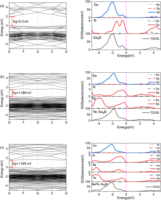
Fig. 2 shows the band structures and DOS of the three systems. The calculated bandgap value of the pure Cu2O was 0.577 eV, the scissors operator was used and a correction value of 1.423 eV was given, and the experimental value of pure Cu2O was 2.0 eV,16,17 as shown in Fig. 2(a). The valence band maximum (VBM) and the conduction band minimum (CBM) were both located at the high symmetry point G, that is, the direct bandgap, and the DOS showed a similar distribution to the band structure. From Fig. 2(b), it can be seen that the bandgap of Te![[thin space (1/6-em)]](https://www.rsc.org/images/entities/char_2009.gif) :
:![[thin space (1/6-em)]](https://www.rsc.org/images/entities/char_2009.gif) Cu2O decreased to 1.489 eV from the 2.0 eV of pure Cu2O, which had reached the infrared region, and the Te 5p states were densely distributed at the Fermi level, which caused the O 2p states in the conduction band to move to the low energy end, and improve the localization of the electrons. From Fig. 2(c), it can be seen that the bandgap value of the Se/Te-doped Cu2O was increased to 1.545 eV when compared to that of the Te-doped Cu2O. It was also known from previous work that the Se-doped Cu2O can increase its bandgap.13
Cu2O decreased to 1.489 eV from the 2.0 eV of pure Cu2O, which had reached the infrared region, and the Te 5p states were densely distributed at the Fermi level, which caused the O 2p states in the conduction band to move to the low energy end, and improve the localization of the electrons. From Fig. 2(c), it can be seen that the bandgap value of the Se/Te-doped Cu2O was increased to 1.545 eV when compared to that of the Te-doped Cu2O. It was also known from previous work that the Se-doped Cu2O can increase its bandgap.13
The electron effective mass and hole effective mass for the three systems are shown in Table 2. As is known in μ = qτ/m*, a smaller effective mass (m*) implied a higher carrier mobility (μ). From the calculated values of the effective masses, the effective mass of pure Cu2O was basically consistent with that found in the literature.18,19 Compared with pure Cu2O, the electron effective mass and hole effective mass in the doped systems were significantly reduced, and the carrier mobility was higher. Among the three systems, the carrier mobility of Se/Te![[thin space (1/6-em)]](https://www.rsc.org/images/entities/char_2009.gif) :
:![[thin space (1/6-em)]](https://www.rsc.org/images/entities/char_2009.gif) Cu2O increased more significantly.
Cu2O increased more significantly.
| Cu2O | Te![[thin space (1/6-em)]](https://www.rsc.org/images/entities/char_2009.gif) : :![[thin space (1/6-em)]](https://www.rsc.org/images/entities/char_2009.gif) Cu2O Cu2O |
Se/Te![[thin space (1/6-em)]](https://www.rsc.org/images/entities/char_2009.gif) : :![[thin space (1/6-em)]](https://www.rsc.org/images/entities/char_2009.gif) Cu2O Cu2O |
Cu2O [18] | Cu2O [19] | |
|---|---|---|---|---|---|
| CBM | 0.7358l | 0.4174 | 0.3754 | 0.6535 | 0.676 |
| VBM | 2.7762 | 0.651 | 0.5643 | 2.4015 | 3.80 |
The Mulliken populations of the central atoms and their adjacent atoms for the three systems are shown in Table 3. From the charge population in pure Cu2O, it was seen that each Cu loses 0.32e, and O gains 0.63e. For the Te-doped Cu2O, the Te loses 1.36e, the adjacent Cu gains 0.14e, and the next-adjacent O gains 0.66e. This shows that after Te doping, there was at least one free electron that caused the doped system to be metallized. For the Se/Te-doped Cu2O, the Te shows a stronger ability to lose electrons, losing 1.57e, the central Se loses 0.81e, the adjacent Cu gains 0.1e, and the next adjacent O gains 0.64e. The Te has the most pronounced ability to lose electrons and becomes the center of the accumulation of the positive charges, which improved electron transport capacity and enhanced the electrical conductivity better than pure Cu2O did. According to the bond population, the Cu–O population of pure Cu2O was 0.38, which indicated a strong interaction between the Cu and O atoms, and the presence of covalent bonds. With the doping of Te and Se/Te, the Cu–O bond population decreased, the covalence became weaker, and the bond length increased from 1.83 Å to 1.87 Å. The bond lengths of Cu–Te and Cu–Se were about 2.44 Å and 2.24 Å, respectively, which were much larger than the Cu–O bond length, which was the main reason for the lattice distortion of the doped systems.
![[thin space (1/6-em)]](https://www.rsc.org/images/entities/char_2009.gif) :
:![[thin space (1/6-em)]](https://www.rsc.org/images/entities/char_2009.gif) Cu2O, and Se/Te
Cu2O, and Se/Te![[thin space (1/6-em)]](https://www.rsc.org/images/entities/char_2009.gif) :
:![[thin space (1/6-em)]](https://www.rsc.org/images/entities/char_2009.gif) Cu2O
Cu2O
| Charge population (e) | Bond population/bond length (Å) | |||||||
|---|---|---|---|---|---|---|---|---|
| Cu | O | Se | Te | Cu–O | Cu–Se | Cu–Te | ||
| Cu2O | 0.32 | −0.63 | — | — | 0.38/1.83 | — | — | |
Te![[thin space (1/6-em)]](https://www.rsc.org/images/entities/char_2009.gif) : :![[thin space (1/6-em)]](https://www.rsc.org/images/entities/char_2009.gif) Cu2O Cu2O |
−0.14 | −0.66 | — | 1.36 | 0.37/1.87 | — | −0.19/2.43 | |
Se/Te![[thin space (1/6-em)]](https://www.rsc.org/images/entities/char_2009.gif) : :![[thin space (1/6-em)]](https://www.rsc.org/images/entities/char_2009.gif) Cu2O Cu2O |
−0.10 | −0.64 | 0.81 | 1.57 | 0.32/1.87 | 0.06/2.24 | −0.43/2.44 | |
3 Experimental research
3.1 Experiment methods
The theoretical results showed that when the ratios of Te- and Se/Te-doped Cu2O was 12.5%, the bandgap can reach the infrared region. However, the bandgap of HTL was smaller than that of the PAL (MAPbI3 band gap value of 1.55 eV), which could not take the role of the conduction band to block electrons. Therefore, when preparing samples, the doping ratio was reduced to make the bandgap slightly larger than that of the PAL, and the doping ratio is shown in Table 4. In this experiment, the powders were prepared by solid-phase sintering synthesis,20,21 and the thin films were prepared by a spin-coating method. The naming of the experimental samples is consistent with that in the theoretical research.| Cu2O | Te | Se | Doping ratio | |
|---|---|---|---|---|
Te![[thin space (1/6-em)]](https://www.rsc.org/images/entities/char_2009.gif) : :![[thin space (1/6-em)]](https://www.rsc.org/images/entities/char_2009.gif) Cu2O Cu2O |
2.5 mmol | 0.2 mmol | — | 7.4% |
Se/Te![[thin space (1/6-em)]](https://www.rsc.org/images/entities/char_2009.gif) : :![[thin space (1/6-em)]](https://www.rsc.org/images/entities/char_2009.gif) Cu2O Cu2O |
2.5 mmol | 0.2 mmol | 0.1 mmol | 10.71% |
3.2 Experimental results and discussion
 | ||
Fig. 4 The XRD of (a) pure Cu2O, Te![[thin space (1/6-em)]](https://www.rsc.org/images/entities/char_2009.gif) : :![[thin space (1/6-em)]](https://www.rsc.org/images/entities/char_2009.gif) Cu2O, and Se/Te Cu2O, and Se/Te![[thin space (1/6-em)]](https://www.rsc.org/images/entities/char_2009.gif) : :![[thin space (1/6-em)]](https://www.rsc.org/images/entities/char_2009.gif) Cu2O powders, and (b) Te Cu2O powders, and (b) Te![[thin space (1/6-em)]](https://www.rsc.org/images/entities/char_2009.gif) : :![[thin space (1/6-em)]](https://www.rsc.org/images/entities/char_2009.gif) Cu2O and Se/Te Cu2O and Se/Te![[thin space (1/6-em)]](https://www.rsc.org/images/entities/char_2009.gif) : :![[thin space (1/6-em)]](https://www.rsc.org/images/entities/char_2009.gif) Cu2O thin films. Cu2O thin films. | ||
For the XPS, the corrected standard C 1s peak position (284.8 eV) is shown in Fig. 5. The peaks of four elements Cu, O, Se, and Te were found, and are identified on the full spectrum shown in Fig. 5(a). Compared with the Te![[thin space (1/6-em)]](https://www.rsc.org/images/entities/char_2009.gif) :
:![[thin space (1/6-em)]](https://www.rsc.org/images/entities/char_2009.gif) Cu2O powder, the peak intensities of Cu 2p and Te 3d of the Se/Te
Cu2O powder, the peak intensities of Cu 2p and Te 3d of the Se/Te![[thin space (1/6-em)]](https://www.rsc.org/images/entities/char_2009.gif) :
:![[thin space (1/6-em)]](https://www.rsc.org/images/entities/char_2009.gif) Cu2O powder were significantly weakened. Semi-quantitative composition analysis proved that the proportion of Cu and Te was indeed reduced, which was also confirmed by the subsequent EDS analysis. The two splitting peaks of Cu 2p are Cu 2p1/2 and Cu 2p3/2, and their binding energy positions were about 952.52 eV and 932.76 eV, respectively, which were Cu1+. There was only one obvious peak for O 1s, and its binding energy position was about 532.18 eV, which was O2−. The two splitting peaks of Te 3d were Te 3d3/2 and Te 3d5/2, and their binding energy positions were about 583.15 eV and 572.78 eV, respectively, which were Te+4. The two peaks near 586.54 eV and 576.04 eV were peaks formed by Te–O bonds, which proved that part of Te occupied the Cu vacancies. There was only one obvious peak for Se 3d, and its binding energy position was about 54.56 eV, which was Se4+. The peak positions of the four elements, Cu, O, Se, and Te were basically consistent with those previously reported in the literature.10,22–24
Cu2O powder were significantly weakened. Semi-quantitative composition analysis proved that the proportion of Cu and Te was indeed reduced, which was also confirmed by the subsequent EDS analysis. The two splitting peaks of Cu 2p are Cu 2p1/2 and Cu 2p3/2, and their binding energy positions were about 952.52 eV and 932.76 eV, respectively, which were Cu1+. There was only one obvious peak for O 1s, and its binding energy position was about 532.18 eV, which was O2−. The two splitting peaks of Te 3d were Te 3d3/2 and Te 3d5/2, and their binding energy positions were about 583.15 eV and 572.78 eV, respectively, which were Te+4. The two peaks near 586.54 eV and 576.04 eV were peaks formed by Te–O bonds, which proved that part of Te occupied the Cu vacancies. There was only one obvious peak for Se 3d, and its binding energy position was about 54.56 eV, which was Se4+. The peak positions of the four elements, Cu, O, Se, and Te were basically consistent with those previously reported in the literature.10,22–24
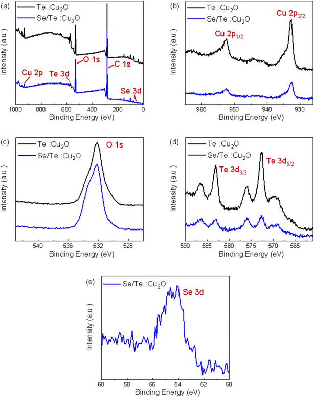 | ||
Fig. 5 The XPS spectra of Te![[thin space (1/6-em)]](https://www.rsc.org/images/entities/char_2009.gif) : :![[thin space (1/6-em)]](https://www.rsc.org/images/entities/char_2009.gif) Cu2O and Se/Te Cu2O and Se/Te![[thin space (1/6-em)]](https://www.rsc.org/images/entities/char_2009.gif) : :![[thin space (1/6-em)]](https://www.rsc.org/images/entities/char_2009.gif) Cu2O powders: (a) full spectra, (b) Cu 2p, (c) O 1s, (d) Te 3d, and (e) Se 3d. Cu2O powders: (a) full spectra, (b) Cu 2p, (c) O 1s, (d) Te 3d, and (e) Se 3d. | ||
Fig. 6 shows the EDS spectra of the Te![[thin space (1/6-em)]](https://www.rsc.org/images/entities/char_2009.gif) :
:![[thin space (1/6-em)]](https://www.rsc.org/images/entities/char_2009.gif) Cu2O and Se/Te
Cu2O and Se/Te![[thin space (1/6-em)]](https://www.rsc.org/images/entities/char_2009.gif) :
:![[thin space (1/6-em)]](https://www.rsc.org/images/entities/char_2009.gif) Cu2O thin films. It can be seen that the proportion of Te in Te
Cu2O thin films. It can be seen that the proportion of Te in Te![[thin space (1/6-em)]](https://www.rsc.org/images/entities/char_2009.gif) :
:![[thin space (1/6-em)]](https://www.rsc.org/images/entities/char_2009.gif) Cu2O was roughly the same as that in the experimental scheme, and basically it has been doped into Cu2O. The proportion of Se and Te in Se/Te
Cu2O was roughly the same as that in the experimental scheme, and basically it has been doped into Cu2O. The proportion of Se and Te in Se/Te![[thin space (1/6-em)]](https://www.rsc.org/images/entities/char_2009.gif) :
:![[thin space (1/6-em)]](https://www.rsc.org/images/entities/char_2009.gif) Cu2O was very small, about 1%, which was very different from the that found in the experimental scheme. As in the previous analysis, due to the same group elements competing and the large atomic radius difference, it was difficult to dope them into Cu2O. Nevertheless, the results of the XRD, XPS and EDS analyses confirmed that the Se and Te were doped into the Cu2O.
Cu2O was very small, about 1%, which was very different from the that found in the experimental scheme. As in the previous analysis, due to the same group elements competing and the large atomic radius difference, it was difficult to dope them into Cu2O. Nevertheless, the results of the XRD, XPS and EDS analyses confirmed that the Se and Te were doped into the Cu2O.
![[thin space (1/6-em)]](https://www.rsc.org/images/entities/char_2009.gif) :
:![[thin space (1/6-em)]](https://www.rsc.org/images/entities/char_2009.gif) Cu2O and Se/Te
Cu2O and Se/Te![[thin space (1/6-em)]](https://www.rsc.org/images/entities/char_2009.gif) :
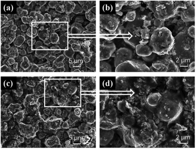
:![[thin space (1/6-em)]](https://www.rsc.org/images/entities/char_2009.gif) Cu2O thin films at a scale of 5 μm and 2 μm, respectively. The surface of the thin films prepared by this method show irregularly arranged lumpy particles of different sizes, with many small particles attached to the larger ones, and a very rough surface. The particles of the Te
Cu2O thin films at a scale of 5 μm and 2 μm, respectively. The surface of the thin films prepared by this method show irregularly arranged lumpy particles of different sizes, with many small particles attached to the larger ones, and a very rough surface. The particles of the Te![[thin space (1/6-em)]](https://www.rsc.org/images/entities/char_2009.gif) :
:![[thin space (1/6-em)]](https://www.rsc.org/images/entities/char_2009.gif) Cu2O were more independently distributed than Se/Te
Cu2O were more independently distributed than Se/Te![[thin space (1/6-em)]](https://www.rsc.org/images/entities/char_2009.gif) :
:![[thin space (1/6-em)]](https://www.rsc.org/images/entities/char_2009.gif) Cu2O, resembling the cubic structure of Cu2O.
Cu2O, resembling the cubic structure of Cu2O.
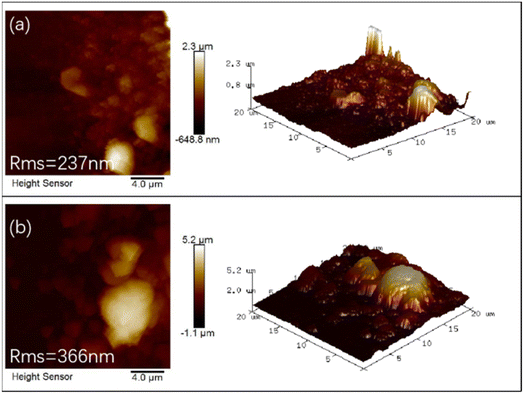
Fig. 8 shows the two-dimensional surface and the corresponding three-dimensional AFM images of the Te![[thin space (1/6-em)]](https://www.rsc.org/images/entities/char_2009.gif) :
:![[thin space (1/6-em)]](https://www.rsc.org/images/entities/char_2009.gif) Cu2O and Se/Te
Cu2O and Se/Te![[thin space (1/6-em)]](https://www.rsc.org/images/entities/char_2009.gif) :
:![[thin space (1/6-em)]](https://www.rsc.org/images/entities/char_2009.gif) Cu2O thin films. The surface particles of the two thin films were different in size and irregularly distributed, with agglomerated large particles, which were caused by solidification during sintering and cooling. The root mean square (Rms) of roughness of the Te
Cu2O thin films. The surface particles of the two thin films were different in size and irregularly distributed, with agglomerated large particles, which were caused by solidification during sintering and cooling. The root mean square (Rms) of roughness of the Te![[thin space (1/6-em)]](https://www.rsc.org/images/entities/char_2009.gif) :
:![[thin space (1/6-em)]](https://www.rsc.org/images/entities/char_2009.gif) Cu2O and Se/Te
Cu2O and Se/Te![[thin space (1/6-em)]](https://www.rsc.org/images/entities/char_2009.gif) :
:![[thin space (1/6-em)]](https://www.rsc.org/images/entities/char_2009.gif) Cu2O thin films were 237 nm and 366 nm, respectively. The thicknesses were 2.3 μm and 5.2 μm, respectively. The two thin films were compounded with the FTO substrate, with varying degrees of voids and poor thin film quality.
Cu2O thin films were 237 nm and 366 nm, respectively. The thicknesses were 2.3 μm and 5.2 μm, respectively. The two thin films were compounded with the FTO substrate, with varying degrees of voids and poor thin film quality.
Fig. 9 shows the results of the contact angle (CA) analysis of the three thin films. The average CAs of the three systems were 104.32°, 115.15° and 84.848° for 3 μL deionized water, whereas the CA of spiro-OMeTAD was only 67.1°.25 In contrast, both Cu2O and Cu2O doped thin films had better hydrophobic properties and better device stability.
 | ||
Fig. 9 Contact angles of (a) the Cu2O thin film, (b) the Te![[thin space (1/6-em)]](https://www.rsc.org/images/entities/char_2009.gif) : :![[thin space (1/6-em)]](https://www.rsc.org/images/entities/char_2009.gif) Cu2O thin film, and (c) the Se/Te Cu2O thin film, and (c) the Se/Te![[thin space (1/6-em)]](https://www.rsc.org/images/entities/char_2009.gif) : :![[thin space (1/6-em)]](https://www.rsc.org/images/entities/char_2009.gif) Cu2O thin film. Cu2O thin film. | ||
Table 5 shows the characterization parameters of the Hall effect for the three thin films at a temperature of 300 K, where the data of pure Cu2O are from the literature.26 The resistivity (R) was influenced by both carrier mobility and concentration, and at 300 K, the doped systems had a lower resistivity, higher carrier mobility and higher carrier concentration than the pure Cu2O. The high carrier mobility was produced because of a significant reduction in the effective mass, and was consistent with the results of the analysis of the increase of charge amount due to the emergence of free electrons after doping in the theoretical research, which improved the conductivity of the material.
![[thin space (1/6-em)]](https://www.rsc.org/images/entities/char_2009.gif) :
:![[thin space (1/6-em)]](https://www.rsc.org/images/entities/char_2009.gif) Cu2O and Se/Te
Cu2O and Se/Te![[thin space (1/6-em)]](https://www.rsc.org/images/entities/char_2009.gif) :
:![[thin space (1/6-em)]](https://www.rsc.org/images/entities/char_2009.gif) Cu2O thin films
Cu2O thin films
| R (Ω cm) | Mobility (cm2 V−1 s−1) | Concentration (cm−3) | |
|---|---|---|---|
| Cu2O | 1.35 × 10⁻³ | 60 | 2.0 × 10¹⁶ |
Te![[thin space (1/6-em)]](https://www.rsc.org/images/entities/char_2009.gif) : :![[thin space (1/6-em)]](https://www.rsc.org/images/entities/char_2009.gif) Cu2O Cu2O |
3.34 × 10⁻⁴ | 1052 | 1.78 × 10¹⁹ |
Se/Te![[thin space (1/6-em)]](https://www.rsc.org/images/entities/char_2009.gif) : :![[thin space (1/6-em)]](https://www.rsc.org/images/entities/char_2009.gif) Cu2O Cu2O |
4.13 × 10⁻⁴ | 1297 | 1.17 × 10¹⁹ |
![[thin space (1/6-em)]](https://www.rsc.org/images/entities/char_2009.gif) :
:![[thin space (1/6-em)]](https://www.rsc.org/images/entities/char_2009.gif) Cu2O and Se/Te
Cu2O and Se/Te![[thin space (1/6-em)]](https://www.rsc.org/images/entities/char_2009.gif) :
:![[thin space (1/6-em)]](https://www.rsc.org/images/entities/char_2009.gif) Cu2O had better absorbance than that of pure Cu2O, which was still about 0.95 at 800 nm. The bandgap values of 2.05 eV, 1.8 eV and 1.88 eV for the three films, were obtained from the Tauc plot relationship (Fig. 10(b)), corresponding to the colors of dark-red, black and silver-black, respectively. Considering the doping amount, the experimental bandgap value was in agreement with the expected results.
Cu2O had better absorbance than that of pure Cu2O, which was still about 0.95 at 800 nm. The bandgap values of 2.05 eV, 1.8 eV and 1.88 eV for the three films, were obtained from the Tauc plot relationship (Fig. 10(b)), corresponding to the colors of dark-red, black and silver-black, respectively. Considering the doping amount, the experimental bandgap value was in agreement with the expected results.
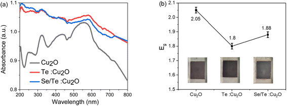 | ||
| Fig. 10 The UV-vis analysis results of three thin films: (a) absorption spectrum and (b) the corresponding Tauc curves. | ||
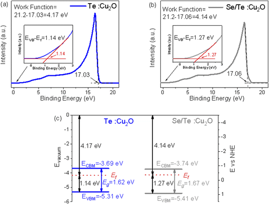
Fig. 11(a) and (b) show the ultraviolet photoelectron spectroscopy (UPS) of the Te![[thin space (1/6-em)]](https://www.rsc.org/images/entities/char_2009.gif) :
:![[thin space (1/6-em)]](https://www.rsc.org/images/entities/char_2009.gif) Cu2O and Se/Te
Cu2O and Se/Te![[thin space (1/6-em)]](https://www.rsc.org/images/entities/char_2009.gif) :
:![[thin space (1/6-em)]](https://www.rsc.org/images/entities/char_2009.gif) Cu2O thin films, and their Fermi level positions and the relative positions of the valence band edges were fitted. The Fermi level position was the excitation energy of the He–I spectrum (21.2 eV) minus the second ionization potential, and the relative position of the valence band edges was the first ionization potential value.27,28 In order to determine the energy level position of the doped systems more intuitively and effectively, Fig. 11(c) was drawn in combination with the bandgap energy level. It can be seen that both Te
Cu2O thin films, and their Fermi level positions and the relative positions of the valence band edges were fitted. The Fermi level position was the excitation energy of the He–I spectrum (21.2 eV) minus the second ionization potential, and the relative position of the valence band edges was the first ionization potential value.27,28 In order to determine the energy level position of the doped systems more intuitively and effectively, Fig. 11(c) was drawn in combination with the bandgap energy level. It can be seen that both Te![[thin space (1/6-em)]](https://www.rsc.org/images/entities/char_2009.gif) :
:![[thin space (1/6-em)]](https://www.rsc.org/images/entities/char_2009.gif) Cu2O and Se/Te
Cu2O and Se/Te![[thin space (1/6-em)]](https://www.rsc.org/images/entities/char_2009.gif) :
:![[thin space (1/6-em)]](https://www.rsc.org/images/entities/char_2009.gif) Cu2O have good energy level matching with the MAPbI3 (EVBM = −5.5 eV, ECBM = −3.9 eV) to make efficient transport holes and block electrons.
Cu2O have good energy level matching with the MAPbI3 (EVBM = −5.5 eV, ECBM = −3.9 eV) to make efficient transport holes and block electrons.
4 Solar cell simulation
4.1 Model and parameters
Firstly, a PSC model of FTO/TiO2/IDL1/MAPbI3/IDL2/spiro-OMeTAD/Au was established, and modeled by substituting different HTLs, where IDL1 and IDL2 have interfaced defect layers. Then, the parameters of each layer of the cell were set, as shown in Table 6. The parameters for Cu2O and spiro-OMeTAD were all found from reports in the literature,29–32 the parameters of Te![[thin space (1/6-em)]](https://www.rsc.org/images/entities/char_2009.gif) :
:![[thin space (1/6-em)]](https://www.rsc.org/images/entities/char_2009.gif) Cu2O and Se/Te
Cu2O and Se/Te![[thin space (1/6-em)]](https://www.rsc.org/images/entities/char_2009.gif) :
:![[thin space (1/6-em)]](https://www.rsc.org/images/entities/char_2009.gif) Cu2O were mainly from the experimental research, with some using the parameters of Cu2O. The work function of Au was 5.1 eV. Finally, the simulation was carried out under a temperature of 300 K, standard sunlight AM1.5 G illumination intensity, and the series-parallel resistance was ignored.
Cu2O were mainly from the experimental research, with some using the parameters of Cu2O. The work function of Au was 5.1 eV. Finally, the simulation was carried out under a temperature of 300 K, standard sunlight AM1.5 G illumination intensity, and the series-parallel resistance was ignored.
| Spiro-OMeTAD | Cu2O | Te![[thin space (1/6-em)]](https://www.rsc.org/images/entities/char_2009.gif) : :![[thin space (1/6-em)]](https://www.rsc.org/images/entities/char_2009.gif) Cu2O Cu2O |
Se/Te![[thin space (1/6-em)]](https://www.rsc.org/images/entities/char_2009.gif) : :![[thin space (1/6-em)]](https://www.rsc.org/images/entities/char_2009.gif) Cu2O Cu2O |
MAPbI3 | IDL1/2 | TiO2 | |
|---|---|---|---|---|---|---|---|
| Thickness (nm) | 400 | 400 | 400 | 400 | 450 | 10 | 50 |
| Eg (eV) | 3.17 | 2.05 | 1.8 | 1.88 | 1.55 | 1.55 | 3.2 |
| χ (eV) | 2.05 | 3.2 | 3.51 | 3.53 | 3.93 | 3.93 | 4.26 |
| εr | 3.0 | 7.11 | 7.11 | 7.11 | 6.5 | 6.5 | 9 |
| Nc (cm−3) | 2.2 × 10¹⁸ | 2 × 10¹⁷ | 2 × 10¹⁷ | 2 × 10¹⁷ | 2.2 × 10¹⁸ | 2.2 × 10¹⁸ | 1 × 10²¹ |
| Nv (cm−3) | 1.8 × 10¹⁹ | 1.1 × 10¹⁹ | 1.78 × 10¹⁹ | 1.17 × 10¹⁹ | 1.8 × 10¹⁹ | 1.8 × 10¹⁹ | 2 × 10²⁰ |
| μn (cm2 V−1 s−1) | 2 × 10⁻⁴ | 80 | 1052 | 1297 | 2 | 2 | 20 |
| μp (cm2 V−1 s−1) | 2 × 10⁻⁴ | 80 | 1052 | 1297 | 2 | 2 | 10 |
| ND (cm−3) | 0 | 0 | 0 | 0 | 1 × 10¹³ | 1 × 10¹³ | 5 × 10¹⁹ |
| NA (cm−3) | 2 × 10¹⁹ | 3 × 10¹⁸ | 3 × 10¹⁸ | 3 × 10¹⁸ | 0 | 0 | 0 |
| Nt (cm−3) | 1 × 10¹⁵ | 1 × 10¹⁵ | 1 × 10¹⁵ | 1 × 10¹⁵ | 2.5 × 10¹³ | 1 × 10¹⁷ | 1 × 10¹⁵ |
4.2 Numerical calculation results and discussion
![[thin space (1/6-em)]](https://www.rsc.org/images/entities/char_2009.gif) :
:![[thin space (1/6-em)]](https://www.rsc.org/images/entities/char_2009.gif) Cu2O-based PSC showing the best performance parameters. The doped Cu2O-based PSCs had an improved Jsc when compared to that of Cu2O-based PSC due to the improved carrier mobility enhancement.
Cu2O-based PSC showing the best performance parameters. The doped Cu2O-based PSCs had an improved Jsc when compared to that of Cu2O-based PSC due to the improved carrier mobility enhancement.
| Voc (V) | Jsc (mA cm−2) | FF (%) | PCE (%) | |
|---|---|---|---|---|
| Spiro-OMeTAD | 1.06 | 23.20 | 74.96 | 18.47 |
| Cu2O | 1.06 | 23.36 | 74.46 | 18.43 |
Te![[thin space (1/6-em)]](https://www.rsc.org/images/entities/char_2009.gif) : :![[thin space (1/6-em)]](https://www.rsc.org/images/entities/char_2009.gif) Cu2O Cu2O |
1.08 | 23.60 | 77.69 | 19.96 |
Se/Te![[thin space (1/6-em)]](https://www.rsc.org/images/entities/char_2009.gif) : :![[thin space (1/6-em)]](https://www.rsc.org/images/entities/char_2009.gif) Cu2O Cu2O |
1.16 | 23.51 | 82.47 | 22.42 |
![[thin space (1/6-em)]](https://www.rsc.org/images/entities/char_2009.gif) :
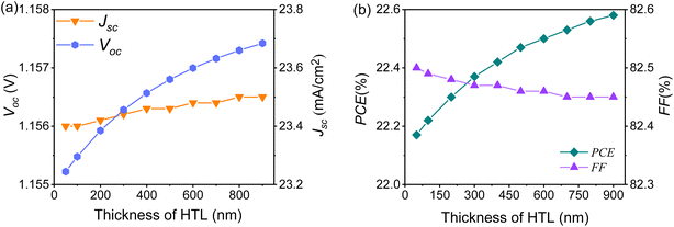
:![[thin space (1/6-em)]](https://www.rsc.org/images/entities/char_2009.gif) Cu2O thin film from 50 nm, to 100 nm to 900 nm (at 100 nm intervals), and the final results were calculated, and are shown in Fig. 12. It can be seen that the values of Voc, Jsc and PCE were on an upward trend with the increase of film thickness, and the increase rate became slow. The fill factor (FF) at 50 nm was 82.5%, after which it started to decrease with the increasing thin film thickness and changed little after 600 nm. Because the Cu2O thin film is a thickness-insensitive material,33 the low proportion of Se/Te doping may have a minor effect on the film formation, so the Se/Te
Cu2O thin film from 50 nm, to 100 nm to 900 nm (at 100 nm intervals), and the final results were calculated, and are shown in Fig. 12. It can be seen that the values of Voc, Jsc and PCE were on an upward trend with the increase of film thickness, and the increase rate became slow. The fill factor (FF) at 50 nm was 82.5%, after which it started to decrease with the increasing thin film thickness and changed little after 600 nm. Because the Cu2O thin film is a thickness-insensitive material,33 the low proportion of Se/Te doping may have a minor effect on the film formation, so the Se/Te![[thin space (1/6-em)]](https://www.rsc.org/images/entities/char_2009.gif) :
:![[thin space (1/6-em)]](https://www.rsc.org/images/entities/char_2009.gif) Cu2O thin films at different thicknesses had a minor effect on the performance parameters of the PSCs.
Cu2O thin films at different thicknesses had a minor effect on the performance parameters of the PSCs.
![[thin space (1/6-em)]](https://www.rsc.org/images/entities/char_2009.gif) :
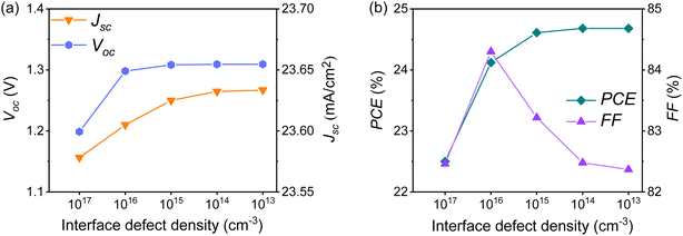
:![[thin space (1/6-em)]](https://www.rsc.org/images/entities/char_2009.gif) Cu2O-based PSC, with a thickness of 600 nm, its IDL density was changed to explore the effect on the performance of solar cells. Setting the density in the range of 1013 cm−3 to 1017 cm−3, the final calculated result is shown in Fig. 13. It can be seen when the IDL density was lower than 1014 cm−3, the solar cell's performance reached an optimal stable state, where Voc is 1.26 V, Jsc is 23.65 mA cm−2, FF is 82.48%, and the PCE is up to 24.68%.
Cu2O-based PSC, with a thickness of 600 nm, its IDL density was changed to explore the effect on the performance of solar cells. Setting the density in the range of 1013 cm−3 to 1017 cm−3, the final calculated result is shown in Fig. 13. It can be seen when the IDL density was lower than 1014 cm−3, the solar cell's performance reached an optimal stable state, where Voc is 1.26 V, Jsc is 23.65 mA cm−2, FF is 82.48%, and the PCE is up to 24.68%.
5 Conclusions
(1) The theoretical construction of the Te![[thin space (1/6-em)]](https://www.rsc.org/images/entities/char_2009.gif) :
:![[thin space (1/6-em)]](https://www.rsc.org/images/entities/char_2009.gif) Cu2O and Se/Te
Cu2O and Se/Te![[thin space (1/6-em)]](https://www.rsc.org/images/entities/char_2009.gif) :
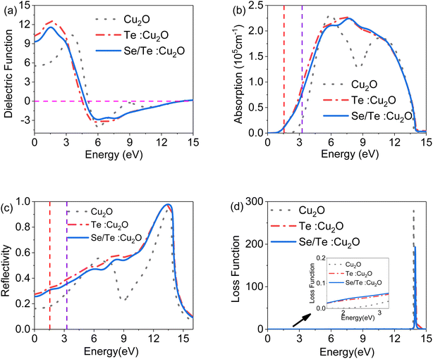
:![[thin space (1/6-em)]](https://www.rsc.org/images/entities/char_2009.gif) Cu2O models with a 12.5% doping ratio showed a lattice distortion after geometrical optimization, and the bandgaps were 1.489 eV and 1.545 eV, respectively, and the conductivity, absorption coefficient and reflectivity were all improved.
Cu2O models with a 12.5% doping ratio showed a lattice distortion after geometrical optimization, and the bandgaps were 1.489 eV and 1.545 eV, respectively, and the conductivity, absorption coefficient and reflectivity were all improved.
(2) The Te![[thin space (1/6-em)]](https://www.rsc.org/images/entities/char_2009.gif) :
:![[thin space (1/6-em)]](https://www.rsc.org/images/entities/char_2009.gif) Cu2O and Se/Te
Cu2O and Se/Te![[thin space (1/6-em)]](https://www.rsc.org/images/entities/char_2009.gif) :
:![[thin space (1/6-em)]](https://www.rsc.org/images/entities/char_2009.gif) Cu2O with doping ratios of 7.4% and 10.71%, respectively, were prepared experimentally. The doping of Se and Te into Cu2O was confirmed by the results of XRD, XPS and EDS analysis, and all three thin films had good stability as determined by contact angle analysis, and the improved conductivity of both thin films as determined by the Hall analysis, and both thin films had a good energy level match when comparing with the MAPbI3 properties obtained using UV-vis and UPS analyses. The electrical and optical properties of the Se/Te
Cu2O with doping ratios of 7.4% and 10.71%, respectively, were prepared experimentally. The doping of Se and Te into Cu2O was confirmed by the results of XRD, XPS and EDS analysis, and all three thin films had good stability as determined by contact angle analysis, and the improved conductivity of both thin films as determined by the Hall analysis, and both thin films had a good energy level match when comparing with the MAPbI3 properties obtained using UV-vis and UPS analyses. The electrical and optical properties of the Se/Te![[thin space (1/6-em)]](https://www.rsc.org/images/entities/char_2009.gif) :
:![[thin space (1/6-em)]](https://www.rsc.org/images/entities/char_2009.gif) Cu2O thin film were relatively better than the others, which was beneficial for their use as HTL.
Cu2O thin film were relatively better than the others, which was beneficial for their use as HTL.
(3) Solar cells with four different HTLs were simulated, and the Se/Te![[thin space (1/6-em)]](https://www.rsc.org/images/entities/char_2009.gif) :
:![[thin space (1/6-em)]](https://www.rsc.org/images/entities/char_2009.gif) Cu2O-based PSC showed the best performance. After optimization, with the thickness of Se/Te
Cu2O-based PSC showed the best performance. After optimization, with the thickness of Se/Te![[thin space (1/6-em)]](https://www.rsc.org/images/entities/char_2009.gif) :
:![[thin space (1/6-em)]](https://www.rsc.org/images/entities/char_2009.gif) Cu2O at 600 nm, and the IDL density at 1014 cm−3, the PCE of the PSCs could reach 24.68%. Compared with the PCE of Cu2O-based PSC, it has increased by 34%.
Cu2O at 600 nm, and the IDL density at 1014 cm−3, the PCE of the PSCs could reach 24.68%. Compared with the PCE of Cu2O-based PSC, it has increased by 34%.
6 Theoretical and experimental details
6.1 First-principles calculation
Calculations were made using the CASTEP module in the BIOVIA Materials Studio software. The exchange-correlation energy was determined by the GGA-PBEsol method. The valence electrons of the atoms were described by the ultrasoft pseudopotential, in which the proportions were set as Cu 3d104s1, O 2s22p4, Se 4s24p4, and Te 5s25p4. The electron wave function was expanded in the plane-wave basis set with a cutoff energy of 440 eV, and a Monkhorst–Pack grid with parameters of a 6 × 3 × 3 k-point was used for irreducible Brillouin zone sampling. All the atoms were optimized geometrically by using the Broyden-Fletcher-Goldfarb-Shanno (BFGS) method.6.2 Effective mass calculation
The effective mass of the electrons and holes in the unit of free-electron mass (m0) was estimated by fitting the energy-momentum dependence of the states at the CBM and VBM in the Brillouin zone. Electron effective mass was calculated at the CBM, and hole effective mass at the VBM near the G point in G-F direction, and in the [111] direction.6.3 Powder preparation
Cu2O, Te and Se powders of 99.99% purity were weighed, respectively. The powders were placed into a high-temperature tube furnace with a nitrogen atmosphere for sintering. The melting points of Se and Te were 217 °C and 452 °C, respectively, so they were sintered at 600 °C for 30 min.6.4 Ink preparation
The Cu2O powder (225 mg), Te![[thin space (1/6-em)]](https://www.rsc.org/images/entities/char_2009.gif) :
:![[thin space (1/6-em)]](https://www.rsc.org/images/entities/char_2009.gif) Cu2O powder (230 mg), and Se/Te
Cu2O powder (230 mg), and Se/Te![[thin space (1/6-em)]](https://www.rsc.org/images/entities/char_2009.gif) :
:![[thin space (1/6-em)]](https://www.rsc.org/images/entities/char_2009.gif) Cu2O powder (270 mg) were weighed into centrifuge tubes, and 50 μL of deionized water was added to each one. Each solution was mixed ultrasonically for 40 min, and then 30 μL of ethanolamine was added followed by ultrasonic mixing for a further 40 min.
Cu2O powder (270 mg) were weighed into centrifuge tubes, and 50 μL of deionized water was added to each one. Each solution was mixed ultrasonically for 40 min, and then 30 μL of ethanolamine was added followed by ultrasonic mixing for a further 40 min.
6.5 Thin film preparation
The FTOs were placed into a beaker and mixed ultrasonically for 10 min with acetone, absolute ethanol and deionized water, then dried with nitrogen, and then irradiated with UV light for 3 min, for the conversion to a thin film substrate. Then, 10 μL of ink was drop-coated onto the FTO conductive glass surface. The three thin films were prepared by spin-coating at 1200 rpm, 1800 rpm and 1500 rpm for 15 s. The film was placed on a graphite heating plate, heated at 80 °C for 15 min and baked until semi-dried. The film was trimmed into a 10 × 8 mm shape, and then placed on a graphite heating plate, and heated at 130 °C for 15 min and then baked. Lastly, the thin film was put into a high-temperature tube furnace with a nitrogen atmosphere and annealed at 200 °C for 60 min.Author contributions
L. Luo conceived the project, planned and carried out the simulations, performed the experiments and data analysis, and wrote the manuscript. B. Zhou conceived the project, planned and carried out the simulations, and wrote the manuscript. Y. Hu conceived the project. Q. Zhao planned and carried out the simulations. X. Yang planned and carried out the simulations. Z. Liu performed the experiments and data analysis. C. Wang performed the experiments and data analysis. Z. Duan performed the experiments and data analysis. Z. Xie performed the experiments and data analysis. All the authors edited and approved the manuscript.Conflicts of interest
The authors declare that they have no known financial interests or personal relationships that could appear to influence the work in this paper.Acknowledgements
This work was supported by Yunnan Provincial Science and Technology Department (202101BA070001-054). The authors wish to give special thanks to Dr Marc Burgelman, the developer of SCAPS, for his help with the SCAPS software.References
- Y. Jiang, H. Yuan and H. Chen, Phys. Chem. Chem. Phys., 2015, 17, 630–637 RSC
.
- R. Zhang, L. Ling, Z. Li and B. Wang, Appl. Catal., A, 2011, 400, 142–147 CrossRef CAS
.
- M. Su, Z. Liang, C. Zhao, P. Liu, S. Yue and W. Xie, Mater. Lett., 2016, 170, 80–84 CrossRef CAS
.
- G. A. Casas, M. A. Cappelletti, A. P. Cédola, B. M. Soucase and E. L. Peltzer y Blancá, Superlattices Microstruct., 2017, 107, 136–143 CrossRef CAS
.
- A. M. Elseman, M. S. Selim, L. Luo, C. Y. Xu, G. Wang, Y. Jiang, B. Liu, L. P. Liao, Z. Hao and Q. L. Song, ChemSusChem, 2019, 12, 3808–3816 CrossRef CAS
.
- M. A. Islam, Y. A. Wahab, M. U. Khandaker, A. Alsubaie, A. S. A. Almalki, D. A. Bradley and N. Amin, Crystals, 2021, 11, 389 CrossRef CAS
.
- H. Rao, S. Ye, W. Sun, W. Yan, Y. Li, H. Peng, Z. Liu, Z. Bian, Y. Li and C. Huang, Nano Energy, 2016, 27, 51–57 CrossRef CAS
.
- C.-C. Tseng, L.-C. Chen, L.-B. Chang, G.-M. Wu, W.-S. Feng, M.-J. Jeng, D.-W. Chen and K.-L. Lee, J. Sol. Energy, 2020, 204, 270–279 CrossRef CAS
.
- C. Liu, X. Zhou, S. Chen, X. Zhao, S. Dai and B. Xu, Adv. Sci., 2019, 6, 1801169 CrossRef
.
- Z.-H. Lin, P. Roy, Z.-Y. Shih, C.-M. Ou and H.-T. Chang, ChemPlusChem, 2013, 78, 302–309 CrossRef CAS
.
- H. Güney and Ç. Duman, AIP Conf. Proc., 2016, 1726, 020122 CrossRef
.
- Y.-L. Liu, C.-L. Yang, M.-S. Wang, X.-G. Ma and Y.-G. Yi, Mater. Res. Bull., 2018, 107, 125–131 CrossRef CAS
.
- B. Zhou, L. Luo, Y. Zhang, Y. Hu, Z. Xie, Z. Duan and X. Yang, Mater. Res. Express., 2022, 9, 035902 CrossRef
.
- X. Ling, Z. Jin, Q. Jiang, X. Wang, B. Wei, Z. Wang, Y. Xu, T. Cao, J. W. Engle, W. Cai, C. Su and Q. He, Natl. Sci. Rev., 2021, 8, nwaa156 CrossRef CAS
.
- M. M. Obeid, Y. Mogulkoc, S. J. Edrees, Y. O. Ciftci, M. M. Shukur and M. M. H. Al-Marzooqee, Mater. Res. Bull., 2018, 108, 255–265 CrossRef CAS
.
- C. Zuo and L. Ding, Small, 2015, 11, 5528–5532 CrossRef CAS PubMed
.
- X. Zhang, X. Cui, Y. Sun, K. Qi, Z. Jin, S. Wei, W. Li, L. Zhang and W. Zheng, ACS Appl. Mater. Interfaces, 2018, 10, 745–752 CrossRef CAS PubMed
.
- X.-G. Yan, L. Xu, W.-Q. Huang, G.-F. Huang, Z.-M. Yang, S. Q. Zhan and J.-P. Long, Mater. Sci. Semicond. Process., 2014, 23, 34–41 CrossRef CAS
.
- D. Sharma, S. Upadhyay, V. R. Satsangi, R. Shrivastav, U. V. Waghmare and S. Dass, Appl. Catal., 2016, 18, 75–85 CrossRef
.
- J. Dong, K. Yang, B. Xu, L. Zhang, Q. Zhang and Y. Tian, J. Alloys Compd., 2015, 647, 295–302 CrossRef CAS
.
- X. Ye, G. Chen, B. Duan and P. Zhai, J. Electron. Mater., 2014, 44, 1674–1678 CrossRef
.
- M. Behera, R. Panda and R. Naik, Indian J. Phys., 2017, 91, 555–562 CrossRef CAS
.
- A. Saha, S. Payra, B. Selvaratnam, S. Bhattacharya, S. Pal, R. T. Koodali and S. Banerjee, ACS Sustainable Chem. Eng., 2018, 6, 11345–11352 CrossRef CAS
.
- D. Rajska, A. Brzózka, M. Marciszko-Wiąckowska, M. M. Marzec, D. Chlebda, K. E. Hnida-Gut and G. D. Sulka, Appl. Surf. Sci., 2021, 537, 147715 CrossRef CAS
.
- V. M. Arivunithi, H.-Y. Park, S. S. Reddy, Y. Do, H. Park, E.-S. Shin, Y.-Y. Noh, M. Song and S.-H. Jin, Macromol. Res., 2021, 29, 149–156 CrossRef CAS
.
- S. Ishizuka, S. Kato, Y. Okamoto, T. Sakurai, K. Akimoto, N. Fujiwara and H. Kobayashi, Appl. Surf. Sci., 2003, 216, 94–97 CrossRef CAS
.
- Y. S. Kwon, J. Lim, H. J. Yun, Y. H. Kim and T. Park, Energy Environ. Sci., 2014, 7, 1454–1460 RSC
.
- Y. Yao, B.-P. Zhang, J. Pei, Y.-C. Liu and J.-F. Li, J. Mater. Chem. C, 2017, 5, 7845–7852 RSC
.
- K. R. Adhikari, S. Gurung, B. K. Bhattarai and B. M. Soucase, Phys. Status Solidi C, 2016, 13, 13–17 CrossRef CAS
.
- F. Azri, A. Meftah, N. Sengouga and A. Meftah, J. Sol. Energy, 2019, 181, 372–378 CrossRef CAS
.
- L. Huang, X. Sun, C. Li, R. Xu, J. Xu, Y. Du, Y. Wu, J. Ni, H. Cai, J. Li, Z. Hu and J. Zhang, Sol. Energy Mater. Sol. Cells, 2016, 157, 1038–1047 CrossRef CAS
.
- L. Lin, P. Li, L. Jiang, Z. Kang, Q. Yan, H. Xiong, S. Lien, P. Zhang and Y. Qiu, J. Sol. Energy, 2021, 215, 328–334 CrossRef CAS
.
- S. Maryam, N. Mufti, A. Fuad, Y. A. S. Laksono, A. Taufiq and Sunaryono, IOP Conf. Ser.: Earth Environ. Sci., 2019, 276, 012035 CrossRef
.
| This journal is © The Royal Society of Chemistry 2023 |


