 Open Access Article
Creative Commons Attribution 3.0 Unported Licence
Infrared sensitive mixed phase of V7O16 and V2O5 thin-films†
Anchal Ranaa,
Aditya Yadavb,
Govind Gupta b and
Abhimanyu Rana
 *a
*a
aCentre for Advanced Materials and Devices, School of Engineering and Technology, BML Munjal University, Sidhrawali, Gurugram-122413, Haryana, India. E-mail: rana.abhimanyu@gmail.com
bCSIR-National Physical Laboratory, K. S. Krishnan Marg, New Delhi, 110012, India
First published on 22nd May 2023
Abstract
We report an infrared (IR) sensitive mixed phase of V7O16 and V2O5 thin films, grown by cathodic vacuum arc-deposition on glass substrates at relatively low temperatures. We have found that the mixed phase of V7O16 and V2O5 can be stabilized by post-annealing of amorphous VxOy between 300–400 °C, which gets fully converted into V2O5 after annealing at higher temperatures ∼450 °C. The local conversion from VxOy to V2O5 has also been demonstrated by applying different laser powers in Raman spectroscopy measurements. The optical transmission of these films increases as the content of V2O5 increases but the electrical conductivity and the optical bandgap decrease. These results are explained by the role of defects (oxygen vacancies) through the photoluminescence (PL) and time-resolved photoluminescence (TRPL) measurements. The IR sensitivity of the mixed phase is explained by the plasmonic absorption by the V7O16 degenerate semiconductor.
Introduction
Infrared (IR) sensitive materials have been of significant interest for IR sensors and smart windows in which the resistance or the optical transmission can be modulated by heating or IR radiation.1,2 Therefore, many low-bandgap semiconductors,3,4 quantum-well heterostructures5 and high-temperature-superconductors6,7 are intensively studied. However, these materials need to be cooled at lower temperatures for these applications. Vanadium-based oxides, found in more than 52 stable and metastable phases, have been investigated for developing uncooled devices as they show metal–insulator transitions (MIT) close to room temperatures under different external stimuli such as thermal, electrical, and optical.8–14 Vanadium (V) can have oxidation states varying from +2 to +5, where V2O3, VO2, and V2O5 are the most studied phases but other non-stoichiometric phases such as V3O7, V4O9, V6O13, V7O16 have also been reported, that occur due to the presence of more than one valency of V atom in a single crystal structure.14–17 Although, VO2 (having V4+ valency) has been the most preferred phase for IR sensors10,11,18 and smart windows due to sharp MIT close to room temperature,19–22 it has limitations of growing in the right phase on arbitrary substrates at low temperatures. On the other hand, V2O5 having a layered structure is important for energy storage electrodes,23–26 gas sensors27–29 and chromogenic applications.30–32 However, the applicability of the pure V2O5 phase is again largely restricted due to high temperature growth and poor electrical conductivity. The mixed phase of VO2 and V2O5 has been reported to give enhanced IR sensitivity.33 Other phases such as V7O16 could be promising for these applications which has the mixture of both V4+ and V5+ arranged in a layered crystal structure.15,34,35 However, there are very few reports on V7O16 phase which has been reported during chemical synthesis of V2O5 nanotubes28,35 or in thin film form when grown under oxygen deficient conditions using pulsed laser deposition29 and atomic layer deposition.15 There is a clear research gap for in-depth understanding of electronic and optical properties of V7O16 for any practical application in smart windows and IR sensors. Here, we systematically tune the contents of V7O16 and V2O5 in a mixed phase (also changing the V4+ and V5+ ratio) by post-annealing of amorphous vanadium oxide thin films grown by cathodic vacuum arc-deposition. We report a strong modulation of electrical resistance and optical transmission in these films with IR radiation and temperature.Materials and methods
First an amorphous vanadium oxide thin films were grown on high-grade barium-borosilicate 7059 glass substrates using cathodic vacuum arc-deposition by evaporating a vanadium metal target (∼99.99% purity) in the presence of oxygen at a partial pressure of ∼1 × 10⁻³ mbar, arc current of ∼150 A, substrate temperature ∼200 °C and substrate bias of −60 V. These films were then taken out and annealed in air at different temperatures i.e., ∼300 °C, ∼350 °C, ∼400 °C, ∼450 °C, and 520 °C for 2 hours. The unannealed sample will be called as Sas-grown and other annealed sampled as S300, S350, S400, S450, and S520 in this manuscript. The Raman spectroscopy was carried out using a commercial spectrometer by WiTech (Alpha 300) having a green laser of 532 nm wavelength. The crystal structure was confirmed by X-ray diffraction (XRD, Panalytical Empyrean Model) by scanning 2θ ranging from 10° to 90° at a step size of 0.02° using Cu Kα radiation (λ ∼ 1.54 Å). The X-ray photoelectron spectroscopy (XPS) was carried out using XPS/ESCA, K-ALPHA+, Thermo Fisher Scientific. The deconvolution and fitting of XPS data of was performed using XPSpeak41 software. The optical transmission spectra were obtained in the wavelength range from 380 nm to 800 nm using a UV-visible spectrometer by PerkinElmer LAMBDA 365 model. Electrical measurements were performed using a four-probe setup equipped with Keithley electrometers. The IR sensing measurements were carried out using the IR source by Newport model 6363IR having intensity ∼438 W m−2. Photoluminescence (PL) and time-resolved photoluminescence (TRPL) were recorded at the excitation wavelength of ∼350 nm and ∼266 nm (pulsed) using Edinburgh (FLS 980D2D2) set-up.Results and discussion
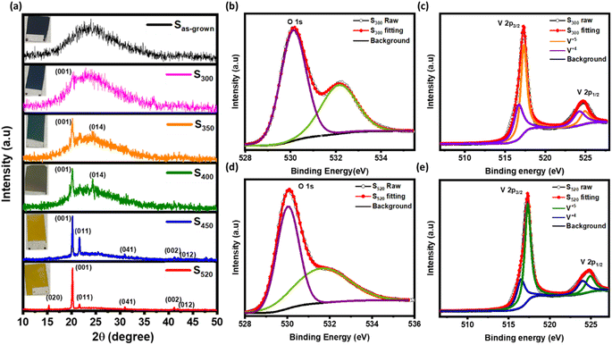
The XRD patterns of Sas-grown, S300, S350, S400, S450, and S520 are shown in Fig. 1(a) with their corresponding photographs in the inset. Apparently, the photographic images show a clear change in colour from black (of amorphous films) to the yellowish orange after annealing. There is also a clear transition in XRD spectra from a broad hump in Sas-grown to sharp peaks in annealed samples at ∼15.3°, ∼20.18°, ∼21.65°, ∼31.04°, ∼41.21° and ∼41.87° related to (020), (001), (011), (040), (002), and (012) crystalline planes of the pure orthorhombic phase of V2O5 respectively. However, the peak at ∼24.5° confirms the presence of the V7O16 triclinic phase15,34 in S350 and S400 samples.To further confirm the presence of V7O16, the X-ray photoelectron spectroscopy (XPS) were performed on S300 and S520, as shown in Fig. 1(b, c) and (d, e) respectively. The binding energy peak ∼284.8 eV of carbon 1s orbital was used to compensate the shifts in other peaks due to charging. The XPS spectra for 2p orbitals of vanadium (V) has two peaks corresponding to 2p3/2 and 2p1/2 due to the spin–orbit splitting of ∼7.5 eV. However, each peak 2p3/2 and 2p1/2 were further deconvoluted that correspond to the presence of V4+ (∼516.5 eV & ∼524 eV) and V5+ (∼517.5 eV & ∼525 eV).15,36 The peak at ∼530 eV is related to 1s oxygen in vanadium oxygen bonds,37,38 but other peaks at higher energies ∼532 eV are due to free hydroxyl groups adsorbed on the hydrophilic surfaces.39 The ratio of V4+ and V5+ contents in S300 and S520, estimated by the dividing the area under the curve of respective peaks, is found to be consistent with literature,15,40 implying higher V4+ content in these samples having V7O16 phase. In S520, peaks corresponding to V4+ were observed because of the photoreduction of V5+ in V2O5 phase.41
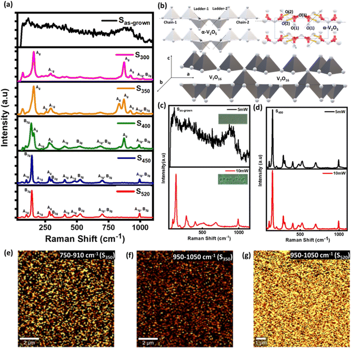
The Raman spectroscopic results of these films are compared in Fig. 2. Due to the amorphous nature of Sas-grown film, no sharp peaks were observed but as annealing temperature exceeds 300 °C, sharp peaks start appearing. The Raman spectra for S450 and S520 shows peaks at ∼101, ∼144, ∼194, ∼282, ∼304, ∼404, ∼483, ∼507, ∼528, ∼699, and ∼992 cm−1 due to different vibrational modes of V2O5 phase,14,15,42–44 as description given in Table 1. Especially, the strongest peak at ∼144 cm−1 arises from the V–O–V chains of the layered structure of α-V2O5, as shown in Fig. 2(b). For the samples annealed below 400 °C (S300 and S350), the peaks around ∼158, ∼255, ∼294, ∼832, ∼870, ∼970 cm−1 confirms the presence of V7O16 phase, also consistent with the earlier studies.14,44,45 It is to be noted that the presence of other polymorphs of V2O5 (β- γ-)14,26,42,44 cannot be completely ruled out using Raman spectroscopy due to overlapping peak positions.14 Fig. 2(b) shows the schematic of V7O16 phase where the layered structure resembles to α-V2O5, causing the peak ∼144 cm−1 to be shifted to higher wavenumber ∼158 cm−1. However, the other vibrational modes related to ladder steps (LS) seems to be missing in V7O16, indicating the absence of LS in this phase. Clearly, other peaks at ∼255, ∼294, ∼832, ∼870, and ∼970 cm−1 could be assigned to the vibrational modes of V![[double bond, length as m-dash]](https://www.rsc.org/images/entities/char_e001.gif) O bonds (Ag symmetry).15 Also, the Raman spectroscopy performed at different laser powers (5 mW to 10 mW) in Fig. 2(c) and (d) shows the immediate conversion of amorphous phase to V2O5, unlike the annealed samples. Similar conversion was also observed by other groups in case of chemically synthesized VOx nanotubes.43 This study opens further questions of stabilizing the intermediate phase of V7O16 using laser heating and open the opportunities for applications in laser writing for high security tags and detection Fig. 2(e)–(g) shows the Raman mapping of S350 and S520 samples. Since the Raman spectra of the S350 show the characteristic peaks at ∼832 cm−1, 870 cm−1, 920 cm−1 and S520 at 994 cm−1, we performed Raman mapping by selecting two wavelengths range from 750–910 cm−1 and 950–1050 cm−1 so that we could capture the regions of V7O16 and V2O5 spatially in 10 × 10 μm2 area. In Fig. 2(e) and (f), for S350 both V7O16 and V2O5 phases can be seen. On the other hand, for S520 the brighter region mostly cover the V2O5 with some minor black regions due to some other phases.
O bonds (Ag symmetry).15 Also, the Raman spectroscopy performed at different laser powers (5 mW to 10 mW) in Fig. 2(c) and (d) shows the immediate conversion of amorphous phase to V2O5, unlike the annealed samples. Similar conversion was also observed by other groups in case of chemically synthesized VOx nanotubes.43 This study opens further questions of stabilizing the intermediate phase of V7O16 using laser heating and open the opportunities for applications in laser writing for high security tags and detection Fig. 2(e)–(g) shows the Raman mapping of S350 and S520 samples. Since the Raman spectra of the S350 show the characteristic peaks at ∼832 cm−1, 870 cm−1, 920 cm−1 and S520 at 994 cm−1, we performed Raman mapping by selecting two wavelengths range from 750–910 cm−1 and 950–1050 cm−1 so that we could capture the regions of V7O16 and V2O5 spatially in 10 × 10 μm2 area. In Fig. 2(e) and (f), for S350 both V7O16 and V2O5 phases can be seen. On the other hand, for S520 the brighter region mostly cover the V2O5 with some minor black regions due to some other phases.
| ν (cm−1) | Description | Phonon modes |
|---|---|---|
| 101 | In phase rotation of the V2O4 ladder step (LS) unit in b-axis (crystalline V2O5)14,42 | A1g |
| 144 | Skeleton bending of V–O–V chain (crystalline V2O5)14 | B2g |
| 158 | Skeleton bending of V–O–V chain (crystalline V7O16)14,15 | Ag |
| 194 | Bending of O(2)–V–O(3) (crystalline V2O5)14 | A1g |
| 255 | Vibration of the V![[double bond, length as m-dash]](https://www.rsc.org/images/entities/char_e001.gif) O bond (crystalline V7O16) O bond (crystalline V7O16) |
Ag |
| 282 | Bending of V![[double bond, length as m-dash]](https://www.rsc.org/images/entities/char_e001.gif) O (crystalline V2O5)14 O (crystalline V2O5)14 |
A1g |
| 294 | Bending of V![[double bond, length as m-dash]](https://www.rsc.org/images/entities/char_e001.gif) O (crystalline V7O16) O (crystalline V7O16) |
Ag |
| 304 | Bending of V–O(2) (crystalline V2O5)14 | B2g |
| 404 | Angle-bending of V–O(3)–V bonds (crystalline V2O5)14 | A1g |
| 483 | Symmetric stretching of V–O(3)–V bonds (crystalline V2O5)14 | A1g |
| 507 | Stretching vibrations of V–O(2) bonds (crystalline V2O5)14 | B2g |
| 528 | Stretching vibrations of V–O(2) bonds (crystalline V2O5)14 | A1g |
| 699 | Asymmetric stretching of V–O(2)–V bridge (crystalline V2O5) | A1g, B2g |
| 832 | Stretching vibration of the V![[double bond, length as m-dash]](https://www.rsc.org/images/entities/char_e001.gif) O bond (crystalline V7O16)14,15 O bond (crystalline V7O16)14,15 |
Ag |
| 870 | Stretching vibration of the V![[double bond, length as m-dash]](https://www.rsc.org/images/entities/char_e001.gif) O bond (crystalline V7O16)14,15 O bond (crystalline V7O16)14,15 |
Ag |
| 920 | Stretching vibrations of V4+![[double bond, length as m-dash]](https://www.rsc.org/images/entities/char_e001.gif) O bond (due to oxygen vacancies)15 O bond (due to oxygen vacancies)15 |
Ag |
| 992 | Stretching vibration of V![[double bond, length as m-dash]](https://www.rsc.org/images/entities/char_e001.gif) O (crystalline V2O5)14 O (crystalline V2O5)14 |
A1g, B2g |
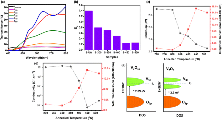
Fig. 3(a) shows the optical transmission spectra of Sas-grown, S300, S350, S400, S450, and S520. Apparently, the transmittance gradually increases with increasing the annealing temperature, and the maximum transmittance was observed in sample S400. The optical band gap was calculated for all the samples by using Tauc's equations.46 The calculated energy band gap of these samples decreases from ∼2.85 eV to 2.2 eV for the samples annealed at higher temperatures [Fig. 3(c)].
Usually, the amorphous semiconductors exhibit band-tailing due to the structural disorder which can be quantified as Urbach energy (Eu) shown in Fig. 3(b). The amorphous Sas-grown sample clearly having more defects shows highest Eu value which decreases by increasing annealing temperature, that indicate the defects are significantly reduced after annealing. The electrical conductivity (measured by four-probe) also decreases for the samples annealed at higher temperatures, as shown in Fig. 3(d). Fig. 3(c) and (d) also shows the optical transmission integrated over the wavelength from 400–800 nm plotted on right Y-axis, having clear correlation with the electronic properties. The results are explained by considering a band-model shown in Fig. 3(e). Although the band gap of V7O16 is higher than the V2O5, it still has high conductivity due to the presence of more V4+ content, that contribute extra electrons in 3d conduction band. Also, the amorphous and low-temperature annealed samples are expected to have large number of defects and oxygen vacancies, that can even push the Fermi level into the conduction band, making V7O16 a degenerate semiconductor.23 Therefore, the overall conductivity of mixed phase is higher than the V2O5 due to the presence of V7O16. On the other hand, the samples annealed at high-temperature are defects free, despite having a lower bandgap and the Fermi level lies in the band gap. The dynamic resistance versus temperature measurements also confirms the metallic behavior of mixed phase, where the resistance is found to increase with temperature compared to pure V2O5 showing a typical decrease in resistance with temperature of semiconducting behavior, as shown in ESI Fig. S1.† The correlation of transmission with conductivity in Fig. 3(c) and (d) can be explained by reflection and absorption caused by higher metallicity and defect states, respectively.
The photoluminescence (PL) and time-resolved-photoluminescence (TRPL) results of Sas-grown, S350, and S450 are shown in Fig. 4. The peaks in PL spectra were deconvoluted using Gaussian function. The highest intensity peaks at ∼438 nm, ∼507 nm, ∼530 nm can be assigned to the band-edge transitions from V3d conduction band to O2p valence band,37 matching the bandgap value of each sample measured by UV-vis measurement in Fig. 3. The peaks at longer wavelengths in NIR can be assigned to the electronic transitions in mid-gap states due to oxygen vacancies, and the peaks at shorter wavelengths in UV are due to the transitions from higher V3d states to O2p bands.37 Apparently, the more peaks in NIR are observed in amorphous and mixed phase samples due to large number of defects and oxygen vacancies compared to V2O5. The increased bandgap of mixed phase can be caused by the Burstein–Moss shift in PL spectra as a result of degenerate semiconducting behaviour of V7O16.23,47
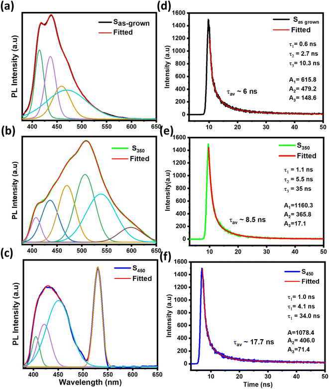 | ||
| Fig. 4 (a–c) The photoluminescence (PL) and (d–f) time-resolved photoluminescence (TRPL) spectra of Sas-grown, S350 and S450 samples. | ||
To further investigate the nature of defects, we have measured the carrier life using TRPL as shown in Fig. 4(b) of Sas-grown, S350, and S450. In TRPL, the peak intensity decay (ITRPL) with time (t) can be fitted using the following equation
The extracted fitting parameters and average decay time are shown in Table 2. The decay constants τ1 and τ2 attributes to the fast decay through trap-mediated recombination, while τ3 corresponds to slow decay through radiative recombination.37 The average decay time of S450 is higher compared than other two samples due to the reduction in oxygen vacancies in the samples, which agrees well with the previous observations.48 These results are in good agreement with the Urbach energy measurements shown in Fig. 3(b).
| Sample | A1 | A2 | A3 | τ1 (ns) | τ2 (ns) | τ3 (ns) | τaverage (ns) |
|---|---|---|---|---|---|---|---|
| Sas-grown | 615.8 | 479.2 | 148.6 | 0.6 | 2.7 | 10.3 | 6.1 |
| S350 | 1160.3 | 365.7 | 17.1 | 1.1 | 5.5 | 35.0 | 8.5 |
| S450 | 1078.4 | 406.0 | 71.4 | 1.0 | 4.1 | 33.9 | 17.7 |
Finally, we demonstrate the sensitivity of our mixed phase sample by heating and IR radiation as shown in Fig. 5(a) and (b) respectively. Fig. 5(a) illustrate the optical transmission taken before and after heating the sample at 200 °C outside and then transferred to the UV-vis spectroscopy. Interestingly, a clear change in the transmission was only observed for the wavelengths higher than ∼600 nm in near-IR (NIR) region. Indeed, no major change in the spectrum was observed in the visible range, indicating that these films are more sensitive to IR. Clearly, there will be some variations in temperature while taking the optical measurements, but the overall spectrum is always fully recovered as the samples is cooled back to the room temperature naturally.
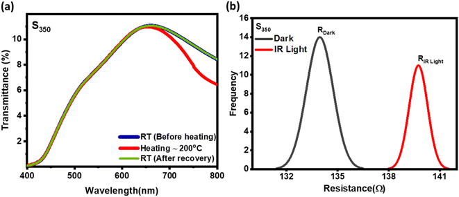 | ||
| Fig. 5 (a) UV-spectra of the mixed phase before and after heating at 200 °C (b) the distribution of resistance value before and after illumination of under IR radiation. | ||
Also, V7O16 being a degenerate semiconductor could also be suitable candidate for NIR plasmonics. Indeed, the broad peak ∼650 nm in the UV-vis spectrum could be due to the NIR plasmons absorption.23 Since the plasmonic frequency  is related to the carrier concentration (n) and the effective mass (m*), where e and ε0 are electronic charge and the permittivity of free space, respectively. The measured value of resonant frequency ∼4.6 × 10¹⁴ Hz gives the carrier concentration ∼1020 to 1021 cm−3, which is also consistent with our conductivity values considering the theoretical values of mobilities and effective mass of vanadium oxides (1–1.7me).49,50 The IR sensitivity in optical transmission is due to the plasmonic absorption and consistent with the earlier studied on the mixed phase of metallic VO2 and insulating V2O5.33 Also, the increase in resistance under IR radiation seen in Fig. 5(b) could be due to the electron–electron and electron–phonon scatterings as observed in metals and degenerate semiconductors in the resistance versus temperature measurements. Clearly, more low temperature transport measurements are required to further investigate the transport properties, but these results are encouraging for their promising use in smart-windows and IR sensors.
Conclusions
In conclusion, we provide a detailed in-depth understanding of electronic and optical properties of V7O16 and systematically tune the electronic and optical properties of a mixed phase by changing the V4+ and V5+ contents. We report a strong modulation in the conductivity and optical transmission with infrared radiation and temperature. These results are very promising for vanadium oxide based uncooled-IR sensors and smart windows that can be grown at low temperatures using a commercially viable cathodic vacuum arc-deposition technique.Conflicts of interest
There are no conflicts to declare.Acknowledgements
Anchal Rana acknowledges the research fellowship by BML Munjal University (BMU). Abhimanyu Rana would like to acknowledge SERB Core Research Grant CRG/2021/001l36 and HMCL-BMU Research Grant BMU/RESOICSR/HMCL/2022/001 for the financial support. The authors at BMU would like thank Mr Piyush Chaturvedi and Mr Naresh Verma for their help during the experiments.References
- A. Rogalski, Infrared Phys. Technol., 2002, 43, 187–210 CrossRef.
- J. Wang, H. Fang, X. Wang, X. Chen, W. Lu and W. Hu, Small, 2017, 13, 1–17 Search PubMed.
- A. Rogalski, J. Appl. Phys., 2003, 93, 4355–4391 CrossRef CAS.
- M. Strojnik, M. D'Acunto and A. Rogalski, Appl. Opt., 2016, 55, ITA1 CrossRef PubMed.
- D. Benyahia, Ł. Kubiszyn, K. Michalczewski, A. Kębłowski, P. Martyniuk, J. Piotrowski and A. Rogalski, Opt. Quantum Electron., 2016, 48, 1–7 CrossRef.
- K. Nakade, T. Kashiwagi, Y. Saiwai, H. Minami, T. Yamamoto, R. A. Klemm and K. Kadowaki, Sci. Rep., 2016, 6, 23178 CrossRef CAS.
- A. J. Kreisler and A. Gaugue, Supercond. Sci. Technol., 2000, 13, 1235 CrossRef CAS.
- F. J. Morin, Phys. Rev. Lett., 1959, 3, 34–36 CrossRef CAS.
- M. Imada, A. Fujimori and Y. Tokura, Rev. Mod. Phys., 1998, 70, 1039–1263 CrossRef CAS.
- C. Chen, X. Yi, J. Zhang and B. Xiong, Int. J. Infrared Millimeter Waves, 2001, 22, 53–58 CrossRef CAS.
- Q. Cheng, T. Bui, M. Almasri and S. Paradis, IEEE Sens. J., 2011, 11, 167–175 CAS.
- M. Nishikawa, T. Nakajima, T. Manabe, T. Okutani and T. Tsuchiya, Mater. Lett., 2010, 64, 1921–1924 CrossRef CAS.
- J. Jeong, N. Aetukuri, T. Graf, T. D. Schladt, M. G. Samant and S. S. P. Parkin, Science, 2013, 339, 1402–1405 CrossRef CAS PubMed.
- P. Shvets, O. Dikaya, K. Maksimova and A. Goikhman, J. Raman Spectrosc., 2019, 50, 1226–1244 CrossRef CAS.
- M. Yuan, T. Huang, S. Wang, R. Zhang, Y. Yang, W. Yang, W. Wei, T. Zhang, W. Dong, X. Chen and N. Dai, ACS Appl. Electron. Mater., 2019, 1, 2308–2313 CrossRef CAS.
- J. Huotari, J. Lappalainen, J. Eriksson, R. Bjorklund, E. Heinonen, I. Miinalainen, J. Puustinen and A. Lloyd Spetz, J. Alloys Compd., 2016, 675, 433–440 CrossRef CAS.
- M. Roppolo, C. B. Jacobs, S. Upreti, N. A. Chernova and M. S. Whittingham, J. Mater. Sci., 2008, 43, 4742–4748 CrossRef CAS.
- R. T. Rajendra Kumar, B. Karunagaran, D. Mangalaraj, S. K. Narayandass, P. Manoravi, M. Joseph and V. Gopal, Sens. Actuators, A, 2003, 107, 62–67 CrossRef CAS.
- M. M. Qazilbash, M. Brehm, B. G. Chae, P. C. Ho, G. O. Andreev, B. J. Kim, S. J. Yun, A. V. Balatsky, M. B. Maple, F. Keilmann, H. T. Kim and D. N. Basov, Science, 2007, 318, 1750–1753 CrossRef CAS PubMed.
- V. R. Morrison, R. P. Chatelain, K. L. Tiwari, A. Hendaoui, A. Bruhacs, M. Chaker and B. J. Siwick, Science, 2014, 346, 445–448 CrossRef CAS PubMed.
- P. T. P. Le, K. Hofhuis, A. Rana, M. Huijben, H. Hilgenkamp, G. A. J. H. M. Rijnders, J. E. ten Elshof, G. Koster, N. Gauquelin, G. Lumbeeck, C. Schüßler-Langeheine, H. Popescu, F. Fortuna, S. Smit, X. H. Verbeek, G. Araizi-Kanoutas, S. Mishra, I. Vaskivskyi, H. A. Dürr and M. S. Golden, Adv. Funct. Mater., 2020, 30, 1900028 CrossRef CAS.
- A. Rana, C. Li, G. Koster and H. Hilgenkamp, Sci. Rep., 2020, 10, 2–7 CrossRef PubMed.
- Q. Wang, M. Brier, S. Joshi, A. Puntambekar and V. Chakrapani, Phys. Rev. B, 2016, 94, 1–12 Search PubMed.
- S. Tepavcevic, H. Xiong, V. R. Stamenkovic, X. Zuo, M. Balasubramanian, V. B. Prakapenka, C. S. Johnson and T. Rajh, ACS Nano, 2012, 6, 530–538 CrossRef CAS PubMed.
- Y. Wang, K. Takahashi, K. Lee and G. Cao, Adv. Funct. Mater., 2006, 16, 1133–1144 CrossRef CAS.
- R. Baddour-Hadjean, M. Safrany Renard, N. Emery, L. T. N. Huynh, M. L. P. Le and J. P. Pereira-Ramos, Electrochim. Acta, 2018, 270, 129–137 CrossRef CAS.
- K. Schneider and W. Maziarz, Sensors, 2018, 2, 2–6 Search PubMed.
- M. Yu, X. Liu, Y. Wang, Y. Zheng, J. Zhang, M. Li, W. Lan and Q. Su, Appl. Surf. Sci., 2012, 258, 9554–9558 CrossRef CAS.
- J. Huotari, J. Lappalainen, J. Puustinen and A. Lloyd Spetz, Sens. Actuators, B, 2013, 187, 386–394 CrossRef CAS.
- T. K. Le, P. V. Pham, C. L. Dong, N. Bahlawane, D. Vernardou, I. Mjejri, A. Rougier and S. W. Kim, J. Mater. Chem. C, 2022, 10, 4019–4071 RSC.
- C. M. Lampert, Mater. Today, 2004, 7, 28–35 CrossRef CAS.
- S. Kumar, A. Qadir, F. Maury and N. Bahlawane, ACS Appl. Mater. Interfaces, 2017, 9, 21447–21456 CrossRef CAS PubMed.
- S. Y. Li, G. A. Niklasson and C. G. Granqvist, Thin Solid Films, 2012, 520, 3823–3828 CrossRef CAS.
- J. Huotari, R. Bjorklund, J. Lappalainen and A. L. Spetz, Procedia Eng., 2014, 87, 1035–1038 CrossRef CAS.
- C. K. Christensen, E. D. Bøjesen, D. R. Sørensen, J. H. Kristensen, J. K. Mathiesen, B. B. Iversen and D. B. Ravnsbæk, ACS Appl. Nano Mater., 2018, 1, 5071–5082 CrossRef CAS.
- Z. Yang, C. Ko and S. Ramanathan, Annu. Rev. Mater. Res., 2011, 41, 337–367 CrossRef CAS.
- T. K. Le, M. Kang, S. W. Han and S. W. Kim, RSC Adv., 2018, 8, 41317–41322 RSC.
- G. Silversmit, D. Depla, H. Poelman, G. B. Marin and R. De Gryse, J. Electron Spectrosc. Relat. Phenom., 2004, 135, 167–175 CrossRef CAS.
- A. Rana, A. Patra, M. Annamalai, A. Srivastava, S. Ghosh, K. Stoerzinger, Y.-L. Lee, S. Prakash, R. Y. Jueyuan, P. S. Goohpattader, N. Satyanarayana, K. Gopinadhan, M. M. Dykas, K. Poddar, S. Saha, T. Sarkar, B. Kumar, C. S. Bhatia, L. Giordano, Y. Shao-Horn and T. Venkatesan, Nanoscale, 2016, 8, 15597–15603 RSC.
- J. Mendialdua, R. Casanova and Y. Barbaux, J. Electron Spectrosc. Relat. Phenom., 1995, 71, 249–261 CrossRef CAS.
- G. Silversmit, D. Depla, H. Poelman, G. B. Marin and R. De Gryse, Surf. Sci., 2006, 600, 3512–3517 CrossRef CAS.
- R. Baddour-Hadjean, M. B. Smirnov, V. Y. Kazimirov, K. S. Smirnov and J. P. Pereira-Ramos, J. Raman Spectrosc., 2015, 46, 406–412 CrossRef CAS.
- A. G. S. Filho, O. P. Ferreira, E. J. G. Santos, J. M. Filho and O. L. Alves, Nano Lett., 2004, 4, 2099–2104 CrossRef.
- R. Baddour-Hadjean, M. B. Smirnov, K. S. Smirnov, V. Y. Kazimirov, J. M. Gallardo-Amores, U. Amador, M. E. Arroyo-de Dompablo and J. P. Pereira-Ramos, Inorg. Chem., 2012, 51, 3194–3201 CrossRef CAS PubMed.
- T. Blanquart, J. Niinistö, M. Gavagnin, V. Longo, M. Heikkilä, E. Puukilainen, V. R. Pallem, C. Dussarrat, M. Ritala and M. Leskelä, RSC Adv., 2013, 3, 1179–1185 RSC.
- M. Kang, S. W. Kim, Y. Hwang, Y. Um and J. W. Ryu, AIP Adv., 2013, 3, 052129 CrossRef.
- T. S. Moss, Proc. Phys. Soc. B, 1954, 67, 775 CrossRef.
- U. Özgür, A. Teke, C. Liu, S. J. Cho, H. Morkoç and H. O. Everitt, Appl. Phys. Lett., 2004, 84, 3223–3225 CrossRef.
- A. S. Barker, H. W. Verleur and H. J. Guggenheim, Phys. Rev. Lett., 1966, 17, 1286–1289 CrossRef CAS.
- M. M. Qazilbash, M. Brehm, B.-G. Chae, P.-C. Ho, G. O. Andreev, B.-J. Kim, S. J. Yun, A. V. Balatsky, M. B. Maple, F. Keilmann, H.-T. Kim and D. N. Basov, Science, 2007, 318, 1750–1753 CrossRef CAS PubMed.
Footnote |
| † Electronic supplementary information (ESI) available. See DOI: https://doi.org/10.1039/d3ra00752a |
| This journal is © The Royal Society of Chemistry 2023 |

