 Open Access Article
Surface modulation for highly efficient and stable perovskite solar cells†
Dongliang Bai‡
a,
Dexu Zheng‡c,
Shaoan Yang‡b,
Fengyang Yu*b,
Xuejie Zhua,
Lei Pengc,
Likun Wangb,
Jishuang Liuc,
Dong Yang*b and
Shengzhong (Frank) Liu *ab
*ab
aKey Laboratory of Applied Surface and Colloid Chemistry, Ministry of Education, Shaanxi Key Laboratory for Advanced Energy Devices, Shaanxi Engineering Lab for Advanced Energy Technology, School of Materials Science and Engineering, Shaanxi Normal University, Xi'an, 710119, China
bDalian National Laboratory for Clean Energy, Dalian Institute of Chemical Physics, Chinese Academy of Sciences, Dalian, 116023, China. E-mail: yufengyang@dicp.ac.cn; dongyang@dicp.ac.cn; szliu@dicp.ac.cn
cChina National Nuclear Power Co., Ltd., Beijing 100097, China
First published on 22nd September 2023
Abstract
Defects formed by halide ion escape and wettability of the perovskite absorber are essential limiting factors in achieving high performance of perovskite solar cells (PSCs). Herein, a series of ionic organic modulators are designed to contain halide anions to prevent defect formation and improve the surface tension of the perovskite absorber. It was found that the surface modulator containing Br anions is the most effective one due to its capability in bonding with the undercoordinated Pb2+ ions to reduce charge recombination. Moreover, this surface modulator effectively creates a suitable energy level between the perovskite and hole transport layer to promote carrier transfer. In addition, the surface modulator forms a chemisorbed capping layer on the perovskite surface to improve its hydrophobicity. As a result, the efficiency of PSCs based on surface modulators containing Br anion enhances to 23.32% from 21.08% of the control device. The efficiency of unencapsulated PSCs with a surface modulator retains 75.42% of its initial value under about 35% humidity stored in the air for 28 days, while the control device only maintained 44.49% of its initial efficiency. The excellent stability originates from the hydrophobic perovskite surface after capping the surface modulator.
Introduction
In recent years, perovskite solar cells (PSCs) have attracted much attention in the photovoltaic research community due to their remarkable optoelectronic properties such as long carrier diffusion lengths, direct tunable bandgap, high absorption coefficients, and extremely low exciton binding energy.1–3 The power conversion efficiency (PCE) of PSCs has rapidly enhanced to 25.7% since their first demonstration in 2009.4,5 The photoelectric properties of the charge transport layer and perovskite absorber are the key influencing factors in the high performance of PSCs according to previous reports.6,7 There are numerous studies focused on charge transport layer such as novel materials, modification, and passivation to successfully improve the efficiency and stability of perovskite devices.8–13 For the perovskite absorber, its properties including surface roughness, crystallinity, grain size, and defects limit the performance of PSCs.14–18 Among these restraining factors, the bulk and interface defects of perovskite absorbers particularly impact the charge transfer dynamic of perovskite devices.Defects are divided into shallow-level defects and deep-level defects. The charges captured by the shallow-level defects will return to the conduction band/valence band and then be collected by the electrode. Therefore, these shallow-level defects have little influence on carrier recombination. However, the charges trapped by the deep-level defects will inevitably suffer non-radiative recombination, and it has a great effect on charge transfer in PSCs.19,20 In general, deep-level defects are mainly located at grain boundaries and the interface with a high formation energy,21,22 and the density of deep defects at the perovskite surface is around two orders of magnitude higher than that of the bulk.23 The surface defects thus dominate the carrier recombination in PSCs. Therefore, effective surface modification to reduce the defects is essential for improving the performance of PSCs.24,25 To date, post-treatment by coating passivation agents, including Lewis acid-base, alkyl ammonium halide, and organic molecules on the perovskite surface are considered efficient methods to decrease the surface defects. Shi et al.26 added 6,6′-dithiodinicotinic acid and urea as the additives, and the PCE improved from 16.76 to 20.64%. Wang et al.27 introduced thiourea (Lewis acid-base) into the CH3NH3PbI3 precursor, the photoelectric performance of the perovskite layer improved, and optimized efficiency was up to 19.80%. Ye et al.28 compared the passivation capacity of three structurally similar alkyl ammonium salts and found that the water contact angle gradually increased when increasing the number of carbon atoms in the alkane. The PCE was enhanced to 21.22% with a great improvement in humidity stability. Hu et al.29 employed organic molecule 4-(aminomethyl) benzoic acid hydroiodide as an organic cation in the CH3NH3PbI3 precursor solution. The device showed good stability, and the PCE increased to 15.6%. https://pubs.acs.org/action/doSearch?field1=Contrib%26text1=Yevgeny++Rakita et al.30 used alcoholic solutions of alkyl ammonium or halides monovalent alkali metal to treat metal (Pb or Sn) films. In this way, halide perovskite films had been formed without the use of toxic Pb2+ solutions. Cheng et al.31 employed pyridine-terminated conjugated small organic molecules to link the NiOx and perovskite layers, and the efficiency improved from 12.53% to 17.00%.
In addition, the capping layer above the perovskite absorber effectively inhibits ion migration and diffusion at the surface and efficiently protects the perovskite degradation from the influence of water and oxygen in the atmosphere. Zhong et al.32 added a polymer mixture of polyvinylpyrrolidone (PVP) and polyethylene glycol into the PbI2 precursor solution, and there was an efficiency enhancement of 30% over the pristine one. Polymer mixture-modified PSC also represents better air stability. Sandoval-Torrientes et al.33 used a variety of chemically modified fullerenes to prepare perovskite/fullerene blends, and the PCE of ETL-free perovskite devices improved to 14.3%. Chen et al.34 prepare 2D PEA2PbI4 capping layers on top of a 3D perovskite film, and a high efficiency of 18.51% with drastically improved stability was obtained.
In this study, we developed an ionic organic modulator, 1-hexadecyl-3-methylimidazolium hexafluorophosphate (1-h-3-MIHFP), 1-hexadecyl-3-methylimidazolium chloride (1-h-3-MICl) and 1-hexadecyl-3-methylimidazolium bromide (1-h-3-MIBr) as the surface modulator layers and compared their effect on the performance of PSCs. Experimental results revealed that all these surface modulator layers effectively enhanced the carrier lifetime and reduced the surface defects of the perovskite absorber. The perovskite devices with 1-h-3-MIBr exhibited the best performance. The efficiency of PSCs based on 1-h-3-MIBr increased to 23.32% from 21.08% of the control device. Meanwhile, the long-term environmental stability of the device based on 1-h-3-MIBr is better than that of the control perovskite device. The efficiency of the unencapsulated perovskite device with 1-h-3-MIBr was maintained at 75.42% of its initial value under about 35% humidity stored in the air for 28 days, while the control device only retained 44.49% of its initial efficiency. The excellent stability contributed to the hydrophobic surface after modifying 1-h-3-MIBr, which effectively prohibited moisture permeation. Halogen atoms have a great influence on passivation and hydrophobicity ability. Therefore, it is meaningful to choose a passivant containing suitable halogen, which would provide an insightful strategy for high-efficiency and stable perovskite devices.
Experiments
Materials
Dimethylformamide (DMF), dimethyl sulfoxide (DMSO), chlorobenzene (CB), isopropanol (IPA), 4-tert-butylpyridine (t-BP), acetonitrile, 2-propanol and bis(trifluoromethylsulfonyl) imidelithium salt (Li-TFSI) were purchased from Sigma-Aldrich. Tin (IV) oxide colloidal dispersion was purchased from Alfa Aesar. 1-h-3-MIHFP, 1-h-3-MICl, 1-h-3-MIBr were purchased from TCI. Methylammonium iodide (MAI), methylammonium chloride (MACl), Spiro-OMeTAD, FK209 Co(III) TFSI salt, lead(II) iodide (PbI2, 99.99%) and formamidinium iodide (H2N = CHNH2I; FAI) were purchased from Xi'an Polymer Light Technology Corp. All materials were used as received without any further purification.Device fabrication
The glass/FTO substrates were ultrasonically cleaned using deionized water, acetone, and IPA for 30 min, sequentially. The cleaned substrates were treated with O2 plasma for 5 min, and then the SnO2 colloidal solution (the volume ratio of SnO2 colloidal precursor and water was 1![[thin space (1/6-em)]](https://www.rsc.org/images/entities/char_2009.gif) :
:![[thin space (1/6-em)]](https://www.rsc.org/images/entities/char_2009.gif) 5) was spin-coated on the glass/FTO substrate at 3000 rpm for 30 s. The glass/FTO/SnO2 samples were annealed at 150 °C for 30 min in the air. 1.5 mmol PbI2 was dissolved in 1 mL mixed solution (DMF
5) was spin-coated on the glass/FTO substrate at 3000 rpm for 30 s. The glass/FTO/SnO2 samples were annealed at 150 °C for 30 min in the air. 1.5 mmol PbI2 was dissolved in 1 mL mixed solution (DMF![[thin space (1/6-em)]](https://www.rsc.org/images/entities/char_2009.gif) :
:![[thin space (1/6-em)]](https://www.rsc.org/images/entities/char_2009.gif) DMSO = 9
DMSO = 9![[thin space (1/6-em)]](https://www.rsc.org/images/entities/char_2009.gif) :
:![[thin space (1/6-em)]](https://www.rsc.org/images/entities/char_2009.gif) 1). 70 mg FAI, 3 mg MAI, and 7 mg MACl were dissolved in IPA. 50 μL PbI2 solution was deposited by spin-coating at 2000 rpm for 30 s and then annealed at 80 °C for 1 min. 200 μL mixed IPA solution was deposited by spin-coating at 2000 rpm for 30 s. The thin films were annealed at 150 °C for 15 min in the air. After cooling to room temperature, surface modulator layers were deposited by spin-coating at 4000 rpm for 30 s using 2 mg mL−1 organic salts dissolved IPA. HTL solution was deposited by spin-coating at 3500 rpm for 30 s without further annealing. To obtain the HTL solution, 72.3 mg spiro-OMeTAD powder was dissolved in 1 mL CB with additives of 35 μL LiTFSI solution (260 mg mL−1 in acetonitrile) and 28.8 μL t-BP. Finally, 80 nm-thick Au was deposited using thermal evaporation.
1). 70 mg FAI, 3 mg MAI, and 7 mg MACl were dissolved in IPA. 50 μL PbI2 solution was deposited by spin-coating at 2000 rpm for 30 s and then annealed at 80 °C for 1 min. 200 μL mixed IPA solution was deposited by spin-coating at 2000 rpm for 30 s. The thin films were annealed at 150 °C for 15 min in the air. After cooling to room temperature, surface modulator layers were deposited by spin-coating at 4000 rpm for 30 s using 2 mg mL−1 organic salts dissolved IPA. HTL solution was deposited by spin-coating at 3500 rpm for 30 s without further annealing. To obtain the HTL solution, 72.3 mg spiro-OMeTAD powder was dissolved in 1 mL CB with additives of 35 μL LiTFSI solution (260 mg mL−1 in acetonitrile) and 28.8 μL t-BP. Finally, 80 nm-thick Au was deposited using thermal evaporation.
Characterization
The J–V curves were measured using a xenon-lamp-based solar simulator (Newport, Class AAA Solar Simulator) with a source meter (Keithley B2902A Source Meter) under AM 1.5G illumination. The illumination was calibrated using an NREL-traceable KG5-filtered silicon reference cell. The scan speed was 0.1 V s−1, and the scan delay time was 10 ms. All devices were attached with a metal mask with a circle-type aperture of 0.1 cm2 to avoid light scattering from the metal electrode into the device during the measurement. The EQE was measured using a Crowntech QTest Station 2000ADI system. Steady-state PL (excitation at 532 nm) measurements were carried out on an Edinburgh Instruments Ltd (FLS980) instrument. TRPL spectra were collected using an Edinburgh Instruments (FLS980) fluorescence spectrometer with the time-correlated single-photon counting method. SEM images were recorded using a field emission scanning electron microscope (SU8020). The adsorption spectra were recorded using a PerkinElmer 10 UV-Lambda 950 instrument. The static water contact angles were measured using a contact angle meter (DSA100). XPS data were measured on a Thermo Fisher Scientific (K-Alpha system) instrument using Al Kα as the exciting X-ray source at a pressure of 1 × 10⁻⁸ Pa.Results and discussion
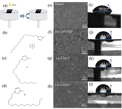
The different surface modulator layers were fabricated by the spin-coating method, as shown in Fig. 1a. Fig. 1b–d give the molecular structures of various surface modulators. It is clear that the difference between surface modulators is the halide anions. The morphologies of perovskite films without and with surface modulator layers were studied by scanning electron microscopy (SEM). Fig. 1e–h shows the top-view SEM images of the pristine perovskite and modified perovskite films. It can be seen that the morphology does not change obviously when covered by chemisorbed capping layers.Fig. 1i–l shows the water contact angles of the perovskite film without and with surface modulator layers. The same concentration (2 mg mL−1) of the passivant was spun onto the perovskite film. The static water contact angles of control and optimized perovskite films were measured. The contact angle of the pristine perovskite film was 57.22°, and it dramatically increased to 81.55°, 83.67°, and 91.25° for the 1-h-3-MIHFP, 1-h-3-MICl, and 1-h-3-MIBr, respectively. The significantly increased contact angles are due to the hydrophobic organic moieties in surface modulators. The perovskite covered by 1-h-3-MIBr showed the largest water contact angle compared to other surface modulators, likely due to the stronger molecules symmetry caused by a larger ionic radius of Br. The large water contact angle would enhance the barrier for moisture permeation to improve the stability of perovskite.35
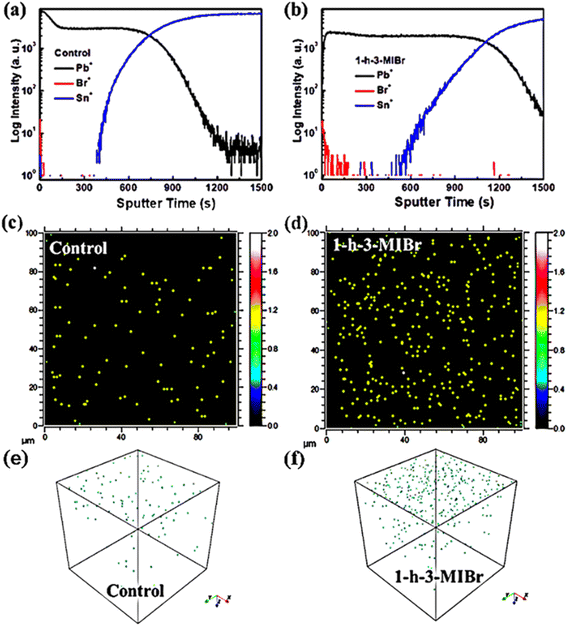
The perovskite film with 1-h-3-MIBr was selected as the representation, and positive secondary ion depth profiles were measured to investigate the distribution of the elements using a surface modulator. Fig. 2a and b show the time-of-flight secondary-ion mass spectrometry (TOF-SIMS) results of the perovskite without and with 1-h-3-MIBr deposited on FTO substrates. Fig. S1† shows the photos of the samples before and after sputter etching. Approximately, the positions of various ions can be detected by the depth profiles during the sputtering process. The traces for ions directly related to FA0.95MA0.05PbI3 (Pb+), FTO (Sn+), and 1-h-3-MIBr (Br+) when sputtering depth of the films. The trace of the Pb+ position appears in the plateau part and then decreases with increasing sputtering time. The Pb+ and Sn+ positions are simultaneously observed, which suggests the ion migration into FTO from perovskite. It cannot detect the Br+ position in pristine perovskite (Fig. 2a), and this position clearly identifies in perovskite with 1-h-3-MIBr (Fig. 2b). The signal of the Br+ position quickly disappears with increasing sputtering time, indicating that1-h-3-MIBr forms an ultrathin film on perovskite. Fig. 2c, d, and f, g show the two-dimensional and three-dimensional depth profiles of Br elements for perovskite without and with 1-h-3-MIBr, respectively. For the pristine sample, negligible Br+ was detected likely due to the cross-contamination during the fabrication/measurement process. For a sample of perovskite with 1 h-3MIBr, the Br elements are mostly focused on the perovskite surface. TOF-SIMS results revealed that the surface modulator forms a uniform thin film on the perovskite surface.
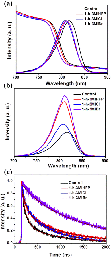
The optical and charge transfer of the perovskite covered by different surface modulator layers were measured. Fig. 3a shows the normalized absorption and photoluminescence (PL) spectra of perovskite without and with different surface modulator layers. It is clear that the absorb edges and PL peaks of the perovskite show a blue shift, which should be caused by the reduced defects by surface modulator layers,36 as discussed below. Fig. 3b shows the steady-state PL spectra of the perovskite with and without surface modulators. All surface modulators could improve the peak intensity, and the perovskite with 1-h-3-MIBr gives the strongest PL intensity, demonstrating the fewest charge recombination.
The time-resolved PL (TRPL) measurements were tested to investigate the carrier transfer dynamics. Fig. 3c shows the TRPL spectra of the perovskite without and with surface modulator layers. The carrier decay lifetime (τ) can be fitted by an exponential equation.37,38 As a result, the carrier decay lifetimes are 328.33 ns, 646.71 ns, 498.88 ns, and 1265.60 ns for pristine perovskite, perovskite with 1-h-3-MIHFP, 1-h-3-MICl, and 1-h-3-MIBr, respectively. The perovskite with 1-h-3-MIBr showed the longest carrier lifetime, indicating efficient charge carrier dissociation and suppressed non-radiative recombination.
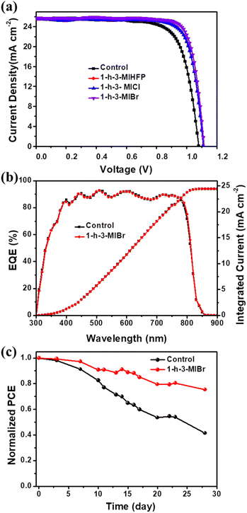
The perovskite devices were fabricated to evaluate the influence of different surface modulators. The cross-sectional SEM image of the completed device is shown in Fig. S2.† FTO and Au have been used as the anode and cathode, respectively. SnO2 and 2,2′,7,7′-tetrakis(N,N-di-p-methoxyphenylamine)-9,9′-spirobifluorene (spiro-OMeTAD) were employed as the electron transport layer (ETL) and hole transport layer (HTL), respectively. FA0.95MA0.05PbI3 was adopted as an absorber, and different ionic organic modulators are developed as surface modulator layers. Fig. 4a shows the current density–voltage (J–V) curves of PSCs without and with various surface modulator layers, and the key photovoltaic parameters including short-circuit current density (Jsc), open-circuit voltage (Voc), fill factor (FF) and PCE are summarized in Table 1. The PCE of the best control perovskite device was 21.08% with Jsc of 25.67 mA cm−2, Voc of 1.08 V, and FF of 75.87%. When the perovskite is covered by surface modulators, both Voc and FF are enhanced. The perovskite device with 1-h-3-MIBr exhibits the largest Voc of 1.12 V and FF of 80.95%, yielding the highest efficiency of 23.32%. The high Voc and FF are attributed to the long carrier lifetime (Fig. 3b and c) and the decreased carrier recombination (as discussed below) when using 1-h-3-MIBr surface modulator. In addition, the performance of our device with passivant has been compared with data from previous reports (Table S1†), and it is clear that our device shows high efficiency. Fig. 4b shows the external quantum efficiency (EQE) measurements of the perovskite devices without and with 1-h-3-MIBr. The integrated photocurrents are 24.41 mA cm−2 and 24.42 mA cm−2, in agreement with J–V results.
| Device | Voc (V) | Jsc (mA cm−2) | FF (%) | PCE (%) |
|---|---|---|---|---|
| Control | 1.08 | 25.68 | 75.87 | 21.08 |
| 1-h-3-MIHFP | 1.11 | 25.89 | 79.34 | 22.81 |
| 1-h-3-MICl | 1.09 | 25.79 | 79.95 | 22.50 |
| 1-h-3-MIBr | 1.12 | 25.84 | 80.95 | 23.32 |
In addition, 13 individual devices for each surface modulator layer have been fabricated and tested to accurately quantify the repeatability of the perovskite devices. The parameter distribution histograms are shown in Fig. S3,† and the statistics are listed in Tables S2–S5.† All the devices exhibit good repeatability with a small standard deviation, indicating that these ionic organic modulators are excellent surface modulators in the PSCs. The above results revealed that 1-h-3-MIBr is the most effective surface modulator, and the below discussions thereby focus on perovskite with 1-h-3-MIBr.
Environmental stability is a key characteristic of PSCs. Fig. 4c shows the long-term environmental stability of the perovskite devices without and with 1-h-3-MIBr. The PCE of the unencapsulated device with 1-h-3-MIBr maintains 75.42% of its initial efficiency under about 35% humidity stored in the air for 28 days. However, the efficiency of the control device without 1-h-3-MIBr only holds 44.49% of its initial value. The excellent environmental stability originates from the hydrophobic perovskite surface covered by 1-h-3-MIBr (Fig. 1l), which successfully blocks the moisture permeation into the device.
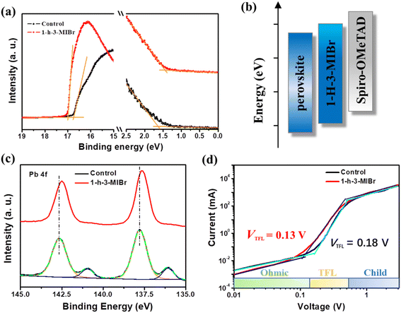
Fig. 5a shows the ultraviolet photoelectron spectrometer (UPS) results of the perovskite without and with 1-h-3-MIBr. The Fermi level (EF) is calculated by equation EF = Ecut − 21.22 eV, where Ecut is the cut-off binding energy, and 21.22 eV is the emission energy of the helium irradiation. The Ecut of pristine perovskite and perovskite with 1-h-3-MIBr are 16.76 eV and 17.01 eV, respectively. Thus, the EF of the pristine perovskite and perovskite with 1-h-3-MIBr are −4.46 eV and −4.21 eV, respectively. The Fermi edge (Eedge) of the pristine perovskite and perovskite with 1-h-3-MIBr are 1.62 eV and 1.44 eV (Fig. 5a), respectively. Therefore, the valence band (EVB) of the pristine perovskite and the perovskite with 1-h-3-MIBr are −6.08 eV and −5.65 eV according to the equation of EVB = EF − Eedge. The energy–level diagram is described in Fig. 5b. The EVB of perovskite based on 1-h-3-MIBr is closer to spiro-OMeTAD (HTL) than that of pristine perovskite, leading to larger Voc due to less energy loss during charge transfer.39
X-ray photoelectron spectra (XPS) were collected to identify the interaction between the perovskite and 1-h-3-MIBr. Fig. 5c shows the XPS results of Pb 4f for the pristine perovskite and perovskite with 1-h-3-MIBr. The binding energy scale for XPS was calibrated according to the C 1 s line at 284.8![[thin space (1/6-em)]](https://www.rsc.org/images/entities/char_2009.gif) eV. There is a small binding energy at 141.0 eV, corresponding to the Pb 0 core level for the pristine perovskite. This binding energy disappears after covering 1-h-3-MIBr thin film. Meanwhile, the Pb 4f peaks of the perovskite with 1-h-3-MIBr shift to a lower binding energy compared to the pristine perovskite. These results indicate that the 1-h-3-MIBr reacts with uncoordinated Pb2+ ions, which would reduce the defects due to the decreased ion vacancy.
eV. There is a small binding energy at 141.0 eV, corresponding to the Pb 0 core level for the pristine perovskite. This binding energy disappears after covering 1-h-3-MIBr thin film. Meanwhile, the Pb 4f peaks of the perovskite with 1-h-3-MIBr shift to a lower binding energy compared to the pristine perovskite. These results indicate that the 1-h-3-MIBr reacts with uncoordinated Pb2+ ions, which would reduce the defects due to the decreased ion vacancy.
Fig. 5d shows the dark current–voltage (I–V) curves of the single carrier devices. The defect density (Nt) can be calculated by the equation of Nt = 2ε0εrVTFL/eL2.40 Where the ε0 is the vacuum permittivity, εr is the relative dielectric constant of perovskite, e is the element charge, and L is the thickness of the perovskite film. The VTFL is the trap-filled limit voltage, which can be obtained from the dark I–V curves. The VTFL values are 0.13 V and 0.18 V for the pristine perovskite and perovskite with 1-h-3-MIBr, respectively. Therefore, the defect densities are 3.62 × 10¹⁴ and 2.58 × 1014 cm3 for the control perovskite and perovskite with 1-h-3-MIBr, respectively. The defect density calculation results are in good agreement with the above analysis. The low defect density significantly decreases the charge recombination, resulting in high Voc and FF.
Conclusion
In summary, we developed several ionic organic modulators including 1-h-3-MIHFP 1-h-3-MICl, and 1-h-3-MIBr as the surface modulator layers to modify the surface properties of the perovskite film. The perovskite device based on 1-h-3-MIBr exhibited the highest efficiency of 23.32% with improved Voc and FF. The high performance is caused by the suitable energy level, enhanced carrier lifetime, and reduced defects, which lead to effective carrier transfer and decreased charge recombination. The 1-h-3-MIBr forms the uniform thin film on the perovskite to increase the surface hydrophobicity, which inhibits the moisture permeation, leading to the meaningfully improved long-term environmental stability of PSCs. This research provides an insightful strategy for the selection of post-treatment materials for high-efficiency and stable perovskite devices.Conflicts of interest
There are no conflicts to declare.Acknowledgements
The authors acknowledge support from the National Natural Science Foundation of China (Grant No. 61975106), the Strategic Priority Research Program of the Chinese Academy of Sciences (Grant No. XDA17040506), the National University Research Fund (Grant No. GK261001009), the Innovative Research Team (Grant No. IRT_14R33), the 111 Project (Grant No. B14041), and the Shaanxi Science and Technology Department (20201101012).References
- Q.-Q. Chu, B. Cheng and B. Fang, Matter, 2022, 5, 2584–2586 CrossRef CAS.
- Q.-Q. Chu, B. Ding, Q. Qiu, Y. Liu, C.-X. Li, C.-J. Li, G.-J. Yang and B. Fang, J. Mater. Chem. A, 2018, 6, 8271–8279 RSC.
- X. Zheng, Y. Hou, C. Bao, J. Yin, F. Yuan, Z. Huang, K. Song, J. Liu, J. Troughton, N. Gasparini, C. Zhou, Y. Lin, D.-J. Xue, B. Chen, A. K. Johnston, N. Wei, M. N. Hedhili, M. Wei, A. Y. Alsalloum, P. Maity, B. Turedi, C. Yang, D. Baran, T. D. Anthopoulos, Y. Han, Z.-H. Lu, O. F. Mohammed, F. Gao, E. H. Sargent and O. M. Bakr, Nat. Energy, 2020, 5, 131–140 CrossRef CAS.
- NREL, http://www.nrel.gov/pv/cell-efficiency.html.
- A. Kojima, K. Teshima, Y. Shirai and T. Miyasaka, J. Am. Chem. Soc., 2009, 131, 6050–6051 CrossRef CAS PubMed.
- D. Yang, R. Yang, K. Wang, C. Wu, X. Zhu, J. Feng, X. Ren, G. Fang, S. Priya and S. Liu, Nat. Commun., 2018, 9, 3239 CrossRef PubMed.
- J. Feng, X. Zhu, Z. Yang, X. Zhang, J. Niu, Z. Wang, S. Zuo, S. Priya, S. Liu and D. Yang, Adv. Mater., 2018, 30, 1801418 CrossRef PubMed.
- K. Wang, X. Liu, R. Huang, C. Wu, D. Yang, X. Hu, X. Jiang, J. C. Duchamp, H. Dorn and S. Priya, ACS Energy Lett., 2019, 4, 1852–1861 CrossRef CAS.
- Z.-W. Gao, Y. Wang and W. C. H. Choy, Adv. Energy Mater., 2022, 12, 2104030 CrossRef CAS.
- Q.-Q. Chu, B. Cheng and B. Fang, Matter, 2022, 5, 2444–2446 CrossRef CAS.
- M. Du, S. Zhao, L. Duan, Y. Cao, H. Wang, Y. Sun, L. Wang, X. Zhu, J. Feng, L. Liu, X. Jiang, Q. Dong, Y. Shi, K. Wang and S. Liu, Joule, 2022, 6, 1931–1943 CrossRef CAS.
- X. Ren, D. Yang, Z. Yang, J. Feng, X. Zhu, J. Niu, Y. Liu, W. Zhao and S. F. Liu, ACS Appl. Mater. Interfaces, 2017, 9, 2421–2429 CrossRef CAS PubMed.
- Y. Chen, X. Zuo, Y. He, F. Qian, S. Zuo, Y. Zhang, L. Liang, Z. Chen, K. Zhao, Z. Liu, J. Gou and S. Liu, Advanced Science, 2021, 8, 2001466 CrossRef CAS PubMed.
- D. Yang, R. Yang, X. Ren, X. Zhu, Z. Yang, C. Li and S. Liu, Adv. Mater., 2016, 28, 5206–5213 CrossRef CAS PubMed.
- Z. Wu, E. Bi, C. Li, L. Chen, Z. Song and Y. Yan, Sol. RRL, 2023, 7, 2200571 CrossRef CAS.
- S.-Y. Hsiao, H.-L. Lin, W.-H. Lee, W.-L. Tsai, K.-M. Chiang, W.-Y. Liao, C.-Z. Ren-Wu, C.-Y. Chen and H.-W. Lin, Adv. Mater., 2016, 28, 7013–7019 CrossRef CAS PubMed.
- H. Shen, Y. Wu, J. Peng, T. Duong, X. Fu, C. Barugkin, T. P. White, K. Weber and K. R. Catchpole, ACS Appl. Mater. Interfaces, 2017, 9, 5974–5981 CrossRef CAS PubMed.
- F. Wang, P. Wai-Keung Fong, Z. Ren, H.-L. Xia, K. Zhou, K. Wang, J. Zhu, X. Huang, X.-Y. Liu, H. Wang, Y. Shi, H. Lin, Q. Zhu, G. Li and H. Hu, J. Energy Chem., 2022, 73, 599–606 CrossRef CAS.
- L. Fu, H. Li, L. Wang, R. Yin, B. Li and L. Yin, Energy Environ. Sci., 2020, 13, 4017–4056 RSC.
- Y. Shao, Y. Fang, T. Li, Q. Wang, Q. Dong, Y. Deng, Y. Yuan, H. Wei, M. Wang, A. Gruverman, J. Shield and J. Huang, Energy Environ. Sci., 2016, 9, 1752–1759 RSC.
- J. Chen and N.-G. Park, Adv. Mater., 2019, 31, 1803019 CrossRef CAS PubMed.
- Y. Yuan, T. Li, Q. Wang, J. Xing, A. Gruverman and J. Huang, Sci. Adv., 2017, 3, e1602164 CrossRef PubMed.
- Z. Ni, C. Bao, Y. Liu, Q. Jiang, W.-Q. Wu, S. Chen, X. Dai, B. Chen, B. Hartweg, Z. Yu, Z. Holman and J. Huang, Science, 2020, 367, 1352–1358 CrossRef CAS PubMed.
- J. Xia, C. Liang, H. Gu, S. Mei, S. Li, N. Zhang, S. Chen, Y. Cai and G. Xing, Energy Environ. Mater., 2023, 6, e12296 CrossRef CAS.
- G. Wu, R. Liang, M. Ge, G. Sun, Y. Zhang and G. Xing, Adv. Mater., 2022, 34, 2105635 CrossRef CAS PubMed.
- Z.-E. Shi, J.-Y. Long, C.-W. Li, S.-Y. Hsieh, Y.-S. Hsiao, C.-P. Chen and Y.-H. Yu, Sustainable Energy Fuels, 2022, 6, 1950–1958 RSC.
- S. Wang, Z. Ma, B. Liu, W. Wu, Y. Zhu, R. Ma and C. Wang, Sol. RRL, 2018, 2, 1800034 CrossRef.
- X. Ye, H. Cai, Q. Sun, T. Xu, J. Ni, J. Li and J. Zhang, Org. Electron., 2022, 106, 106542 CrossRef CAS.
- Y. Hu, Z. Zhang, A. Mei, Y. Jiang, X. Hou, Q. Wang, K. Du, Y. Rong, Y. Zhou, G. Xu and H. Han, Adv. Mater., 2018, 30, 1705786 CrossRef PubMed.
- Y. Rakita, S. Gupta, D. Cahen and G. Hodes, Chem. Mater., 2017, 29, 8620–8629 CrossRef CAS.
- H. Cheng, Y. Li, G. Zhao, K. Zhao and Z.-S. Wang, ACS Appl. Mater. Interfaces, 2019, 11, 28960–28967 CrossRef CAS PubMed.
- M. Zhong, L. Chai, Y. Wang and J. Di, J. Alloys Compd., 2021, 864, 158793 CrossRef CAS.
- R. Sandoval-Torrientes, J. Pascual, I. García-Benito, S. Collavini, I. Kosta, R. Tena-Zaera, N. Martín and J. L. Delgado, ChenSusChem, 2017, 10, 2023–2029 CrossRef CAS PubMed.
- P. Chen, Y. Bai, S. Wang, M. Lyu, J.-H. Yun and L. Wang, Adv. Funct. Mater., 2018, 28, 1706923 CrossRef.
- A. H. Proppe, M. Wei, B. Chen, R. Quintero-Bermudez, S. O. Kelley and E. H. Sargent, J. Am. Chem. Soc., 2019, 141, 14180–14189 CrossRef CAS PubMed.
- Q. Cai, Z. Lin, W. Zhang, X. Xu, H. Dong, S. Yuan, C. Liang and C. Mu, J. Phys. Chem. Lett., 2022, 13, 4598–4604 CrossRef CAS PubMed.
- E. V. Péan, S. Dimitrov, C. S. De Castro and M. L. Davies, Phys. Chem. Chem. Phys., 2020, 22, 28345–28358 RSC.
- J. Feng, Z. Yang, D. Yang, X. Ren, X. Zhu, Z. Jin, W. Zi, Q. Wei and S. Liu, Nano Energy, 2017, 36, 1–8 CrossRef CAS.
- M. Rai, L. H. Wong and L. Etgar, J. Phys. Chem. Lett., 2020, 11, 8189–8194 CrossRef CAS PubMed.
- N. Zhou, Y. Shen, Y. Zhang, Z. Xu, G. Zheng, L. Li, Q. Chen and H. Zhou, Small, 2017, 13, 1700484 CrossRef PubMed.
Footnotes |
| † Electronic supplementary information (ESI) available. See DOI: https://doi.org/10.1039/d3ra00809f |
| ‡ These three authors contributed equally to this study and share the first authorship. |
| This journal is © The Royal Society of Chemistry 2023 |

