 Open Access Article
First-principles study of SiC and GeC monolayers with adsorbed non-metal atoms†
Chu Viet Haa,
L. T. Hab,
Do Thi Huea,
Duy Khanh Nguyenc,
Dang Tuan Anha,
J. Guerrero-Sanchezd and
D. M. Hoat *ef
*ef
aFaculty of Physics, TNU-University of Education, Thai Nguyen, 250000, Vietnam
bInstitute of Science and Technology, TNU-University of Science, Thai Nguyen, 250000, Vietnam
cHigh-Performance Computing Lab (HPC Lab), Information Technology Center, Thu Dau Mot University, Binh Duong Province, Vietnam
dUniversidad Nacional Autónoma de México, Centro de Nanociencias y Nanotecnología, Apartado Postal 14, Ensenada, Baja California Código Postal 22800, Mexico
eInstitute of Theoretical and Applied Research, Duy Tan University, Ha Noi 100000, Vietnam. E-mail: dominhhoat@duytan.edu.vn
fFaculty of Natural Sciences, Duy Tan University, Da Nang 550000, Vietnam
First published on 16th May 2023
Abstract
Chemical adsorption of non-metal atoms may lead to the emergence of novel features in two-dimensional (2D) materials. In this work, the electronic and magnetic properties of graphene-like XC (X = Si and Ge) monolayers with adsorbed H, O, and F atoms are investigated using spin-polarized first-principles calculations. Deeply negative adsorption energies suggest strong chemical adsorption on XC monolayers. Despite the non-magnetic nature of both host monolayer and adatom, SiC is significantly magnetized by H adsorption inducing the magnetic semiconductor nature. Similar features are observed in GeC monolayers upon adsorbing H and F atoms. In all cases, an integer total magnetic moment of 1 μB is obtained, originating mainly from adatoms and their neighbor X and C atoms. In contrast, O adsorption preserves the non-magnetic nature of SiC and GeC monolayers. However, the electronic band gaps exhibit significant reduction of the order of 26% and 18.84%, respectively. These reductions are consequences of the middle-gap energy branch generated by the unoccupied O-pz state. The results introduce an efficient approach to develop d0 2D magnetic materials to be applied in spintronic devices, as well as to widen the working region of XC monolayers in optoelectronic applications.
I. Introduction
Since its first successful exfoliation by Novoselov et al.1 in 2004, graphene (a two-dimensional (2D) counterpart of carbon) has attracted enormous interest of researchers for both fundamental study and technological applications due to its intriguing mechanical, chemical, and physical properties.2–4 Such that graphene has been explored as an excellent candidate for a wide range of applications as photonics and optoelectronics,5,6 catalysis,7,8 gas sensing8,9 and spintronics,10,11 among others. The interest has been extended also to other graphene analogues based on the IVA group such as silicene (2D counterpart of silicon)12,13 and germanene (2D counterpart of germanium).14,15 However, graphene, silicene, and germanene monolayers have been found to be semimetals with valence band and conduction band touching at the Fermi level, which is also known as a Dirac cone at the K point. This feature has demanded great research effort to open their band gap. In this regard, various approaches have been proposed and employed as varying the layer number,16–18 chemical functionalization,19–21 and reduction of layer dimension (formation of nanoribbons).22–24 Besides, a large variety of semiconductor 2D materials has been also investigated as transition metal dichalcogenides (TMDs),25–28 or those based on III–V group29–31 and II–VI group.32–34Interestingly, IVA-group-based bielemental silicon carbide (SiC) and germanium carbide (GeC) monolayers have relatively large band gap, presenting an advantage at the time of designing 2D materials.35,36 Recently, Polley et al.37 have realized successfully the large-area bottom-up growth of monocrystalline monolayer honeycomb SiC atop ultrathin transition metal carbide films on SiC substrate. Characterizations assert the almost planar structure and good stability at high temperature of 1200 °C. Because of their strong π bond, these monolayers exhibit great mechanical, dynamical and thermal stability when adopting the graphene-like planar structure. These features have encouraged researchers to explore XC (X = Si and Ge) monolayers for visible and ultraviolet (UV-Vis) LEDs and photovoltaic devices.38,39 Remembering that these 2D materials are intrinsically non-magnetism. Therefore, research efforts have been devoted to induce magnetism, consequently their practical applications could be extended to, for example, spintronics field. To achieve this goal, different methods have been studied as creating defects40–42 or doping.43–45 However, other efficient approach, to modify the ground-state fundamental of 2D materials, based on the atom adsorption. For example, Marsden et al.46 have investigated experimentally the effects of oxygen and nitrogen functionalization on the physical properties of graphene. Results indicate significant changes of physical properties of graphene by functionalization. Different adatoms results in different physical structures even at the same concentration and under similar conditions. Despite its effectiveness to induce novel properties, the atom adsorption has not been investigated well.
Normally, transition metals (TMs) are first choices to get magnetization of 2D materials due to their unpaired d orbital. For example, Wang et al.47 have investigated the chemical adsorption of TMs on MoS2 monolayer, which modifies efficiently the electronic band structures. The adsorption of Sc, V, Cr, Mn, Fe, Co, and Cu leads to the emergence of magnetic properties, which are produced mainly by the adatoms. Moreover, either half-metallic or magnetic semiconductor natures are obtained, suggesting potential spintronic applications. Similarly, the spin polarization is also induced in the band structures of MoSSe Janus by the adsorbed Cr, Mn, Fe, Co, and Ni atoms, which can be considered as efficient approach to functionalize MoSSe monolayer for applications in spintronic devices.48 Surprisingly, the adsorption of non-magnetic metal atoms has been proven also to conduct to a significant magnetization of 2D materials as a consequence of the electronic interactions between adatoms and host monolayer, mostly around the adsorption site.49,50
Previously, several groups have investigated the chemical adsorption of non-metal atoms to functionalize 2D monolayers. For example, Tang et al.51 have investigated the electronic and magnetic properties of GaN monolayer adsorbed with H, B, C, N, O, and F atoms. Results indicate total magnetic moments of 1.0, 2.0, 1.0, and 1.0 μB in B-, C-, N-, and F-adsorbed monolayer with either half-metallic or spin-polarized semiconducting state. Similarly, feature-rich electronic and magnetic properties suitable for spintronic applications are also induced in ReS2 monolayer by N, P, F, and Cl as demonstrated by Zhang et al.52 Due to the formation of covalent bonds with the host 2D materials, H, O, N, and F atoms are usually chosen as adatoms for functionalization.51–54 In this work, the effects of hydrogen (H), oxygen (O), nitrogen (N) and fluorine (F) atoms on XC (X = Si and Ge) monolayers are investigated using first-principles calculations. However, our calculations assert weak N adsorption as suggested by the positive adsorption energy. Therefore, only the electronic and magnetic properties of H-, O-, and F-adsorbed XC monolayer are presented in next sections. Such goal is achieved by analyzing following properties: (1) spin-polarized band structure and projected density of states; (2) charge density difference between adatoms and host monolayer and charge Bader; (3) total magnetic moments and atomic contribution by means of the spin density. It is anticipated that magnetic semiconductor nature is induced by H and F adsorption, meanwhile the non-magnetic semiconductor character is preserved by O adsorption with significant band gap reduction.
II. Computational details
First-principles calculations are performed using the Vienna Ab initio Simulation Package (VASP),55,56 which implements the projector augmented wave (PAW) method within the framework of the density functional theory (DFT).57 Electron exchange–correlation interactions are described using the Perdew–Burke–Ernzerhof generalized gradient approximation (GGA-PBE).58 It is important mentioning that the standard PBE functional usually tends to underestimate the electronic band gap of materials due to its intrinsic defects, and this issue can be solved by including certain portion of exact exchange potential to form hybrid functionals as HSE06.59,60 However, HSE06-based calculations are computationally very expensive, specially for large systems. Therefore, PBE functional is employed in this work due to its capability of describing well the electronic structure profiles and magnetic properties of materials. A kinetic cutoff of 500 eV is set to truncate the expansion of plane wave basis set, which guarantees good convergence (see Fig. S1 of the ESI†). In all calculations, an energy criterion of 10−6 is employed to determine the self-consistency of iterative calculations. During the structural relaxation, the atomic force component should be smaller than 0.01 eV Å−1. To minimize the interactions between periodic adjacent layers, a vacuum thickness larger than 14 Å is inserted. This vacuum is large enough to guarantee the reliability of results (see Table S1 of the ESI†).Previously, our group has investigated the structural and magnetic properties of XC (X = Si and Ge) monolayers.61 The optimized lattice constant of 3.10 Å (for SiC) and 3.26 Å (for GeC) are employed to further investigated the atom adsorption in this work. 4 × 4 × 1 supercell of XC monolayers is constructed to investigate the atom adsorption, whose Brillouin zone is integrated using a k-point mesh of 4 × 4 × 1 generated through the Monkhorst–Pack method,62 which is proven to provide good convergence (see Fig. S2 of the ESI†). Herein, four high-symmetry adsorption sites are considered as indicated in Fig. 2a and b, including: (1) on-top of X atom, denoted by TX; (2) on-top of C atom, denoted by TC; (3) on-top of bridge site, denoted by TB; and (4) on-top of hollow site, denoted by TH. In all cases, the weak van der Waals interactions may play an important role in the interactions between adatoms and host monolayers. Therefore, the DFT-D3 method of Grimme63 is also included to consider their effects, which is a refinement of DFT-D2 method.64 It has been found the difference only on adsorption energy (see Table S2 of the ESI†), meanwhile the calculated electronic and magnetic properties exhibit negligible dependence. These results are in good agreement with previous calculations, which demonstrate the overprediction of the adsorption energy of DFT-D2 method.65,66 The preferable adsorption site is determined by means of adsorption energy Ea, which is calculated using following formula:
| Ea = EXC+adatom − EXC − μadatom | (1) |
III. Results and discussion
A. Atom-adsorbed SiC monolayer
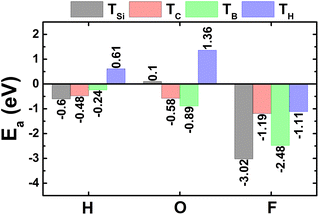
The calculated adsorption energies are given in Fig. 1. Note that TSi is the energetically most favorable adsorption site for H and F atoms with lowest Ea values of −0.60 and −3.02 eV, respectively. Meanwhile, O atom prefers to be adsorbed on top of bridge position with an Ea value of −0.89 eV. Fig. 2a–c shows the relaxed atomic structure of the atom-adsorbed systems, where one can see the buckling height induced around the adsorption sites as consequences of strong interactions between adatoms and their nearest host atoms. The Ab Initio Molecular Dynamic (AIMD) simulations are performed to examine the thermal stability. Results indicate that H-, O-, and F-adsorbed SiC monolayers are thermally stable since no structural destruction is observed at room temperature (300 K) during a large range of time up to 3000 fs (see Fig. S3a–c of the ESI†).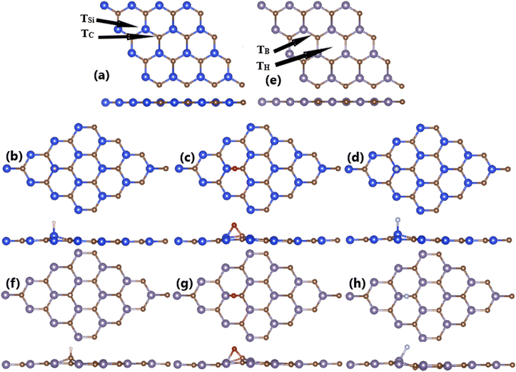 | ||
| Fig. 2 Optimized atomic structure of (a) bare, (b) H-, (c) O-, and (d) F-adsorbed SiC monolayer; and (d) bare, (e) bare, (f) H-, (g) O-, and (h) F-adsorbed GeC monolayer. | ||
Fig. 3 shows the calculated electronic band structures of the atom-adsorbed SiC monolayer. According to our simulations, H adsorption induces a significant spin polarization, giving place to the formation of the magnetic semiconductor nature. Specifically, energy band gaps of 2.58 and 0.03 eV are obtained in the spin-up and spin-down states, respectively. A small spin-down band gap is a result of new flat energy branch above the Fermi level. In contrast, the band structures are spin-symmetric under adsorbing O and F atoms. In the former case, a new middle-gap energy branch appears in the forbidden energy range of SiC monolayer. Consequently, a band gap of 1.88 eV is obtained, which exhibits a reduction of the order of 26% from original value of pristine monolayer (2.54 eV (ref. 61)). Meanwhile, the latter case corroborates the emergence of new electronic states that overlap with the Fermi level and upper part of the valence band. Consequently, the F-adsorbed SiC monolayer exhibits metallic character.
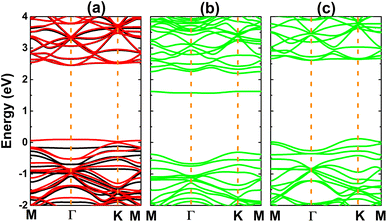 | ||
| Fig. 3 Electronic band structure (the Fermi level is set to 0 eV; black curve: spin-up; red curve: spin-down; green curve: non-spin-polarization) of (a) H-, (b) O-, and (c) F-adsorbed SiC monolayer. | ||
To get insights into the interactions between adatom and host monolayer, the charge density difference Δρ is calculated as follows:
| Δρ = ρ(adatom + SiC) − ρ(SiC) − ρ(adatom) | (2) |
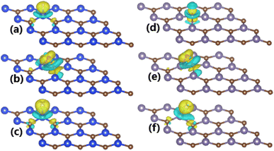
Spin-polarized band structures may suggest the magnetization of SiC induced by adsorbing H atom, meanwhile the non-magnetic nature is preserved under effects of O and F adatoms. Our calculations yield total magnetic moment of 1.00 μB. The illustration of spin density in Fig. 6a indicates that magnetic properties are produced mainly by the spin-up state of H adatom and its nearest C atoms.
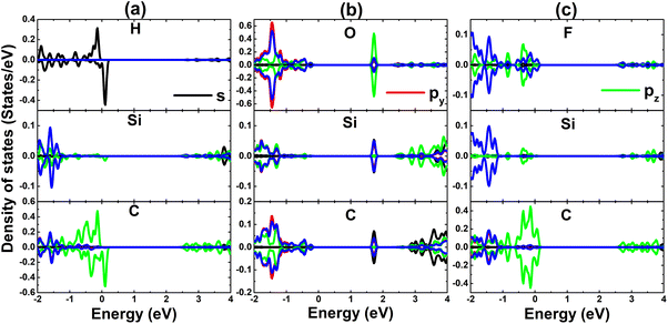 | ||
| Fig. 5 Projected density of state of adatoms and their first Si and C neighbor in (a) H-, (b) O-, and (c) F-adsorbed SiC monolayer. | ||
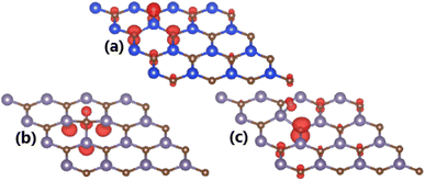 | ||
| Fig. 6 Spin density (red color: spin-up; green color: spin-down; iso-surface: 0.005 e Å−3) in (a) H-adsorbed SiC monolayer; and (b) H- and (c) F-adsorbed GeC monolayer. | ||
Now, to get more insights into the band structure formation and origin of magnetism, the projected density of states (PDOS) spectra are displayed in Fig. 5. It is important mentioning that only PDOS of adatoms and first Si and C neighbor are given considering their important role at the vicinity of the Fermi, which regulate the ground state electronic and magnetic properties of the atom-adsorbed systems. It can be noted that the magnetism of H-adsorbed SiC monolayer is originated from the hybridization between H-s and C-pz states since they exhibit important presence around the Fermi level with a significant spin asymmetry. The charge gaining leads to the emergence of O-px,y and F-px,y,z states in the valence band. However, O-2p orbital is only partially occupied (needing up to two electrons to fulfill 2p orbital), such that O-pz state originates the flat energy branch above the Fermi level to reduce the energy gap, as analyzed above.
B. Atom-adsorbed GeC monolayer
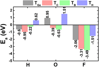
Now, the H, O, and F adsorption on GeC monolayer is investigated. The calculated adsorption energies (given in Fig. 7) suggest TC and TB as preferable adsorption sites for H and O–F atoms with Ea values of −0.95, −0.63, and −3.49 eV, respectively. Remembering that deeply negative adsorption energy is a signal of chemical adsorption, suggesting the stable adsorption of H, O, and F atoms on XC (X = Si and Ge) monolayers. Fig. 2f–h show the relaxed atomic structures, where one can see the structural distortion around the adsorption sites, meanwhile the effects becomes negligible in the regions far away. AIMD simulations assert good thermal stability of the atom-adsorbed GeC monolayers at 300 K (see AIMD snapshots given in Fig. S3d–f of the ESI†).The electronic band structures displayed in Fig. 8 indicate the magnetic semiconductor nature induced by H and F adsorption, meanwhile O adsorption preserves the non-magnetic semiconductor character of GeC monolayer. In all cases, the electronic band gaps are determined by new middle-gap energy branches around the Fermi level. Specifically, spin-up and spin-down energy gaps of the H(F)-adsorbed GeC monolayer are 0.45(2.18) and 1.66(0.06) eV, respectively. In contrast, a same band gap of 1.68 eV is obtained in both spin channels of the O-adsorbed GeC monolayer as consequence of its non-magnetic nature. This value corresponds to a reduction of the order of 18.84% from original value of bare GeC monolayer (2.07 eV (ref. 61)).
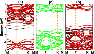 | ||
| Fig. 8 Electronic band structure (the Fermi level is set to 0 eV; black curve: spin-up; red curve: spin-down; green curve: non-spin-polarization) of (a) H-, (b) O-, and (c) F-adsorbed GeC monolayer. | ||
The charge density difference Δρ is calculated using eqn (2) for the cases of GeC monolayer, whose results are illustrated in Fig. 4d–f. Note that the charge is slightly depleted from H adatom with a Bader charge of +0.07 e (“+” signal indicates the charge depletion from adatom). In contrast, significant charge accumulations are observed around O and F adatoms, indicating the charge gaining from host monolayer. Qualitatively, their Bader charges are −0.97 and −0.70 e (“−” signal refers to the charge gaining of adatoms), respectively. Note that the charge transferred to O adatom is larger than to F adatom despite its smaller electronegativity and both adatoms are adsorbed at TB site. The Bader charge analysis of the environment around the adsorption site indicates the important role of both Ge and C host atoms in the case of O adsorption, meanwhile C atom transfers only small amount of charge to F atom. These features can be explained by means of the chemical bond lengths. Specifically, the chemical bonds dO–Ge and dO–C are 1.91 and 1.43 Å, respectively, therefore small distance to the adatom induces important electronic interactions of C host. Meanwhile, the electronic interactions between host monolayer and F adatom are dominated mainly by Ge atom due to the smaller chemical bond length dF–Ge (1.88 Å) in comparison with dF–C (2.58 Å). Consequently, the strong Ge–F interactions lead to an easier adsorption of F adatom than O adatom (regulated mainly by O–C interactions), which is reflected in a more negative adsorption energy as presented above.
The spin-asymmetric band structures may suggest that GeC monolayer has been significantly magnetized by adsorbing H and F atoms, respectively. This feature is reflected in the total magnetic moments of 1 μB in both cases. Remembering that integer total magnetic moment is a characteristic of magnetic materials, which is satisfied in our cases of study. The illustration of spin density is given in Fig. 6b and c to analyze the atomic contribution to magnetic properties. In the H-adsorbed GeC monolayer, magnetism is originated by H adatom and its neighbor C and Si atoms. Meanwhile, main contribution to magnetic properties of the F-adsorbed GeC monolayer comes mainly from first C neighbor of F adatom. In both cases, the spin-up state plays a key role on determining the ground state magnetic properties.
The PDOS spectra, given in Fig. 9, indicates that H adatom induces new middle-gap energy state. In contrast, with significant charge gaining, O and F atoms exhibit electronic states in the valence band (occupied states) and conduction band (unoccupied state), mostly far away from the Fermi level. The hybridization between H-s, Ge-pz, and C-pz states leads to the magnetization in the case of H adsorption. Meanwhile, the C-pz state is the main responsible of generating magnetism in the F-adsorbed GeC monolayer considering its spin asymmetry at the vicinity of the Fermi level.
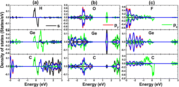 | ||
| Fig. 9 Projected density of state of adatoms and their first Si and C neighbor in (a) H-, (b) O-, and (c) F-adsorbed GeC monolayer. | ||
IV. Conclusions
In summary, the effects of H, O, and F adsorption on the electronic and magnetic properties of XC (X = Si and Ge) monolayers have been investigated using spin-polarized first-principles calculations. The calculated adsorption energies assert that TSi and TB are preferable site for H–F and O adsorption on SiC monolayer. Meanwhile, H and O–F atoms prefer to be adsorbed on top of TC and TB sites of GeC monolayers. Interestingly, the magnetic semiconductor nature is induced in the H-adsorbed SiC monolayer, and H- and F-adsorbed GeC monolayer, which can be used to generate spin current in spintronic devices by means of spin filtering. The spin-dependent band gaps depend on the position of new middle-gap energy branches, which are originated from the electronic hybridization between adatoms and their neighbor atoms. As a characteristic of magnetic semiconductor materials, an integer total magnetic moment of 1 μB. In contrast, the O-adsorbed XC monolayers are non-magnetic, where the energy gaps exhibit significant reduction due to the unoccupied O-pz state. This feature may widen the working region of XC monolayer in optoelectronic devices, endowing them the ability of harvesting more visible light. Moreover, it has been found significant charge transfer from the host monolayer to adatoms, indicating strong interactions between them to generate chemical bonds. Consequently, H, O, and F atoms are chemically adsorbed on XC monolayers, the feature that is also reflected in deeply negative adsorption energies. The findings suggest efficient way to get multifunctional 2D materials from pristine XC monolayer, which could be generalized for other non-magnetic layers.Data availability
The data that support the findings of this study are available from the corresponding author upon request.Computational resources
Calculations were performed in the high-performance computing cluster (HPCC) of Thu Dau Mot University (TDMU) and DGCTIC-UNAM Supercomputing Center (projects LANCAD-UNAM-DGTIC-368).Conflicts of interest
The authors declare that they have no known competing financial interests or personal relationships that could have appeared to influence the work reported in this paper.Acknowledgements
This work is funded by Projects B2023-TNA-06 of the Vietnam Ministry of Education and Training. Dang Tuan Anh would like to extend his gratitude to Thai Nguyen University of Education for the support.References
- K. S. Novoselov, A. K. Geim, S. V. Morozov, D.-e. Jiang, Y. Zhang, S. V. Dubonos, I. V. Grigorieva and A. A. Firsov, Electric field effect in atomically thin carbon films, science, 2004, 306(5696), 666–669 CrossRef CAS PubMed.
- D. R. Cooper, B. D'Anjou, N. Ghattamaneni, B. Harack, M. Hilke, A. Horth, N. Majlis, M. Massicotte, L. Vandsburger, E. Whiteway, et al., Experimental review of graphene, International Scholarly Research Notices, 2012 Search PubMed.
- M. J. Allen, V. C. Tung and R. B. Kaner, Honeycomb carbon: a review of graphene, Chem. Rev., 2010, 110(1), 132–145 CrossRef CAS PubMed.
- C. Soldano, A. Mahmood and E. Dujardin, Production, properties and potential of graphene, Carbon, 2010, 48(8), 2127–2150 CrossRef CAS.
- B. Sensale-Rodriguez, Graphene-based optoelectronics, J. Lightwave Technol., 2015, 33(5), 1100–1108 CAS.
- Y.-B. Chen, J. S. Liu and P. Lin, Recent trend in graphene for optoelectronics, J. Nanopart. Res., 2013, 15, 1–14 Search PubMed.
- Y. Yan, W. I. Shin, H. Chen, S.-M. Lee, S. Manickam, S. Hanson, H. Zhao, E. Lester, T. Wu and C. H. Pang, A recent trend: application of graphene in catalysis, Carbon Letters, 2021, 31, 177–199 CrossRef.
- C. Huang, C. Li and G. Shi, Graphene based catalysts, Energy Environ. Sci., 2012, 5(10), 8848–8868 RSC.
- S. S. Varghese, S. Lonkar, K. Singh, S. Swaminathan and A. Abdala, Recent advances in graphene based gas sensors, Sens. Actuators, B, 2015, 218, 160–183 CrossRef CAS.
- W. Han, R. K. Kawakami, M. Gmitra and J. Fabian, Graphene spintronics, Nat. Nanotechnol., 2014, 9(10), 794–807 CrossRef CAS PubMed.
- P. Seneor, B. Dlubak, M.-B. Martin, A. Anane, H. Jaffres and A. Fert, Spintronics with graphene, MRS Bull., 2012, 37(12), 1245–1254 CrossRef CAS.
- L. Tao, E. Cinquanta, D. Chiappe, C. Grazianetti, M. Fanciulli, M. Dubey, A. Molle and D. Akinwande, Silicene field-effect transistors operating at room temperature, Nat. Nanotechnol., 2015, 10(3), 227–231 CrossRef CAS PubMed.
- J. Zhao, H. Liu, Z. Yu, R. Quhe, S. Zhou, Y. Wang, C. C. Liu, H. Zhong, N. Han and J. Lu, et al., Rise of silicene: a competitive 2D material, Prog. Mater. Sci., 2016, 83, 24–151 CrossRef CAS.
- J. Gou, Q. Zhong, S. Sheng, W. Li, P. Cheng, H. Li, L. Chen and K. Wu, Strained monolayer germanene with 1 × 1 lattice on Sb (111), 2D Materials, 2016, 3(4), 045005 CrossRef.
- M. E. Dávila and G. Le Lay, Few layer epitaxial germanene: a novel two-dimensional Dirac material, Sci. Rep., 2016, 6(1), 1–9 CrossRef PubMed.
- K. F. Mak, M. Y. Sfeir, J. A. Misewich and T. F. Heinz, The evolution of electronic structure in few-layer graphene revealed by optical spectroscopy, Proc. Natl. Acad. Sci. U. S. A., 2010, 107(34), 14999–15004 CrossRef PubMed.
- N. Drummond, V. Zolyomi and V. Fal’Ko, Electrically tunable band gap in silicene, Phys. Rev. B: Condens. Matter Mater. Phys., 2012, 85(7), 075423 CrossRef.
- Z. Ni, Q. Liu, K. Tang, J. Zheng, J. Zhou, R. Qin, Z. Gao, D. Yu and J. Lu, Tunable bandgap in silicene and germanene, Nano Lett., 2012, 12(1), 113–118 CrossRef CAS PubMed.
- Y. Du, J. Zhuang, H. Liu, X. Xu, S. Eilers, K. Wu, P. Cheng, J. Zhao, X. Pi and K. W. See, et al., Tuning the band gap in silicene by oxidation, ACS Nano, 2014, 8(10), 10019–10025 CrossRef CAS PubMed.
- D. Boukhvalov and M. Katsnelson, Tuning the gap in bilayer graphene using chemical functionalization: density functional calculations, Phys. Rev. B: Condens. Matter Mater. Phys., 2008, 78(8), 085413 CrossRef.
- D. Hoat, D. K. Nguyen, R. Ponce-Perez, J. Guerrero-Sanchez, V. Van On, J. Rivas-Silva and G. H. Cocoletzi, Opening the germanene monolayer band gap using halogen atoms: an efficient approach studied by first-principles calculations, Appl. Surf. Sci., 2021, 551, 149318 CrossRef CAS.
- Y.-W. Son, M. L. Cohen and S. G. Louie, Energy gaps in graphene nanoribbons, Phys. Rev. Lett., 2006, 97(21), 216803 CrossRef PubMed.
- M. Y. Han, B. Özyilmaz, Y. Zhang and P. Kim, Energy band-gap engineering of graphene nanoribbons, Phys. Rev. Lett., 2007, 98(20), 206805 CrossRef PubMed.
- S. Mehdi Aghaei and I. Calizo, Band gap tuning of armchair silicene nanoribbons using periodic hexagonal holes, J. Appl. Phys., 2015, 118(10), 104304 CrossRef.
- K. M. McCreary, A. T. Hanbicki, J. T. Robinson, E. Cobas, J. C. Culbertson, A. L. Friedman, G. G. Jernigan and B. T. Jonker, Large-area synthesis of continuous and uniform MoS2 monolayer films on graphene, Adv. Funct. Mater., 2014, 24(41), 6449–6454 CrossRef CAS.
- J. C. Shaw, H. Zhou, Y. Chen, N. O. Weiss, Y. Liu, Y. Huang and X. Duan, Chemical vapor deposition growth of monolayer MoSe2 nanosheets, Nano Res., 2014, 7, 511–517 CrossRef CAS.
- C. Cong, J. Shang, X. Wu, B. Cao, N. Peimyoo, C. Qiu, L. Sun and T. Yu, Synthesis and optical properties of large-area single-crystalline 2D semiconductor WS2 monolayer from chemical vapor deposition, Adv. Opt. Mater., 2014, 2(2), 131–136 CrossRef.
- K. M. McCreary, A. T. Hanbicki, G. G. Jernigan, J. C. Culbertson and B. T. Jonker, Synthesis of large-area WS2 monolayers with exceptional photoluminescence, Sci. Rep., 2016, 6(1), 19159 CrossRef CAS PubMed.
- K. K. Kim, A. Hsu, X. Jia, S. M. Kim, Y. Shi, M. Hofmann, D. Nezich, J. F. Rodriguez-Nieva, M. Dresselhaus and T. Palacios, et al., Synthesis of monolayer hexagonal boron nitride on Cu foil using chemical vapor deposition, Nano Lett., 2012, 12(1), 161–166 CrossRef PubMed.
- J. Zhao, H. Zeng and G. Yao, Computational design of a polymorph for 2D III–V orthorhombic monolayers by first principles calculations: excellent anisotropic, electronic and optical properties, Phys. Chem. Chem. Phys., 2021, 23(6), 3771–3778 RSC.
- H. Şahin, S. Cahangirov, M. Topsakal, E. Bekaroglu, E. Akturk, R. T. Senger and S. Ciraci, Monolayer honeycomb structures of group-IV elements and III-V binary compounds: first-principles calculations, Phys. Rev. B: Condens. Matter Mater. Phys., 2009, 80(15), 155453 CrossRef.
- H. Zheng, X.-B. Li, N.-K. Chen, S.-Y. Xie, W. Q. Tian, Y. Chen, H. Xia, S. Zhang and H.-B. Sun, Monolayer II-VI semiconductors: a first-principles prediction, Phys. Rev. B: Condens. Matter Mater. Phys., 2015, 92(11), 115307 CrossRef.
- H.-F. Lin, W.-M. Lau and J. Zhao, Magnetism in the p-type monolayer II-VI semiconductors SrS and SrSe, Sci. Rep., 2017, 7(1), 45869 CrossRef CAS PubMed.
- M. M. Alyörük, Piezoelectric properties of monolayer II–VI group oxides by first-principles calculations, Phys. Status Solidi B, 2016, 253(12), 2534–2539 CrossRef.
- T.-Y. Lü, X.-X. Liao, H.-Q. Wang and J.-C. Zheng, Tuning the indirect–direct band gap transition of SiC, GeC and SnC monolayer in a graphene-like honeycomb structure by strain engineering: a quasiparticle GW study, J. Mater. Chem., 2012, 22(19), 10062–10068 RSC.
- D. Hoat, M. Naseri, N. N. Hieu, R. Ponce-Pérez, J. Rivas-Silva and G. H. Cocoletzi, Transition from indirect to direct band gap in SiC monolayer by chemical functionalization: a first principles study, Superlattices Microstruct., 2020, 137, 106320 CrossRef CAS.
- C. M. Polley, H. Fedderwitz, T. Balasubramanian, A. A. Zakharov, R. Yakimova, O. Bäcke, J. Ekman, S. P. Dash, S. Kubatkin and S. Lara-Avila, Bottom-Up Growth of Monolayer Honeycomb SiC, Phys. Rev. Lett., 2023, 130, 076203 CrossRef CAS PubMed.
- Z. Xu, Y. Li, C. Li and Z. Liu, Tunable electronic and optical behaviors of two-dimensional germanium carbide, Appl. Surf. Sci., 2016, 367, 19–25 CrossRef CAS.
- L. Drissi, F. Ramadan, H. Ferhati, F. Djeffal and N. B. Kanga, New highly efficient 2D SiC UV-absorbing material with plasmonic light trapping, J. Phys.: Condens. Matter, 2019, 32(2), 025701 CrossRef PubMed.
- F. Ersan, A. G. Gökçe and E. Aktürk, Point defects in hexagonal germanium carbide monolayer: a first-principles calculation, Appl. Surf. Sci., 2016, 389, 1–6 CrossRef CAS.
- E. Bekaroglu, M. Topsakal, S. Cahangirov and S. Ciraci, First-principles study of defects and adatoms in silicon carbide honeycomb structures, Phys. Rev. B: Condens. Matter Mater. Phys., 2010, 81(7), 075433 CrossRef.
- L. Huang, H. Liu, X. Deng and W. Cui, The structural, mechanical and electrical properties of 2D SiC with C-related point defects and substitution of C by foreign atoms, Vacuum, 2023, 208, 111700 CrossRef CAS.
- M. B. Javan, Electronic and magnetic properties of monolayer SiC sheet doped with 3d-transition metals, J. Magn. Magn. Mater., 2016, 401, 656–661 CrossRef.
- X. Fan, J. Jiang, R. Li and W. Mi, Half-metallicity and magnetic anisotropy in transition-metal-atom-doped graphitic germanium carbide (g-GeC) monolayers, J. Phys. Chem. C, 2021, 125(24), 13688–13695 CrossRef CAS.
- Z. Xu, Y. Li, Z. Liu and S. F. Liu, Electronic and magnetic behaviors of B, N, and 3d transition metal substitutions in germanium carbide monolayer, J. Magn. Magn. Mater., 2018, 451, 799–807 CrossRef CAS.
- A. J. Marsden, P. Brommer, J. J. Mudd, M. A. Dyson, R. Cook, M. Asensio, J. Avila, A. Levy, J. Sloan and D. Quigley, et al., Effect of oxygen and nitrogen functionalization on the physical and electronic structure of graphene, Nano Res., 2015, 8, 2620–2635 CrossRef CAS.
- Y. Wang, B. Wang, R. Huang, B. Gao, F. Kong and Q. Zhang, First-principles study of transition-metal atoms adsorption on MoS2 monolayer, Phys. E, 2014, 63, 276–282 CrossRef CAS.
- S.-S. Guan, S.-S. Ke, F.-F. Yu, H.-X. Deng, Y. Guo and H.-F. Lü, Controlling magnetism of monolayer Janus MoSSe by embedding transition-metal atoms, Appl. Surf. Sci., 2019, 496, 143692 CrossRef CAS.
- S. Yadav, B. Agrawal and P. Yadav, Non-magnetic adsorbent functionalized magnetism and spin filtering in a two-dimensional GaN monolayer, J. Phys. Chem. Solids, 2022, 167, 110731 CrossRef CAS.
- X.-F. Ouyang, C.-J. Sun, L. Wang, X. Chang and P. Li, The half-metallicity induced by non-magnetic adatoms on phosphorene nanoribbons, Phys. B, 2023, 648, 414406 CrossRef CAS.
- W. Tang, M. Sun, J. Yu and J.-P. Chou, Magnetism in non-metal atoms adsorbed graphene-like gallium nitride monolayers, Appl. Surf. Sci., 2018, 427, 609–612 CrossRef CAS.
- X. Zhang and Q. Li, Electronic and magnetic properties of nonmetal atoms adsorbed ReS2 monolayers, J. Appl. Phys., 2015, 118(6), 064306 CrossRef.
- J. E. Johns and M. C. Hersam, Atomic covalent functionalization of graphene, Acc. Chem. Res., 2013, 46(1), 77–86 CrossRef CAS PubMed.
- C. Wetzl, A. Silvestri, M. Garrido, H.-L. Hou, A. Criado and M. Prato, The covalent functionalization of surface-supported graphene: an update, Angew. Chem., Int. Ed., 2023, 62(6), e202212857 CrossRef CAS PubMed.
- G. Kresse and J. Furthmüller, Efficiency of ab-initio total energy calculations for metals and semiconductors using a plane-wave basis set, Comput. Mater. Sci., 1996, 6(1), 15–50 CrossRef CAS.
- G. Kresse and J. Furthmüller, Efficient iterative schemes for ab initio total-energy calculations using a plane-wave basis set, Phys. Rev. B: Condens. Matter Mater. Phys., 1996, 54(16), 11169 CrossRef CAS PubMed.
- W. Kohn and L. J. Sham, Self-consistent equations including exchange and correlation effects, Phys. Rev., 1965, 140(4A), A1133 CrossRef.
- J. P. Perdew, K. Burke and M. Ernzerhof, Generalized gradient approximation made simple, Phys. Rev. Lett., 1996, 77(18), 3865 CrossRef CAS PubMed.
- J. Heyd, G. E. Scuseria and M. Ernzerhof, Hybrid functionals based on a screened Coulomb potential, J. Chem. Phys., 2003, 118(18), 8207–8215 CrossRef CAS.
- A. V. Krukau, O. A. Vydrov, A. F. Izmaylov and G. E. Scuseria, Influence of the exchange screening parameter on the performance of screened hybrid functionals, J. Chem. Phys., 2006, 125(22), 224106 CrossRef PubMed.
- C. V. Ha, D. K. Nguyen, D. T. Anh, J. Guerrero-Sanchez and D. Hoat, Novel electronic and magnetic features in XC (X = Si and Ge) monolayers induced by doping with group-VA atoms, New J. Chem., 2023, 47, 2787–2796 RSC.
- H. J. Monkhorst and J. D. Pack, Special points for Brillouin-zone integrations, Phys. Rev. B: Solid State, 1976, 13(12), 5188 CrossRef.
- S. Grimme, J. Antony, S. Ehrlich and H. Krieg, A consistent and accurate ab initio parametrization of density functional dispersion correction (DFT-D) for the 94 elements H-Pu, J. Chem. Phys., 2010, 132(15), 154104 CrossRef PubMed.
- S. Grimme, Semiempirical GGA-type density functional constructed with a long-range dispersion correction, J. Comput. Chem., 2006, 27(15), 1787–1799 CrossRef CAS PubMed.
- J. B. Davis, F. Baletto and R. L. Johnston, The effect of dispersion correction on the adsorption of CO on metallic nanoparticles, J. Phys. Chem. A, 2015, 119(37), 9703–9709 CrossRef CAS PubMed.
- D.-L. Chen, W. Al-Saidi and J. K. Johnson, The role of van der waals interactions in the adsorption of noble gases on metal surfaces, J. Phys.: Condens. Matter, 2012, 24(42), 424211 CrossRef PubMed.
Footnote |
| † Electronic supplementary information (ESI) available. See DOI: https://doi.org/10.1039/d3ra01372c |
| This journal is © The Royal Society of Chemistry 2023 |

