
 Open Access Article
 This Open Access Article is licensed under a Creative Commons Attribution-Non Commercial 3.0 Unported Licence
Modeling the path to >30% power conversion efficiency in perovskite solar cells with plasmonic nanoparticles†
Md. Mashrafia,
M. Hussayeen Khan Anikb,
Mst. Farhana Isratac,
Ahsan Habiba and
Sharnali Islam *ac
*ac
aDepartment of Electrical and Electronic Engineering, University of Dhaka, 1000, Dhaka, Bangladesh. E-mail: sharnali.eee@du.ac.bd
bDepartment of Electrical and Electronic Engineering, Shahjalal University of Science and Technology, 3114, Sylhet, Bangladesh
cSemiconductor Technology Research Centre, University of Dhaka, Bangladesh
First published on 27th June 2023
Abstract
Mixed organic–inorganic halide perovskite solar cells (PSCs) are a promising technology with increasing power conversion efficiency (PCE), low-cost material constituents, simple scalability, and a low-temperature solution fabrication process. Recent developments have seen energy conversion efficiencies increase from 3.8% to over 20%. However, to further improve PCE and reach the target efficiency of over 30%, light absorption through plasmonic nanostructures is a promising approach. In this work, we present a thorough quantitative analysis of the absorption spectrum of a methylammonium lead iodide (CH3NH3PbI3) perovskite solar cell using a nanoparticle (NP) array. Our multiphysics simulations using finite element methods (FEM) show that an array of Au nanospheres can increase average absorption >45%, compared to only 27.08% for the baseline structure without any NPs. Furthermore, we investigate the combined effect of engineered enhanced absorption on electrical and optical solar cell performance parameters using the one-dimensional solar cell capacitance software (SCAPS 1-D), which shows a PCE of ∼30.4%, significantly higher than the PCE of ∼21% for cells without NPs. Our findings demonstrate the potential of plasmonic perovskite research for next-generation optoelectronic technologies.
1 Introduction
Over the last two decades, the demand for renewable energy sources has been gradually increasing worldwide.1,2 Among these sources, solar energy is considered the most abundant, clean, and environmentally friendly.3,4 By harnessing the “photovoltaic effect”, solar cells can directly convert sunlight into electrical energy, enabling large-scale power generation.5 In 2021, a record-breaking 168 GW of solar energy was generated, laying the groundwork for 1 TW of solar energy by 2030. While traditional silicon solar cells have numerous benefits, such as their established technology and proven reliability, there is a growing need for new technologies with greater energy conversion efficiency or lower processing costs. A promising candidate for such a technology is a new class of hybrid organic–inorganic halide perovskites (PSCs).6,7 These materials have shown remarkable potential in both aspects, with PSCs achieving a power conversion efficiency (PCE) of over 23.3% for a small-area device (9 mm2).8 However, this efficiency is much lower than that of silicon solar cells (150 mm2).9 The main reason for this low efficiency is the issue of poor longer-wavelength photon capture, which must be addressed to further enhance the performance of PSCs.10,11The field of plasmonics has emerged as a promising avenue to enhance the performance of photovoltaic devices, including PSCs.12,13 Plasmonics refers to the interaction between light and free electrons in metals, which results in the excitation of surface plasmons at specific resonance wavelengths.14 Plasmonic nanostructures, such as nanoparticles made of gold or silver, have shown great potential in enhancing the absorption of light in solar cells.15,16 This is achieved through two mechanisms: (i) by exciting localized surface plasmon resonances that couple and trap incoming sunlight into a thin absorber layer, and (ii) by acting as antennas at optical frequencies, where the plasmonic near-field is coupled to the solar material, thereby increasing its effective absorption cross-section. In addition, plasmonic nanoparticles scatter incoming light into dielectric-like waveguide modes of the solar cell, increasing the average light path length within the solar cells.17 These effects result in a significant enhancement of the light–matter interaction and, consequently, an increase in the photocurrent density.18 Therefore, plasmonics is a promising approach to address the issue of poor longer-wavelength photon capture in PSCs and holds great potential for further improving their efficiency.
In this study, we present an approach for enhancing the efficiency of PSCs by incorporating an array of plasmonic nanoparticles (NPs) into the perovskite absorber layer. Our approach aims to increase the light absorption of the cell without altering its typical configuration or the geometry of its components, which is essential for maintaining efficiency. By exciting plasmonic modes and enhancing light scattering, the array of NPs increases the absorption of the perovskite layer. To investigate the mechanism of absorption enhancement, we use multiphysics modeling and finite element techniques. Our results demonstrate that using arrayed NPs can improve the average absorption of the perovskite layer by up to 14% across the wavelength range of 300 nm to 2000 nm. Furthermore, we analyze the influence of nanoparticle size and spacing on the absorption enhancement and find that shrinking the spacing can lead to a considerable improvement of up to 45% due to the high near-field coupling. To comprehensively assess the impact of plasmonic nanostructures on cell performance, we evaluate measures such as open-circuit voltage (VOC), short circuit current density (JSC), fill factor (FF), and power conversion efficiency (PCE) using the one-dimensional solar cell capacitance program (SCAPS 1-D). Our results show that incorporating arrayed NPs into the cell increases the short circuit current density from 26.63 mA cm−2 to 39.40 mA cm−2 and improves the PCE from 21.77% to 30.4%, when compared with the baseline counterpart (without any NPs). Additionally, we investigate the effect of employing different materials, with the highest absorption and PCE observed for Au NPs. Our findings suggest that the incorporation of plasmonic nanoparticles into perovskite solar cells offers a promising strategy for enhancing their efficiency and performance.
2 Methodology
The proposed perovskite solar cells, illustrated in Fig. 1, comprise five layers arranged in the following order: Ag serves as the back contact, p-type P3HT functions as the hole transporting layer (HTL), methylammonium lead iodide (CH3NH3PbI3) perovskite acts as the absorber layer, n-type TiO2 serves as the electron transporting layer (ETL), and indium tin oxide (ITO) is used as a transparent conducting oxide. A layer of glass sits on top of the device. Fig. 1 shows an array of nine nanospheres arranged in a 3 × 3 pattern embedded in the absorber layer. The thicknesses of each layer are provided in Table 1.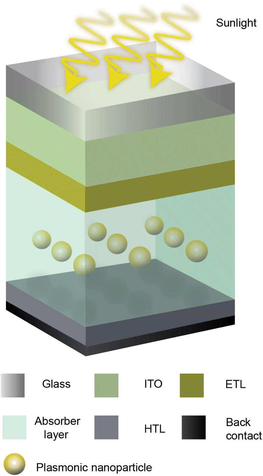 | ||
| Fig. 1 Schematic illustrations of perovskite solar cells. Light from the top illuminates a transparent glass layer followed by an indium tin oxide (ITO) layer, an electron transport layer (ETL), a perovskite absorber layer, a hole transport layer (HTL), and a back contact. The structure with a plasmonic nanosphere array for enhanced performance is added to the perovskite absorber layer, resulting in localized surface plasmon resonance that enhances light absorption and increases photocurrent. The diameter and spacing of the nanospheres can be adjusted to optimize device performance. | ||
| Layer name | Material | Thickness (nm) |
|---|---|---|
| Glass cover | Soda-lime glass | 40 |
| Transparent conducting oxide | ITO | 40 |
| n-type ETL | TiO2 | 10 |
| Perovskite layer | CH3NH3PbI3 | 400 |
| p-type HTL | P3HT | 40 |
| Metal contact | Ag | 40 |
In this work, a three-dimensional optical simulation was carried out using the finite element method (FEM) in COMSOL Multiphysics. The FEM is a numerical technique used to solve partial differential equations for boundary value problems. For optical simulations, Maxwell's equations in the frequency domain were solved initially, given as:
| ∇ × (∇ × E) − ε0k0E = 0 | (1) |
| ε(λ) = (n(λ) + ik(λ))2 | (2) |
In order to benchmark and validate our simulation methodology, we performed a comprehensive analysis and comparison of our simulated results with available experimental data (ESI text ST1†). Specifically, we conducted a detailed investigation of the optical properties of a single silver nanoparticle exposed to different solvent environments, as reported by McFarland et al.21 By simulating the optical intensity and comparing it with the experimental findings, we successfully validated our electromagnetic simulations. Our calculated intensity exhibited excellent agreement with the experimental data (ESI Fig. S1†). The resonant peak was observed at the same wavelength as the experimental findings, further confirming the accuracy of our simulation approach.
3 Results and discussion
3.1 Effects of introducing plasmonic nanoparticles
We analyze the optical absorption of a planar perovskite solar cell (PSC) to determine how embedded nanoparticles impact absorption rates and whether this can enhance the cell's power conversion efficiency (PCE). We implement a proposed nanoparticle structure on the PSC to achieve this goal. First, we calibrate the baseline PSC structure (without nanoparticles) against existing literature.22 Fig. 2 shows that our results (yellow dash line) align with previous research (black dotted line). The ultraviolet and visible light ranges exhibit high absorption rates, reaching a peak of 0.96 at 720 nm. However, the extinction coefficient value drops to nearly zero in the infrared region, leading to a significant decrease in absorption rates.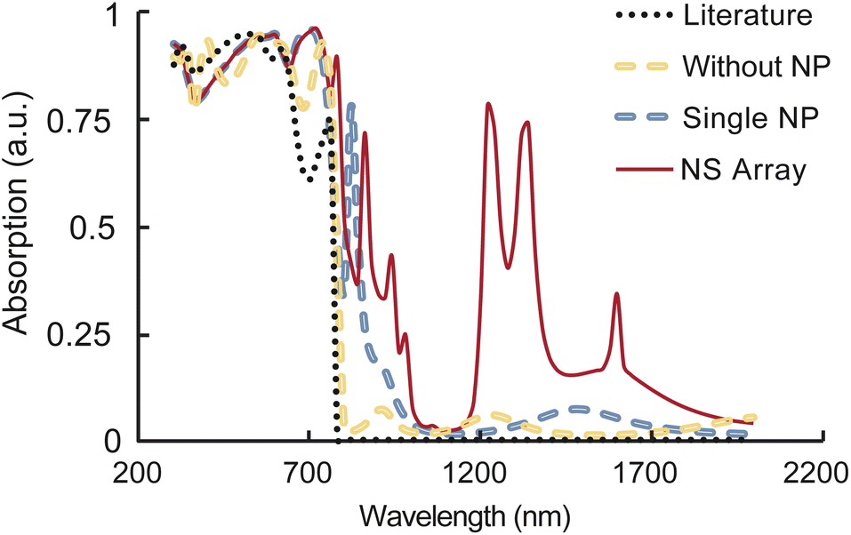 | ||
| Fig. 2 Comparison of the absorption spectrum in the perovskite layer of the proposed structures, including no nanoparticles, a single 80 nm-diameter Au nanosphere, and a 3 × 3 array of nanospheres (spacing 5 nm). The addition of the 3 × 3 array enhances IR absorption rates, with distinct peaks at 1220 nm and 1340 nm. The black dotted line in the figure represents the comparison of our baseline structure, without any nanoparticles, with the results reported in the existing literature.22 This comparison indicates that our results are in good agreement with prior research. | ||
The addition of plasmonic nanospheres to the perovskite layer significantly improves the absorption and photocurrent of the solar cell. When a single 80 nm-diameter Au nanosphere is added to the center of the perovskite layer, a new absorption peak appears around 820 nm (Fig. 2). Replacing the single particle with a 3 × 3 array of nanospheres (spacing 5 nm) further boosts the infrared region, resulting in two distinct absorption peaks at 1220 nm and 1340 nm. We choose a 3 × 3 array size to demonstrate the feasibility and potential benefits of integrating nanospheres into the perovskite layer and also based on our computational resources. To explore the influence of several other array forms on the potential benefits of integrating nanospheres, different sizes of arrays are simulated and results are shown in, Fig. S3 and S4.† We observed that after a 3 × 3 array, the absorption doesn't increase considerably, justifying our array size selection. We have also investigated the optimum distance between the nanosphere and the sidewall. The distance between the sidewall and the center of the closest particle lS has been considered as a multiple of d, where d is the diameter of the nanoparticle, s is the distance between the two closest particles (Fig S5†). We have observed average absorption of 0.3812, 0.3979, 0.4179, 0.4153, 0.4127 for the distance of 1.8 × d, 2 × d, 2.3 × d, 2.5 × d and 3 × d respectively. We have found that after 2.3 × d, absorption does not depend much on the distance. So in our study, we use this value to form the unit cell.
Compared to the base structure with an average absorption of 27.08% over the wavelength range of 300 nm to 2000 nm, the addition of a single nanosphere increases the average absorption of the perovskite layer to 30.41%, while the nanosphere array increases it to 41.79%. The average absorption attributable to the plasmonic nanoparticles was calculated using the trapezoidal method. This indicates that the nanosphere array is responsible for the significant improvement of nearly 14%. The compact packing of plasmonic materials in the nanosphere array enhances the near-field effect for plasmonic behavior, leading to increased absorption of photons and the generation of more electron–hole pairs.
The absorption enhancement due to the embedded nano-sphere array can be understood by analyzing the electric field profile. Fig. 3a and b depict nanospheres with a diameter of 80 nm placed at distances of 5 nm and 20 nm, respectively, to demonstrate the increase in absorption. As the distance between the spheres decreases, the perovskite layer experiences strong light absorption due to the coupling effect, as shown in Fig. 3a. In plasmonics, the coupling effect refers to the interaction between the plasmon modes of two or more metal nanoparticles or other plasmonic structures.23 When two or more plasmonic structures are brought into close proximity, the plasmon modes of each structure can interact with each other, leading to a range of interesting and useful optical effects. This strong coupling effect is a result of the strong field coupling between the nanospheres and the perovskite layer. However, as the distance between the nanospheres increases, the coupling effect diminishes, as illustrated in Fig. 3b.
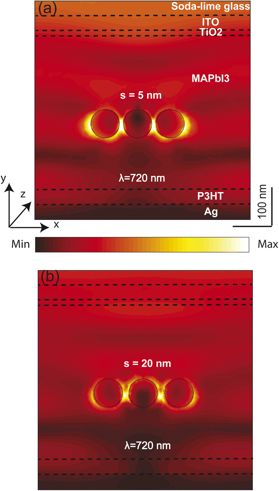 | ||
| Fig. 3 Electric field profile for a single nanosphere with a diameter of 80 nm, illuminated by light with a wavelength of 720 nm, placed at two different distances: (a) 5 nm and (b) 20 nm. The color map shows the magnitude of the electric field intensity, with white representing the highest intensity and black the lowest. The strong coupling effect between the nanosphere and the incident light is observed at a smaller distance (a), while the coupling effect diminishes as the distance between the nanosphere and the light source increases (b). The electric field profile is obtained using the software COMSOL Multiphysics. The software uses finite element method (FEM) to solve the equations governing the interaction of light with nanospheres and other materials, providing a detailed analysis of the electric field intensity and distribution around the nanostructure. | ||
Mathematically, the electric field profile can be expressed using the following equation:24
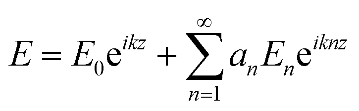 | (3) |
The absorption enhancement is attributed to the excitation of surface plasmon resonances (SPRs) in the nanospheres, which couple with the perovskite layer. The coupling effect is maximized when the SPR frequency of the nanospheres matches the frequency of the incident light, leading to the formation of hot spots with high field intensity. These hot spots increase the local density of optical states, leading to a higher probability of photon absorption by the perovskite layer.
Nanoparticle size plays a crucial role in determining coupling efficiency. In this study, we investigate the influence of nanoparticle diameter variation on the absorption spectrum. Fig. 4a shows the results for a single layer of a 3 × 3 array of nanospheres with diameters of 20 nm, 50 nm, and 80 nm, with a constant spacing of 5 nm for fair comparison. The red dashed line represents the absorption spectrum for the case without any nanoparticles as reference.
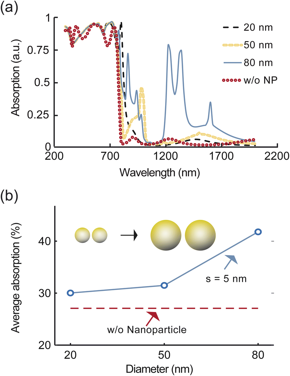 | ||
| Fig. 4 Effect of varying the diameter of nanospheres on the absorption spectrum of the active layer. (a) Displays the absorption spectrum of a 3 × 3 array of nanospheres with diameters of 20 nm, 50 nm, and 80 nm, as well as a reference spectrum without any nanoparticles. The results show that increasing the diameter of the nanospheres leads to a clear right shift of the absorption peak, consistent with Mie theory. Furthermore, the amount of light trapping in the solar cell increases with increasing diameter, resulting in more light absorption. (b) Depicts the total absorption flux for different nanosphere diameters ranging from 20 nm to 80 nm at a fixed spacing of 5 nm, and a reference line for without any nanoparticles. The results demonstrate a more than 10% enhancement in absorbance due to strongly scattered far-field, highlighting the critical role of nanoparticle size in determining coupling efficiency. | ||
Compared to the no nanoparticle case, the introduction of a 20 nm nanoparticle leads to the appearance of small absorption peaks around a wavelength of 780 nm. For larger nanoparticle diameters, a clear red shift of the absorption peak is observed, in agreement with the Mie theory, which predicts that the absorption peak shifts towards longer wavelengths with increasing nanoparticle diameter. This trend is observed in all our results. As the nanoparticle diameter increases, the amount of light trapping also increases due to enhanced scattering.25 This increased light trapping results in more light being absorbed in the solar cell.
Fig. 4b shows the influence of nanoparticle diameter variation on the increase of perovskite solar cell absorption. By varying the diameter of the nanospheres from 20 nm to 80 nm for a fixed spacing of 5 nm, we observe an enhancement in average absorption of more than 14% due to strongly scattered far-field.26,27
Fig. 5a illustrates the impact of spacing variations between nanospheres with a diameter of d = 80 nm on the absorption spectrum of the perovskite layer. As the spheres are brought closer together, light confinement increases among the nanospheres. The broadest peak with the highest average absorption of approximately 45% is observed for the smallest spacing of s = 2 nm. However, for s = 5 nm and 10 nm, the average absorption decreases to 41% and 36%, respectively. Fig. 5b shows the variation of spacing while keeping the diameter fixed at d = 80 nm. The absorption of light significantly increases as the spacing decreases, with maximum absorption occurring at s = 2 nm. This is attributed to the strong near-field coupling.27
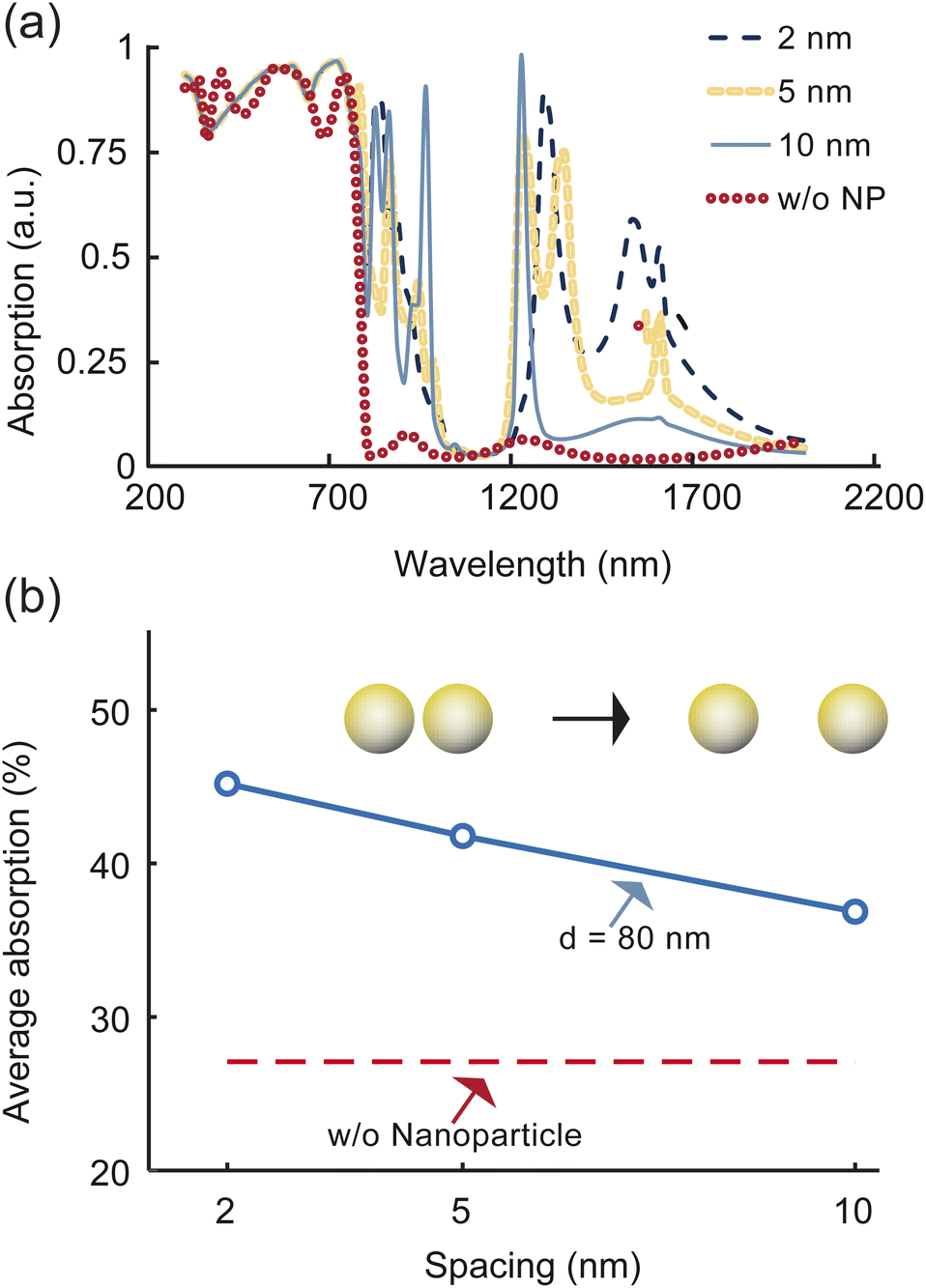 | ||
| Fig. 5 Effect of spacing variation between nanospheres in the absorption spectrum of the perovskite layer. (a) Changes in the absorption spectrum for varying spacing values while keeping the diameter fixed at d = 80 nm. As the spheres are brought closer together, light confinement increases among the nanospheres. The broadest peak with the highest average absorption of approximately 46% is observed for the smallest spacing of s = 2 nm. However, for s = 5 nm and 10 nm, the average absorption decreases to 43% and 40%, respectively. (b) Average absorption for different spacing values while maintaining the diameter at a fixed value, along with a reference line for the baseline structure. The absorption of light significantly increases as the spacing decreases, with maximum absorption occurring at s = 2 nm, attributed to the strong near-field coupling. | ||
In this study, we investigate the impact of plasmonic nanostructures on the performance parameters of solar cells. Specifically, we analyze the open-circuit voltage (VOC), short circuit current density (JSC), fill factor (FF), and power conversion efficiency (η) using the one-dimensional solar cell capacitance program (SCAPS 1-D). This tool solves Poisson's equation and the continuity equations for carrier calculations, using material properties adopted from the literature. All material properties used in this study are taken from previously published literature sources28,29 (ESI Table S2†). In our study, the addition of the nanoarray is achieved through a two-step simulation approach (ESI Fig. S6†). First, we utilize FEM-based COMSOL software to solve the Maxwell equations and obtain the absorption profile of the solar cell. The absorption profile is then imported into the Solar Cell Capacitance Simulator (SCAPS-1D) software, which allows us to simulate the electrical response of the cell. To validate our simulation results, we rely on a combination of experimental data and previous studies (ESI text ST3†). Specifically, we select a published study30 that utilizes methylammonium-free perovskite solar devices based on the formamidinium organic cation. This study provides UV-visible spectroscopic absorption curves and SCAPS-generated I–V characteristics for various absorber layers. By incorporating the thickness, refractive index, and other optical data from this study into our COMSOL model, we are able to reproduce the absorption curve, as shown in ESI Fig. S7a.†
To evaluate the effect of plasmonic nanostructures, we first simulate a baseline structure using the absorption spectrum calculated for no nanosphere (shown as a red dashed line in Fig. 5a). We then simulate the impact of 3 × 3 array of nanospheres using our absorption data (shown as a black dashed line in Fig. 5a) obtained from FEM analysis. The comparison of the performance matrices of PSCs is shown in Table 2.
| Structure | VOC (V) | JSC (mA cm−2) | FF (%) | η (%) |
|---|---|---|---|---|
| No NPs | 1.14 | 26.63 | 71.5 | 21.77 |
| With NPs | 1.15 | 39.42 | 70.05 | 30.4 |
Fig. 6 depicts the relationship between the performance metrics of the plasmonic solar cell and the diameter and spacing of the plasmonic nanospheres. Our FEM simulation predicted that the highest current density would be obtained when the nanospheres had the largest diameter and were closest to one another, which is supported by the data shown in Fig. 6a. Specifically, the highest current density (JSC) of 39.40 mA cm−2 is achieved when the diameter of the nanospheres (d) is 80 nm and the spacing between them (s) is 2 nm.
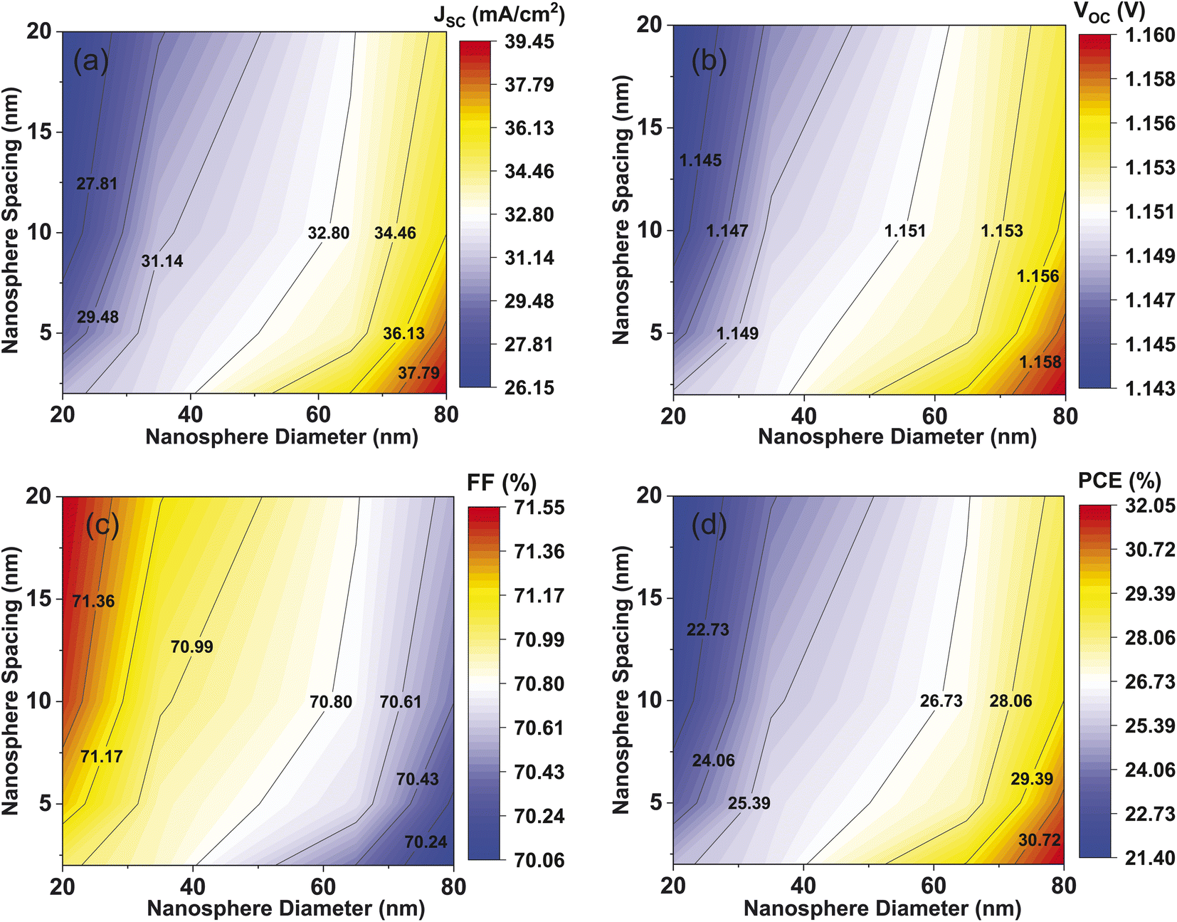 | ||
| Fig. 6 A comprehensive electrical analysis of the impact of nanoparticle diameter and spacing on the performance characteristics of plasmonic nanoparticle-containing perovskite solar cells. Panel (a) displays the current density (JSC) variation with nanoparticle diameter and spacing. The data in panel (a) support our FEM simulation, which predicted that the highest current density of 39.40 mA cm−2 would be achieved when the nanoparticle diameter (d) is 80 nm and the spacing (s) is 2 nm. Panel (b) demonstrates that increasing the diameter of the nanoparticles and reducing the spacing between them slightly enhances the open-circuit voltage (VOC). Panel (c) presents the fill factor (FF) as a function of nanoparticle diameter and spacing, which shows that FF decreases slightly as nanoparticle diameter increases and spacing between the nanoparticles decreases. Panel (d) is a contour plot of PCE as a function of both nanoparticle diameter and spacing, which provides a comprehensive evaluation of the influence of these parameters on the performance of solar cells. | ||
In Fig. 6b, it is evident that increasing the diameter of the nanospheres while decreasing the distance between them slightly enhances the open-circuit voltage (VOC). Moreover, as shown in Fig. 6c, the fill factor (FF) decreases somewhat as the diameter of the nanoparticle increases and the distance between the nanoparticles decreases. The contour plot of PCE as a function of both nanoparticle spacing and diameter is shown in Fig. 6d. For a solar cell, PCE can be calculated as follows:
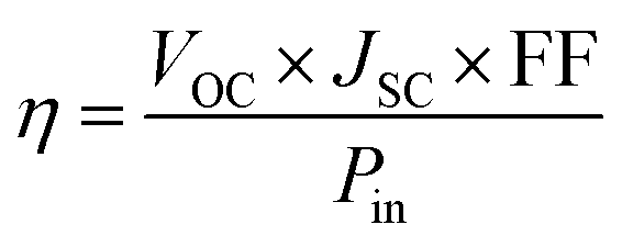 | (4) |
In this study, the impact of different materials, namely Au, Ag, ITO, and TiO2, on the absorption spectrum of a single layer of nanospheres (as illustrated in Fig. 1) for perovskite solar cells is examined, as depicted in Fig. 7a. The results show that the average absorption, reaching 42%, is obtained with Au nanomaterials, as shown in Fig. 7b. Ag nanoparticles has a slightly lower average absorption compared to Au, while ITO and TiO2 exhibit the lowest absorption of approximately 28% and 27% respectively. The J–V curve demonstrates a similar trend to that observed in the absorption spectrum, with the maximum current density achieved for the gold and silver nanomaterials, as shown in Fig. 7c. Additionally, the power conversion efficiency of the perovskite solar cell, as shown in Fig. 7d, is highest at 30.4% for Au nanospheres, while the lowest power conversion efficiency was found for ITO and TiO2 at approximately 22%.
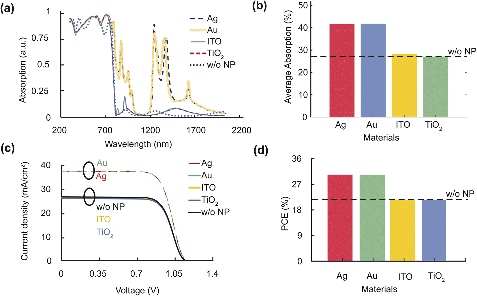 | ||
| Fig. 7 The impact of various nanomaterials, including Au, Ag, ITO, and TiO2, on the absorption spectrum of a perovskite layer, as well as the J–V curve and efficiency of the corresponding solar cells. (a) The absorption spectrum for each material and a baseline structure with no particles, revealing that Au nanomaterials exhibit the highest average absorption of 42%, while ITO and TiO2 have the lowest absorption of approximately 28%, and 27% respectively. (b) The average absorption of each material. (c) The J–V curve for each material, with the highest current density achieved for gold and silver nanomaterials. (d) The power conversion efficiency for each material, with Au nanospheres exhibiting the highest efficiency of 30.4%, while ITO and TiO2 have the lowest efficiency at approximately 22%. | ||
4 Conclusions
In this work, we have investigated the use of plasmonic nanoparticles as efficient light absorbers to enhance the light-harvesting of perovskite solar cells in the IR region. Specifically, we have studied the effect of an Au nanosphere array buried in the perovskite layer, and have optimized the diameter and spacing of the nanospheres for maximum efficiency. Using our finite element calculation, we found that a larger diameter of d = 80 nm (s = 5 nm) and the lowest spacing of 2 nm (with d = 80 nm) resulted in the maximum absorption of 46%.We also reported the electrical parameters, such as VOC, JSC, FF, and PCE, and compared the results with the base structure (no nanoparticle). Due to the closely spaced nanospheres, light trapping increased, and we achieved a maximum current density of JSC = 39.40 mA cm−2. Similarly, the highest PCE (30.4%) was obtained for the largest d and the lowest s between the nanospheres, showing a 40% enhancement compared to the baseline structure.
We then investigated different types of plasmonic materials and found that Au was the best for its high absorption capability. In summary, adding a nanosphere array into the perovskite layer is an efficient way to improve light absorption in the IR region, as well as increase JSC and PCE.
Author contributions
M. Mashrafi, M. F. Israt, and M. H. K. Anik planned and carried out the simulations, performed data analysis, and drafted the initial manuscript. A. Habib supervised, provided significant suggestions on technical content, and reviewed the writing. S. Islam conceptualize the project, supervised, coordinated the research, and reviewed the writing. All the authors edited and approved the manuscript.Conflicts of interest
There are no conflicts to declare.Acknowledgements
We would like to express their sincere appreciation to Nishat Tasnim for her invaluable contribution in drawing the schematic illustration for this study. Her expertise and dedication have greatly enhanced the visual presentation of our findings, and we are grateful for her hard work and commitment to this project. Furthermore, we would like to thank the technical support from Fab Lab DU and Semiconductor Technology Research Centre at the University of Dhaka, and Bangladesh Research and Education Network (BdREN) for providing the necessary computational resources for this simulation study. Their assistance was crucial in carrying out the simulations and analyzing the data, and we are grateful for their support.Notes and references
- F. Egli, B. Steffen and T. S. Schmidt, Nat. Energy, 2018, 3, 1084–1092 CrossRef.
- D. Gielen, F. Boshell, D. Saygin, M. D. Bazilian, N. Wagner and R. Gorini, Energy Strategy Rev., 2019, 24, 38–50 CrossRef.
- N. Kannan and D. Vakeesan, Renewable Sustainable Energy Rev., 2016, 62, 1092–1105 CrossRef.
- J. Khan and M. H. Arsalan, Renewable Sustainable Energy Rev., 2016, 55, 414–425 CrossRef.
- A. Polman, M. Knight, E. C. Garnett, B. Ehrler and W. C. Sinke, Science, 2016, 352(6283), 1–10 CrossRef PubMed.
- M. A. Green, A. Ho-Baillie and H. J. Snaith, Nat. Photonics, 2014, 8, 506–514 CrossRef CAS.
- M. A. Alkhalayfeh, A. A. Aziz, M. Z. Pakhuruddin and K. M. M. Katubi, Phys. Status Solidi A, 2021, 218, 2100310 CrossRef CAS.
- Y. Rong, Y. Hu, A. Mei, H. Tan, M. I. Saidaminov, S. I. Seok, M. D. McGehee, E. H. Sargent and H. Han, Science, 2018, 361, 1–7 CrossRef PubMed.
- I.-K. Ding, J. Zhu, W. Cai, S.-J. Moon, N. Cai, P. Wang, S. M. Zakeeruddin, M. Grätzel, M. L. Brongersma and Y. Cui, et al., Adv. Energy Mater., 2011, 1, 52–57 CrossRef CAS.
- H.-J. Du, W.-C. Wang and J.-Z. Zhu, Chin. Phys. B, 2016, 25, 108802 CrossRef.
- N. Moshonas, N. A. Stathopoulos and G. Pagiatakis, Electronics, 2022, 11, 2041 CrossRef CAS.
- G. Kakavelakis, K. Petridis and E. Kymakis, J. Mater. Chem. A, 2017, 5, 21604–21624 RSC.
- R. Siavash Moakhar, S. Gholipour, S. Masudy-Panah, A. Seza, A. Mehdikhani, N. Riahi-Noori, S. Tafazoli, N. Timasi, Y.-F. Lim and M. Saliba, Adv. Sci., 2020, 7, 1902448 CrossRef CAS PubMed.
- J. A. Dionne, L. A. Sweatlock, H. A. Atwater and A. Polman, Phys. Rev. B, 2005, 72(7), 1–11 CrossRef.
- Q. Rehman, A. D. Khan, A. D. Khan, M. Noman, H. Ali, A. Rauf and M. S. Ahmad, RSC Adv., 2019, 9, 34207–34213 RSC.
- H. A. Atwater and A. Polman, Nat. Mater., 2010, 9, 865 CrossRef CAS.
- W. Yan, Y. Liu, Y. Zang, J. Cheng, Y. Wang, L. Chu, X. Tan, L. Liu, P. Zhou, W. Li and Z. Zhong, Nano Energy, 2022, 99, 107394 CrossRef CAS.
- M. Seyyedi and H. Heidarzadeh, Opt. Mater., 2023, 135, 113287 CrossRef CAS.
- P. B. Johnson and R. W. Christy, Phys. Rev. B, 1972, 6, 4370–4379 CrossRef CAS.
- J. M. Ball, S. D. Stranks, M. T. Hörantner, S. Hüttner, W. Zhang, E. J. W. Crossland, I. Ramirez, M. Riede, M. B. Johnston, R. H. Friend and H. J. Snaith, Energy Environ. Sci., 2015, 8, 602–609 RSC.
- A. D. McFarland and R. P. V. Duyne, Nano Lett., 2003, 3, 1057–1062 CrossRef CAS.
- L. Yue, B. Yan, M. Attridge and Z. Wang, Sol. Energy, 2016, 124, 143–152 CrossRef CAS.
- M. Kim, H. Kwon, S. Lee and S. Yoon, ACS Nano, 2019, 13, 12100–12108 CrossRef CAS PubMed.
- C. F. Bohren and D. R. Huffman, Absorption and scattering of light by small particles, John Wiley & Sons, 2008 Search PubMed.
- M. A. Alkhalayfeh, A. A. Aziz and M. Z. Pakhuruddin, Renewable Sustainable Energy Rev., 2021, 141, 110726 CrossRef CAS.
- M. Terakawa, S. Takeda, Y. Tanaka, G. Obara, T. Miyanishi, T. Sakai, T. Sumiyoshi, H. Sekita, M. Hasegawa, P. Viktorovitch and M. Obara, Prog. Quantum Electron., 2012, 36, 194–271 CrossRef.
- V. G. Kravets, A. V. Kabashin, W. L. Barnes and A. N. Grigorenko, Chem. Rev., 2018, 118, 5912–5951 CrossRef CAS PubMed.
- B. Farhadi, M. Ciprian, F. Zabihi and A. Liu, Sol. Energy, 2021, 226, 161–172 CrossRef CAS.
- Y. Raoui, H. Ez-Zahraouy, N. Tahiri, O. E. Bounagui, S. Ahmad and S. Kazim, Sol. Energy, 2019, 193, 948–955 CrossRef CAS.
- S. Karthick, S. Velumani and J. Bouclé, Sol. Energy, 2020, 205, 349–357 CrossRef CAS.
Footnote |
| † Electronic supplementary information (ESI) available. See DOI: https://doi.org/10.1039/d3ra02589f |
| This journal is © The Royal Society of Chemistry 2023 |