 Open Access Article
Creative Commons Attribution 3.0 Unported Licence
First principles investigation of halide based Rb2NaGaZ6 (Z = Br, I) double perovskites for energy harvesting applications
Huda A. Alburaiha,
Ghulam M. Mustafa *b,
Pakeeza Aymen Nawazc,
Sadaf Sabad,
N. A. Noor
 e,
Asif Mahmoodf and
Ramesh Sharma
 g
g
aDepartment of Physics, College of Science, Princess Nourah Bint Abdulrahman University, P.O. Box 84428, Riyadh 11671, Saudi Arabia
bDepartment of Physics, Division of Science and Technology, University of Education, Lahore, Punjab 54770, Pakistan. E-mail: dr.ghulam.muhammad@ue.edu.pk
cDepartment of Physics, University of Lahore, Lahore, Pakistan
dCenter of Excellence in Solid State Physics, University of the Punjab, Lahore, Pakistan
eDepartment of Physics, RIPHAH International University, Campus Lahore, Pakistan
fChemical Engineering Department, College of Engineering, King Saud University, Riyadh, Saudi Arabia
gDept. of Applied Science, Feroze Gandhi Institute of Engineering and Technology, Raebareli, 229001, Uttarpradesh, India
First published on 8th December 2023
Abstract
Extensive investigations have been conducted on the thermoelectric and optoelectronic characteristics of double perovskite compounds using the full potential linearized augmented plane wave (FP-LAPW) approach. Here we investigated Rb2NaGaZ6 (Z = Br, I) to explore its band structure, and electronic, optical and transport properties. Born's stability criteria have confirmed the mechanical stability of these compounds. Analysis of the elastic properties reveals their ductile nature, as indicated by a Poisson coefficient (υ) greater than 0.26 and a Pugh ratio exceeding 1.75 for Rb2NaGaZ6 (Z = Br, I). Computation of the bandgap values shows that both compositions possess a direct bandgap nature, with respective values of 2.90 eV and 1.25 eV. This suggests that substituting Br with I brings the band edges closer together, resulting in a decrease in the bandgap value. The optical properties are assessed based on the absorption coefficient, reflectivity, and dielectric constants. The thermoelectric properties, including thermal and electrical conductivities, power factor (PF), and figure of merit (ZT), are determined using the BoltzTrap code. The ZT values indicate that both compositions exhibit promising potential for various transportation applications.
1. Introduction
In the era of constant technological evolution and expansion in economic advancement, to save time, effort, and energy for development we are dependent on machines, which results in environmental degradation.1–4 At the moment, to attain this energy demand, on a large scale, fossil fuels are being utilized which is consequently giving rise to environmental pollution and climate change. Therefore, to solve this issue renewable energy sources are required,9,10 like solar panels that use the photovoltaic effect to transform solar energy into electrical energy.11,12 In the beginning organic–inorganic lead-based perovskites solar cells were being used on a large scale as they can reach a great efficiency of 25.2%.5,6 But soon they experienced two crucial issues: one is the chemical instability and the other is the toxic nature of lead which harms the environment and public health and retards its feasible use.7,8 The extensive interest of researchers in double perovskites has grown over the last few years due to their conceivable implementation in renewable energy.13,14 By using these perovskites the ongoing record power conversion efficiency reaches up to 25.7%.15For analyzing the most competent, reliable, and harmless substitutes, the double perovskites based on halide (X) (generally named as A2BB′X6) have been searched.16–19 Here A stands for alkali–alkaline earth metal and B and B′ stand for transition or post-transition metals which lead to new technological innovations.20 The double perovskites were introduced at the beginning of the 1950s.20 In the recent past, many studies have been reported after which, halide-based perovskites have achieved enormous attention, particularly for their applications in solar cells since they reveal direct band gaps, huge absorption coefficients in the UV range, and also big charge carrier mobility. The motive beyond the decision of choosing these particular compounds is their direct bandgap nature and utmost stable cubic structures.
In recent times, a lot of attention has been paid to exploring the potential of double perovskites for optoelectronic and thermoelectric devices. For instance, Rb2NaGaZ6 (Z = Br, I) which was studied by Behera and Mukherjee in 2022 which is a cubic double perovskite and bandgap calculation reveals the bandgap value of 1.81 eV for Rb2InBiCl6 and 1.32 eV for Rb2InBiBr6 with ductile nature. The compound Rb2InBiX6 (X = Cl, Br) have a high value of power factor which exhibit that these compounds will be potential candidates for use in thermoelectric (TE) devices.21 Similarly, Mebed et al. in 2022 reported Rb2AgBiX6 (X = Br, I) compound and noticed the bandgap value of 1.88 eV for Rb2AgBiX6 and 1.22 eV for Rb2AgBiI6. These compositions also exhibited notable TE features for TE generators.22 In addition, Mahmood et al. in 2021 submitted their work on Rb2TeX6 (X is replaced by Cl, Br, I) double perovskites that belong to space group Fm3m and possess a face-centered cubic structure. The bandgaps of these compounds were tuned from UV to visible region that is 3.2–1.80 eV as X is replaced by Cl, Br, and I which makes them suitable for solar-cell applications.23 In another report, Mahmood et al. in 2022 reported X2AgBiI6 (X will be changed by K, Rb, and Cs) and noted the bandgap values as 1.35, 1.26, and 1.30 eV for X = K, Cs, and Rb, respectively. These bandgap values with suitable ZT make them ideal for solar cell applications and thermoelectric generators.25 In addition to halide-based double perovskites, oxides-based double perovskites also captivated considerable attention like Sr2BTaO6 (B = Sb, Bi) was investigated by Manzoor et al. in 2022 and exhibited the indirect bandgap nature with bandgap values of 2.066 eV for Sr2SbTaO6 and 0.972 eV for Sr2BiTaO6 respectively. These materials are convenient for thermal devices and particularly Sr2BiTaO6 is more favorable for IR devices.24
This comprehensive literature exposed that the structural flexibility of double perovskites offers an extended bandgap tuning and allows them to fix themselves for advanced technological applications. Since there is still plenty of room at the bottom available to be explored to check the feasibility of double perovskites for optoelectronic applications. Thus, in the present communication, we analyzed the optoelectronic and thermoelectric properties of Rb2NaGa(Br/I)6 by utilizing the full-potential linearized augmented plane wave approach using DFT. So, the optical properties that are determined by utilizing TB-mBJ disclosed the direct bandgap nature. Optical parameters like refractive index n(ω), reflectivity R(ω), extinction coefficient k(ω), absorption coefficient α(ω), optical conductivity σ(ω), and dielectric constants are also computed.26 By using BoltzTrap code the temperature and chemical potential-dependent thermoelectric properties are estimated. Our current investigation is considered to provide new contestants for conceivable implementation in the later-development of renewable energy devices.
2. Computational details
This study investigates the unique characteristics of double perovskite compounds, specifically Rb2NaGaZ6 (Z = Br, I) focusing on their structural, optoelectronic, and thermoelectric properties. These compounds exhibited a cubic structure with the Fm![[3 with combining macron]](https://www.rsc.org/images/entities/char_0033_0304.gif) m space group. Our research employs the full-potential linearized augmented plane wave method (FP-LAPW) implemented through the WEIN2K code, which is based on Density Functional Theory (DFT) principles.27,28 The PBE-GGA approximation is utilized to determine the precise lattice constant of Rb2NaGaZ6 (Z = Br, I). For investigating the structural properties and determining the exchange co-relation potential (Vxc), we employ the local density approximation (LDA) and the generalized gradient approximation (GGA). To accurately assess the bandgaps and band structures, we utilize the modified Becke Johnson (mBJ) approximation.29,30 In this method complete crystal is divided into two different categories related to the muffin tin, one is sphere and the other is an interstitial region, they are represented by the Fourier series. The input parameters for optimization and execution of SCF calculations are set as 1000 k-points of mesh size (12 × 12 × 12), angular momentum (lMax = 10), Gaussian factor (GMax = 16) and (RMT × KMax) plane wave cutoff parameter = 8.
m space group. Our research employs the full-potential linearized augmented plane wave method (FP-LAPW) implemented through the WEIN2K code, which is based on Density Functional Theory (DFT) principles.27,28 The PBE-GGA approximation is utilized to determine the precise lattice constant of Rb2NaGaZ6 (Z = Br, I). For investigating the structural properties and determining the exchange co-relation potential (Vxc), we employ the local density approximation (LDA) and the generalized gradient approximation (GGA). To accurately assess the bandgaps and band structures, we utilize the modified Becke Johnson (mBJ) approximation.29,30 In this method complete crystal is divided into two different categories related to the muffin tin, one is sphere and the other is an interstitial region, they are represented by the Fourier series. The input parameters for optimization and execution of SCF calculations are set as 1000 k-points of mesh size (12 × 12 × 12), angular momentum (lMax = 10), Gaussian factor (GMax = 16) and (RMT × KMax) plane wave cutoff parameter = 8.
The thermoelectric properties are executed by the BoltzTrap code which is established on basis of Boltzmann Transport theory.31 Computation of thermoelectric characteristics including Seebeck coefficient (S), electrical (σ), and also thermal (k) conductivities by utilizing the following mathematical forms:32
 | (1) |
 | (2) |
 | (3) |
3. Result and discussion
3.1. Structural properties
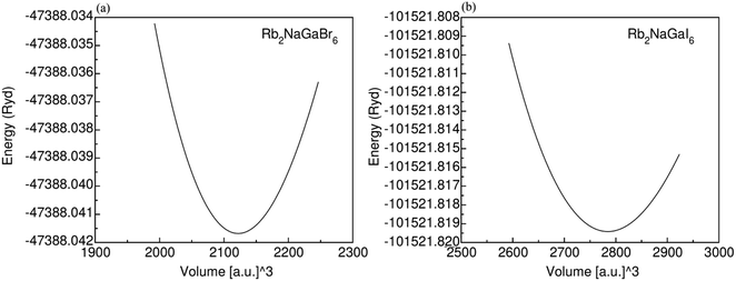
Fig. 1 displays the cubic unit-cell of Rb2NaGaZ6 (Z = Br, I) double perovskites, with space group Fm![[3 with combining macron]](https://www.rsc.org/images/entities/char_0033_0304.gif) m [Fig. 1]. Constituent atoms Rb/Na/Ga/Z are occupied at coordinates (0.25, 0.25, 0.25)/(0.50, 0.50, 0.50)/(0, 0, 0)/(x, 0, 0) and Wyckoff positions at 4b/4a/8c and 24e.33,34 Volume optimization plot between volume and energy of both double perovskites Rb2NaGaBr6 and Rb2NaGaI6 investigated by the Brich–Murnaghan equation of state35 [Fig. 2].
m [Fig. 1]. Constituent atoms Rb/Na/Ga/Z are occupied at coordinates (0.25, 0.25, 0.25)/(0.50, 0.50, 0.50)/(0, 0, 0)/(x, 0, 0) and Wyckoff positions at 4b/4a/8c and 24e.33,34 Volume optimization plot between volume and energy of both double perovskites Rb2NaGaBr6 and Rb2NaGaI6 investigated by the Brich–Murnaghan equation of state35 [Fig. 2].
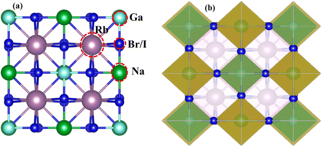 | ||
| Fig. 1 (a) Left side presents a cubic unit-cell ball and (b) the right side image shows polyhedral Rb2NaGaZ6 (Z = Br, I) double-perovskites. | ||
The PBEsol-GGA functional is employed for the analysis of structural parameters. By comparing the ionic radii of iodine (I) and bromine (Br) [Table 2], it is observed that the larger ionic radius of iodine leads to an increase in the lattice constant (ao) from 10.79 Å to 11.81 Å. The calculated values of lattice parameters of Rb2NaGaBr6 are in good agreement with the values reported at materials project database.36 The bulk modulus (Bo) indicates the material's ability to resist volume changes under applied pressure. The lattice constant, as well as Bulk modulus, are linked inversely thus as ao is increasing so the Bo is assumed to decrease. Table 1 show a decrease in values of Bo from 24.3 GPa and 19.46 GPa as I is replaced with Br.
| Parameters | Rb2NaGaBr6 | Rb2NaGaI6 |
|---|---|---|
| PBEsol | PBEsol | |
| ao | 10.79 | 11.81 |
| Bo | 24.34 | 19.46 |
| tG | 0.95 | 0.94 |
| ΔHf | −1.53 | −1.06 |
| C11 | 39.71 | 50.8 |
| C12 | 18.69 | 4.03 |
| C44 | 10.62 | 8.91 |
| B | 25.60 | 19.52 |
| G | 10.57 | 13.20 |
| Y | 27.80 | 32.30 |
| B/G | 2.43 | 1.50 |
| υ | 0.32 | 0.22 |
| A | 1.01 | 0.38 |
To determine the stability of the crystal, Goldsmith tolerance factor tG is computed. For a stable structure, its value must be between 0.81 and 1.11. Our calculated values of the Goldsmith tolerance factors for double perovskites Rb2NaGaI6 and Rb2NaGaBr6 are 0.94 and 0.95, respectively. A reduction in values of enthalpy of formation ΔHf was observed from −1.53 to −1.06 eV as composition is shifted from Br to I.37 The negative sign express the discharge of energy during the construction of these compounds which confirms the stability of the compound. To inspect the mechanical behavior of compounds the elastic constants C11, C22, and C44 are computed.38,39 The Born Criterion condition shows as40
| C11 − C120, C440, C11 + 2C120, BoC11 | (4) |
They assist to find out the estimation of the stiffness of compounds against strains. To examine if the nature of compounds is ductile or brittle the value of the B/G Pugh ratio is measured. The Pugh value of Rb2NaGaBr6 (2.43) is higher than 1.75 and the value of the Poisson ratio (υ) i.e., 0.32 is greater than 0.26 which reveals the ductile nature of this composition. However, when Br is replaced with I, the value of B/G and υ are reduced to 1.50 and 0.22 which uncovers the transformation of composition from ductile to brittle nature.
3.2. Electronic properties
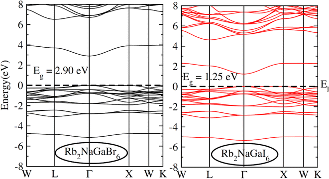
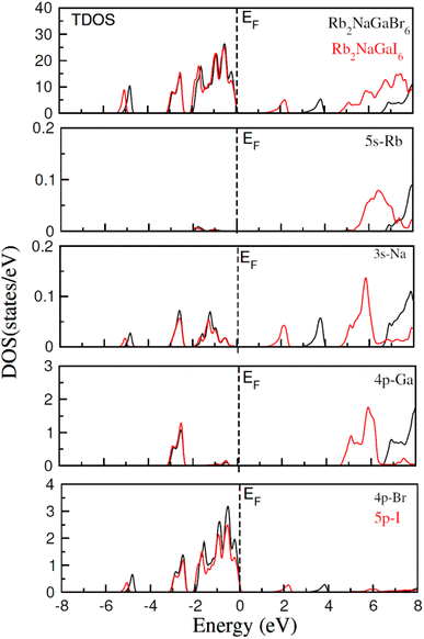
To check the nature of the compound whether it is metallic, insulator or semiconductor we calculated the carrier concentration and their bandgap values. In Fig. 3 band structure of Rb2NaGaZ6 (Z = Br, I) is provided. Investigated band structures inclusive of high symmetry directions are described in 1st Brillouin zones and are computed by mBJ approximation. Fig. 3, depicted the direct bandgap semiconducting nature of compound Rb2NaGaZ6 (Z = Br, I) because the maxima of the valence band (VBM) and minima of the conduction band (CBM) lie at the same Γ point. The value of bandgap for Rb2NaGaBr6 is 2.90 eV and 1.25 eV for Rb2NaGaI6 noted from these band structures. It is clear that the band gap computed for Rb2NaGaBr6 using the TB-mBJ functionals gives larger value compared to the GGA values reported in materials project database where GGA functionals is employed.36 As I has higher ionic radii than Br, which lowered the conduction band edge and thus reduced the bandgap value for Rb2NaGaI6.In addition to this, the calculation of TDOS and PDOS was performed. The graphs depicting the density of states showcase the involvement of various states in the creation of energy bands, as indicated in Fig. 4. The TDOS graph reveals that the energy states in the valence band extend from −5.5 eV to the Fermi level. Furthermore, the conduction band edge is situated at 3.10 eV for Rb2NaGaBr6 and 1.45 eV for Rb2NaGaI6. Examining the PDOS graph closely, it becomes apparent that the valence and conduction band formation heavily relies on the 4p states of Rb and Ga, 3s states of Na, and 4p and 5p states of Br and I. The p-states of halogen atoms predominantly contribute to the valence band maxima, while the 3s-states of Na contribute to the conduction band minima. Interestingly, replacing Br with I causes the states in the conduction band to shift closer to the Fermi level, resulting in a reduced band gap value.
3.3. Optical properties
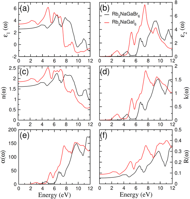
In order to assess the significance of Rb2NaGaZ6 double perovskites (where Z represents Br or I) in the context of solar cell usage, we conducted a thorough analysis of their optical characteristics. The effectiveness of capturing and utilizing incident light in any optoelectronic apparatus relies heavily on interband electronic transitions. A part of incident light induces polarization in material whereas the rest of the light is scattered. To quantify these features the most important parameter is ε(ω) dielectric constant which is utilized to optimize various parameters.| ε = ε1(ω) + îε2(ω) | (5) |
 | (6) |
 | (7) |
| Perovskite | Eg (eV) | ε1(0) | n(0) | R(0) |
|---|---|---|---|---|
| Rb2NaGaBr6 | 3.10 | 2.58 | 1.61 | 0.05 |
| Rb2NaGaI6 | 1.45 | 3.4 | 1.84 | 0.08 |
The understanding of ε1(ω) and ε2(ω) let us to calculate refractive index n(ω), reflectivity R(ω), and absorption coefficient α(ω). These relations can be investigated by utilizing the following equations:
 | (8) |
 | (9) |
Incident energy lower than the bandgap is never able to generate electronic transitions from the valence band (VB) to the conduction band (CB). The value of total reflection varied from Br to I as 0.05 to 0.08 respectively on 0 energy. The refractive index as well as a real part of the dielectric constant are connected by:
| n2 − k2 = ε1(ω) | (10) |
Expand in the values of refractive index n(ω) is witnessed as 1.61 to 1.84 for Rb2NaGaBr6 and Rb2NaGaI6, respectively [see Table 2].
 | (11) |
The coefficient of absorption evaluated the light energy that is absorbed by the semiconductor. The coefficient of extinction k(ω) informs us of the attenuation of light. The light energy attenuation is indicated by α(ω). The light energy that is captivated by the semiconductor is determined by the absorption coefficient α(ω). Additionally, R(ω) evaluated the reflection and scattering of light also Fig. 5. At zero energy. At zero energy R(0) for Rb2NaGaBr6 and Rb2NaGaI6 is 0.05 and 0.08 respectively represented in Table 2. The variation of absorption coefficient α(ω) with energy of the incident photons for Rb2NaGaI6 and Rb2NaGaBr6 are shown in Fig. 5(e). From this plot one can see that when the incident photon's energy is less than that of the band gap of the two materials, electromagnetic radiations are not absorbed. Based on the band gaps of these systems, Fig. 5(e) clearly shows the threshold in absorption for Rb2NaGaI6 is at lower energies compared to Rb2NaGaBr6. Since only for the case of optical band gap a value of α(ω) > 1.0 × 104 cm−1 is realized,41 Fig. 5(e) clearly shows photons absorbed by the studied materials are in accordance with the band gaps of Rb2NaGaI6 and Rb2NaGaBr6, indicating that these two materials are transparent to infrared photons. Compared to the case of hybrid perovskite materials, it can be seen that the optical absorption in the visible region for Rb2NaGaI6 is week.42 However, higher absorption of visible light is seen for Rb2NaGaI6 that can be assigned to the isolated conduction band at lower energies found for this material that causes absorption to begin at lower energies.
3.4. Thermal properties
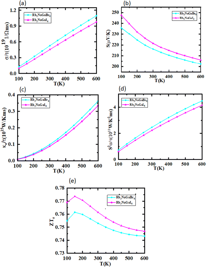
The utilization of certain materials capable of converting waste heat into electrical energy is highly suitable for thermoelectric (TE) devices, making them excellent candidates for energy harvesting. To determine the thermal properties of these double perovskites, calculations were performed using the BoltzTrap code, which is based on transport theory and implemented through WEIN2k. The resulting figures, shown in Fig. 6(a)–(e), illustrate the electrical and thermal conductivities (σ/τ) and (κ/τ), Seebeck coefficient (S), Power Factor (PF), and the figure of merit (ZT) across a temperature range of 200–600 K. A higher Seebeck coefficient indicates the favorable characteristics of a thermoelectric material. In order to achieve a greater ZT value, it is necessary for S, σ, and PF to be higher.A good TE material essentially has bigger values of parameters besides thermal conductivity. The electrical conductivity of each composition approximates the flow of charge. To recognize the sort of material in case it is a conductor, insulator, or semi-conductor, the movement of charges is studied. For an outstanding TE device, the compound should essentially have a high estimation of (σ/τ). The estimation of the electrical conductivity reveals the potential of under-study compositions for designing new TE devices. Thermal conductivity map the flow of heat caused by the temperature gradient across the different ends of the material. This flow of heat could be either caused by electronic transportation called the electronic part of thermal conductivity (κe) or lattice vibration called the lattice part of thermal conductivity (κl). Rb2NaGaBr6 has a higher slope than Rb2NaGaI6 may be because electrons have the most energy. The determined smaller ke/τ and greater σ/τ is in the privilege of TE efficiency. Fermi level takes place at the Eg of the semiconductor also material application can be explained by free charge carrier which bounces from VB to CB. The Seebeck coefficient (S) which illustrates the fraction of potential difference induced due to temperature difference and suggested as thermo-power is indicated in Fig. 6.
 | (12) |
It can be either positive or negative depending on the nature of p-type and n-type.43 As the temperature is increased the S reduces. The figure of merit can be narrated by:
 | (13) |
Generally, the TE performance of any composition is concluded by PF and ZT. The power factor measures the performance of the compound by a collaboration of σ and S. The escalation in PF at higher temperatures is examined as it may cause the existence of a greater number of charge carriers because of the large atomic number.
 | (14) |
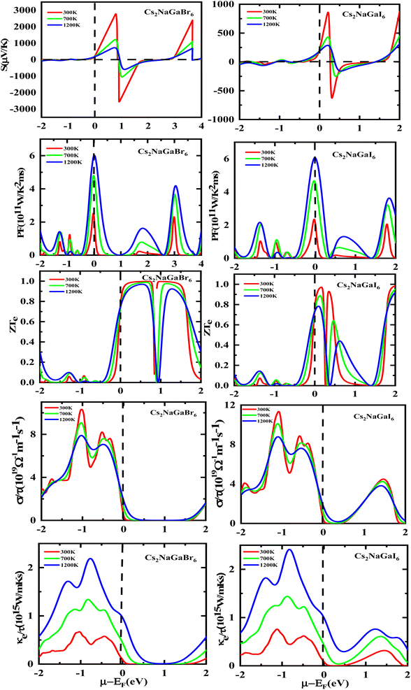
The semiconducting materials with an excess of electrons and holes are termed as n-type and p-type semiconductors, respectively. Although in chemical potential p-type is represented the negative value and n-type materials can be witnessed by a positive value. When we change the temperature, a change is produced in voltage which can be measured by the Seebeck coefficient. Which is written as  . In Fig. 7 we plot the graph of various thermoelectric parameters against chemical potential. The value of S ranges from +2700 μV K−1 to −2700 μV K−1 at 0.8 to 2 (μ − EF) (eV) and 0.3 to 0.4 (μ − EF) (eV) for Rb2NaGaBr6 and Rb2NaGaI6 respectively but as we increase the temperature from 300 K to 700 and 1200 K the curve decreases linearly. Though the negative side of chemical potential gives a minor curve and shows a straight line. The free motion of charge carriers results in the conduction of materials. Fig. 7 shows the values of σ/τ which reveals that as we increase the temperature from 100 K to 600 K the curve of electrical conductivities decreases. At 300 K temperature and −1.0 eV chemical potential, the value of σ/τ was noticed as 10.5 × 10⁻¹⁹ Ω−1 m−1 s−1 and at a maximum temperature of 600 K, the value of σ/τ is noticed on 4.8 × 10⁻¹⁹ Ω−1 m−1 s−1 and n-type is showing a minor contribution at 2 eV for Br. At 300 K Rb2NaGaI6 shows peak at 11.3 × 10⁻¹⁹ Ω−1 m−1 s−1 along with 0.8 eV and n-type doping taking part and demonstrates the curve at 4.2 × 10⁻¹⁹ Ω−1 m−1 s−1 along with 1.5 eV. There is a reverse connection between the Seebeck coefficient and electrical conductivity. The power factor graphs show an increasing trend as we increase the temperature for both compositions. At 300 K we obtain a peak at 2.3 × 10¹¹ W K−2 m−1 s−1 along at 0 eV but as the temperature is increased up to 600 K a maximum curve is obtained at 6 × 10¹¹ W K−2 m−1 s−1 and in p-type doping, the highest peak is obtained at 4.1 × 10¹¹ W K−2 on 3.2 eV for Rb2NaGaBr6. For Rb2NaGaI6 in n-type doping, the maximum is noticed at 2.1 × 10¹¹ W K−2, at 0 eV the power factor has a maximum curve at 6 × 10¹¹ W K−2 and for p-type doping, the PF at 3.8 × 10¹¹ W K−2 is obtained along 1.8 eV. We witnessed by stats that as we increase temperature we can obtain the maximum value of power factor. p-type doping has maximum contributions. Investigated value of the figure of merit investigated at 0.78 eV shows an increase but as we increase the temperature the curve decreases. It was found to be unitary at 300 K at 0.01 eV. The thermal conductivities for n-type and p-type doping is noticed as 0.65 × 10¹⁵ W m−1 K−1 s−1 and 0.80 × 10¹⁵ W m−1 K−1 s−1 at 300 K for Rb2NaGaZ6 (Z = Br, I) respectively.
Fig. 8 shows the carrier concentration plot. As the Seebeck coefficient and carrier concentration are related inversely, as we increase the concentration S decreases. At 250 (μV K−1) the concentration is at −1.7 (e per uc) and as we can see by the graph that by further increasing the value of carrier concentration the value of Seebeck is dropping. In p-type doping we witness a maximum peak for Rb2NaGaI6 at 850 (μV K−1) for 0.1 (e per uc) then it is decreasing linearly. The Power factor will give maximum value at a fixed point after that it will start declining. As PF depends upon S and σ. For Rb2NaGaI6 get maximum peak at 6.1 (μV K−1) for 0.6 (e per uc). The graph for the figure of merit depicts that as we increase the carrier concentration the ZT decreases. For Rb2NaGaBr6 we received a unitary value at 0.01 ZTe and so for Rb2NaGaI6. Electrical and thermal conductivity has a direct relation with carrier concentration. As we start increasing value of Rb2NaGaBr6 for σ/τ from 0 N (e per uc) at 1.8 × 10⁻¹⁹ Ω−1 m−1 s−1 it starts increasing linearly. For Rb2NaGaI6 the curve increases from 0.2 × 10⁻¹⁹ Ω−1 m−1 s−1. For ke/τ as temperature goes on increasing from 300 K to 1200 K the concentration and thermal conductivity also increase. At 1.251015 W m−1 K−1 s−1 along 2 N (e per uc) we get the maximum curve.
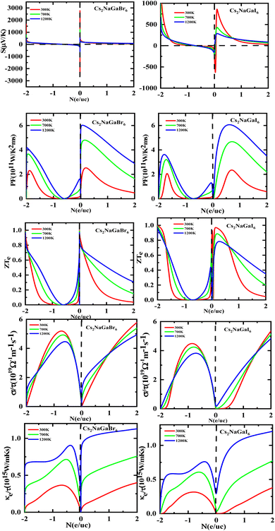 | ||
| Fig. 8 Images of Seebeck (S) coefficients, (PF) power factor, figure (ZT) of merit, electrical as well thermal conductivity graphs versus carrier concentration for DPs Cs2NaGaBr6 and Cs2NaGaI6. | ||
4. Conclusion
In nutshell, we investigated the Rb2NaGaZ6 (Z = Br, I) double perovskites to explore their potential for solar cell application. Opto-electronic and thermoelectric properties were computed by employing first-principles computation using DFT-based WEIN2k software. The structural stability of these compositions was calculated by measuring the value of enthalpy of formation which revealed that Rb2NaGaBr6 was more stable with ΔHf = −1.53. Phase stability was assured by computed values of tolerance factor that was 0.95 and 0.94 for Br and I-based compositions. The analysis of band structure exhibited the direct bandgap nature of both of these compositions and a significant reduction in bandgap value from 2.90 to 1.25 eV upon replacement of Br with I. A low value of reflectivity enlarges the potential of our studied compounds. Electrical and thermal conductivities were greater for Rb2NaGaBr6. While Rb2NaGaI6 has a greater Seebeck coefficient. Better thermal efficiency with high absorption coefficient for UV photons make these compositions the best applicant for energy harvesting devices like solar cells.Data availability
The data included in this paper can be provided on request.Conflicts of interest
There is no conflicts to declare.Acknowledgements
The authors express their gratitude to Princess Nourah Bint Abdulrahman University Researchers Supporting Project (Grant No. PNURSP2024R70), Princess Nourah Bint Abdulrahman University, Riyadh, Saudi Arabia.References
- M. K. Khan, M. I. Khan and M. Rehan, The relationship between energy consumption, economic growth and carbon dioxide emissions in Pakistan, Financ. Innovat., 2020, 6(1), 1–13 CrossRef CAS.
- M. Hussain, M. Rashid, A. Ali, M. F. Bhopal and A. S. Bhatti, Systematic study of optoelectronic and transport properties of cesium lead halide (Cs2PbX6; X= Cl, Br, I) double perovskites for solar cell applications, Ceram. Int., 2020, 46(13), 21378–21387 CrossRef CAS.
- T. Zelai, S. A. Rouf, Q. Mahmood, S. Bouzgarrou, M. A. Amin, A. I. Aljameel and A. Mera, First-principles study of lead-free double perovskites Ga2PdX6 (X= Cl, Br, and I) for solar cells and renewable energy, J. Mater. Res. Technol., 2022, 16, 631–639 CrossRef CAS.
- G. M. Mustafa, A. Slam, S. Saba, N. A. Noor, M. W. Iqbal and A. Dahshan, Optoelectronic and thermoelectric characteristics of halide based double perovskites K2YAgX6 (X= Br, I) for energy storage applications, Polyhedron, 2023, 229, 116184 CrossRef CAS.
- M. A. Razzaq and T. Islam, Optoelectronic study of double perovskite Rb2SnBr6: a first principles calculations, Global J. Mater. Sci. Eng., 2020, 2, 1–5 Search PubMed.
- J. J. Yoo, G. Seo, M. R. Chua, T. G. Park, Y. Lu, F. Rotermund and J. Seo, Efficient perovskite solar cells via improved carrier management, Nature, 2021, 590(7847), 587–593 CrossRef CAS PubMed.
- M. W. Mukhtar, M. Ramzan, M. Rashid, A. Hussain, G. Naz, Y. O. Ciftci and S. Znaidia, Systematic study of optoelectronic and thermoelectric properties of new lead-free halide double perovskites A2KGaI6 (A= Cs, Rb) for solar cell applications via ab-initio calculations, Mater. Sci. Eng., B, 2022, 285, 115957 CrossRef.
- Y. Zheng, R. Su, Z. Xu, D. Luo, H. Dong, B. Jiao and R. Zhu, Perovskite solar cell towards lower toxicity: a theoretical study of physical lead reduction strategy, Sci. Bull., 2019, 64(17), 1255–1261 CrossRef CAS PubMed.
- C. Zhang, L. Gao, S. Teo, Z. Guo, Z. Xu, S. Zhao and T. Ma, Design of a novel and highly stable lead-free Cs 2 NaBiI 6 double perovskite for photovoltaic application, Sustainable Energy Fuels, 2018, 2(11), 2419–2428 RSC.
- M. A. Amin, G. Nazir, Q. Mahmood, J. Alzahrani, N. A. Kattan, A. Mera and T. Altalhi, Study of double perovskites X2InSbO6 (X= Sr, Ba) for renewable energy; alternative of organic-inorganic perovskites, J. Mater. Res. Technol., 2022, 18, 4403–4412 CrossRef CAS.
- Q. Mahmood, T. Zelai, M. Hassan, G. Nazir, H. Albalawi, N. Sfina and M. A. Amin, Study of lead-free double perovskites X2AgBiI6 (X= K, Rb, Cs) for solar cells and thermoelectric applications, J. Mater. Res. Technol., 2023, 22, 913–922 CrossRef CAS.
- P. A. Owusu and S. Asumadu-Sarkodie, A review of renewable energy sources, sustainability issues and climate change mitigation, Cogent Eng., 2016, 3(1), 1167990 CrossRef.
- T. I. Al-Muhimeed, A. Shafique, A. A. AlObaid, M. Morsi, G. Nazir, M. M. AL-Anazy and Q. Mahmood, New lead-free double perovskites X2GeI6 (X= K, Rb, Cs) for solar cells, and renewable energy as an alternate of hybrid perovskites, Int. J. Energy Res., 2021, 45(13), 19645–19652 CrossRef CAS.
- Q. Mahmood, M. Younas, M. G. B. Ashiq, S. M. Ramay, A. Mahmood and H. M. Ghaithan, First principle study of lead-free double perovskites halides Rb2Pd (cl/Br) 6 for solar cells and renewable energy devices: a quantum DFT, Int. J. Energy Res., 2021, 45(10), 14995–15004 CrossRef CAS.
- A. Wang, C. Zuo, X. Niu, L. Ding, J. Ding and F. Hao, Recent promise of lead-free halide perovskites in optoelectronic applications, Chem. Eng. J., 2022, 138926 Search PubMed.
- S. Ghosh and B. Pradhan, Lead-Free Metal Halide Perovskite Nanocrystals: Challenges, Applications, and Future Aspects, ChemNanoMat, 2019, 5(3), 300–312 CrossRef CAS.
- S. Khalfin and Y. Bekenstein, Advances in lead-free double perovskite nanocrystals, engineering band-gaps and enhancing stability through composition tunability, Nanoscale, 2019, 11(18), 8665–8679 RSC.
- M. Ghasemi, M. Hao, M. Xiao, P. Chen, D. He, Y. Zhang and X. Wen, Lead-free metal-halide double perovskites: from optoelectronic properties to applications, Nanophotonics, 2020, 10(8), 2181–2219 CrossRef.
- L. Chu, W. Ahmad, W. Liu, J. Yang, R. Zhang, Y. Sun and X. A. Li, Lead-free halide double perovskite materials: a new superstar toward green and stable optoelectronic applications, Nano-Micro Lett., 2019, 11(1), 1–18 Search PubMed.
- M. Faizan, G. Murtaza, S. H. Khan, A. Khan, A. Mehmood, R. Khenata and S. Hussain, First-principles study of the double perovskites Sr2XOsO6 (X= Li, Na, Ca) for spintronics applications, Bull. Mater. Sci., 2016, 39(6), 1419–1425 CrossRef CAS.
- D. Behera and S. K. Mukherjee, Optoelectronics and transport phenomena in Rb2InBiX6 (X= Cl, Br) compounds for renewable energy applications: a DFT insight, Chemistry, 2022, 4(3), 1044–1059 CrossRef CAS.
- A. M. Mebed, S. Al-Qaisi and M. A. Ali, Study of optoelectronic and thermoelectric properties of double perovskites Rb2AgBiX6 (X= Br, I): by DFT approach, Eur. Phys. J. Plus, 2022, 137(8), 1–8 Search PubMed.
- Q. Mahmood, M. H. Alhossainy, M. S. Rashid, T. H. Flemban, H. Althib, T. Alshahrani and A. Laref, First-principles study of lead-free double perovskites Rb2TeX6 (X= Cl, Br, and I) for solar cells and renewable energy, Mater. Sci. Eng., B, 2021, 266, 115064 CrossRef CAS.
- M. Manzoor, D. Bahera, R. Sharma, F. Tufail, M. W. Iqbal and S. K. Mukherjee, Investigated the structural, optoelectronic, mechanical, and thermoelectric properties of Sr2BTaO6 (B= Sb, Bi) for solar cell applications, Int. J. Energy Res., 2022, 46(15), 23698–23714 CrossRef CAS.
- Q. Mahmood, T. Zelai, M. Hassan, G. Nazir, H. Albalawi, N. Sfina and M. A. Amin, Study of lead-free double perovskites X2AgBiI6 (X= K, Rb, Cs) for solar cells and thermoelectric applications, J. Mater. Res. Technol., 2023, 22, 913–922 CrossRef CAS.
- A. Aziz, S. A. Aldaghfag, M. Zahid, J. Iqbal, M. Yaseen and H. H. Somaily, Theoretical investigation of X2NaIO6 (X= Pb, Sr) double perovskites for thermoelectric and optoelectronic applications, Phys. B, 2022, 630, 413694 CrossRef CAS.
- J. Yang, Y. Zhou, Y. Dedkov and E. Voloshina, Dirac Fermions in Half-Metallic Ferromagnetic Mixed Cr 1− x MxPSe3 Monolayers, Adv. Theory Simul., 2020, 3(12), 2000228 CrossRef CAS.
- K. Choudhary, Q. Zhang, A. C. Reid, S. Chowdhury, N. Van Nguyen, Z. Trautt and F. Tavazza, Computational screening of high-performance optoelectronic materials using OptB88vdW and TB-mBJ formalisms, Sci. Data, 2018, 5(1), 1–12 CrossRef PubMed.
- F. Di Giacomo, A. Fakharuddin, R. Jose and T. M. Brown, Progress, challenges and perspectives in flexible perovskite solar cells, Energy Environ. Sci., 2016, 9(10), 3007–3035 RSC.
- W. Khan, S. Azam, M. B. Kanoun and S. Goumri-Said, Optoelectronic structure and related transport properties of BiCuSeO-based oxychalcogenides: first principle calculations, Solid State Sci., 2016, 58, 86–93 CrossRef CAS.
- W. Khan, S. Azam, M. B. Kanoun and S. Goumri-Said, Optoelectronic structure and related transport properties of BiCuSeO-based oxychalcogenides: first principle calculations, Solid State Sci., 2016, 58, 86–93 CrossRef CAS.
- G. A. Mersal, H. Alkhaldi, G. M. Mustafa, Q. Mahmood, A. Mera, S. Bouzgarrou and M. A. Amin, Study of half metallic ferromagnetism and thermoelectric properties of spinel chalcogenides BaCr2X4 (X= S, Se, Te) for spintronic and energy harvesting, J. Mater. Res. Technol., 2022, 18, 2831–2841 CrossRef CAS.
- E. Haque and M. A. Hossain, Electronic, phonon transport and thermoelectric properties of Cs2InAgCl6 from first-principles study, Comput. Condens. Matter, 2019, 19, e00374 CrossRef.
- H. Albalawi, G. M. Mustafa, S. Saba, N. A. Kattan, Q. Mahmood, H. H. Somaily and M. A. Amin, Study of optical and thermoelectric properties of double perovskites Cs2KTlX6 (X= Cl, Br, I) for solar cell and energy harvesting, Mater. Today Commun., 2022, 32, 104083 CrossRef CAS.
- F. Birch, Finite elastic strain of cubic crystals, Phys. Rev., 1947, 71(11), 809 CrossRef CAS.
- A. Jain, S. P. Ong, G. Hautier, W. Chen, W. D. Richards, S. Dacek, S. Cholia, D. Gunter, D. Skinner, G. Ceder and K. A. Persson, APL Mater., 2013, 1, 011002 CrossRef.
- Q. Mahmood, T. Ghrib, A. Rached, A. Laref and M. A. Kamran, Probing of mechanical, optical and thermoelectric characteristics of double perovskites Cs2GeCl/Br6 by DFT method, Mater. Sci. Semicond. Process., 2020, 112, 105009 CrossRef CAS.
- N. A. Noor, Q. Mahmood, M. Rashid, B. U. Haq, A. Laref and S. A. Ahmad, Ab-initio study of thermodynamic stability, thermoelectric and optical properties of perovskites ATiO3 (A= Pb, Sn), J. Solid State Chem., 2018, 263, 115–122 CrossRef CAS.
- N. A. Noor, M. Hassan, M. Rashid, S. M. Alay-e-Abbas and A. Laref, Systematic study of elastic, electronic, optical and thermoelectric properties of cubic BiBO3 and BiAlO3 compounds at different pressure by using ab-initio calculations, Mater. Res. Bull., 2018, 97, 436–443 CrossRef CAS.
- F. Mouhat and F. X. Coudert, Necessary and sufficient elastic stability conditions in various crystal systems, Phys. Rev. B: Condens. Matter Mater. Phys., 2014, 90(22), 224104 CrossRef.
- M. A. Green and M. J. Keevers, Optical properties of intrinsic silicon at 300 K, Prog. Photovoltaics, 1995, 3, 189–192 CAS.
- M. Kato, T. Fujiseki, T. Miyadera, T. Sugita, S. Fujimoto, M. Tamakoshi, M. Chikamatsu and H. Fujiwara, Universal rules for visible-light absorption in hybrid perovskite materials, J. Appl. Phys., 2017, 121, 115501 CrossRef.
- N. A. Noor, M. B. Saddique, B. U. Haq, A. Laref and M. Rashid, Investigations of half-metallic ferromagnetism and thermoelectric properties of cubic XCrO3 (X= Ca, Sr, Ba) compounds via first-principles approaches, Phys. Lett. A, 2018, 382(42–43), 3095–3102 CrossRef CAS.
| This journal is © The Royal Society of Chemistry 2023 |

