 Open Access Article
Two-dimensional β-noble-transition-metal chalcogenide: novel highly stable semiconductors with manifold outstanding optoelectronic properties and strong in-plane anisotropy
Qing-Yuan Chen *a,
Fei-Jie Huanga,
Ju-Qi Ruana,
Yi-Fen Zhaoa,
Fen Lia,
Hai Yang*a,
Yao He
 b and
Kai Xiongc
aSchool of Physical Science and Technology, Kunming University, Kunming 650214, China. E-mail: qingyuanchen212@163.com; kmyangh@263.net
bDepartment of Physics, Yunnan University, No.2 Green Lake North Road, Wu Hua Qu, Kunming 650091, Yunnan Province, China
cMaterials Genome Institute, School of Materials and Energy, Yunnan University, Kunming 650091, China
First published on 2nd October 2023
Abstract
In this work, five two-dimensional (2D) noble-transition-metal chalcogenide (NTMC) semiconductors, namely β-NX (N = Au, Ag; X = S, Se, Te), were designed and predicted by first-principles simulations. Structurally, the monolayer β-NX materials have good energetic, mechanical, dynamical, and thermal stability. They contain two inequivalent noble-transition-metal atoms in the unit cell, and the N–X bond comprises a partial ionic bond and a partial covalent bond. Regarding the electronic properties, the β-NX materials are indirect-band-gap semiconductors with appropriate band-gap values. They have tiny electron effective masses. The hole effective masses exhibit significant differences in different directions, indicating strongly anisotropic hole mobility. In addition, the coexistence of linear and square-planar channels means that the diffusion and transport of carriers should be anisotropic. In terms of optical properties, the β-NX materials show high absorption coefficients. The absorption and reflection characteristics reveal strong anisotropy in different directions. Therefore, the β-NX materials are indirect-band-gap semiconductors with good stability, high absorption coefficients, and strong mechanical, electronic, transport, and optical anisotropy. In the future, they could have great potential as 2D semiconductors in nano-electronics and nano-optoelectronics.
1 Introduction
Two-dimensional (2D) transition-metal dichalcogenides (TMDs) are a class of materials characterized by an abundance of possible constituent elements, good stability, an indirect–direct band-gap transition when decreasing the number of layers, a suitable band-gap value, comprehensive optical response, strong Coulomb interactions, and strong light–matter coupling. Such exceptional properties have made 2D TMDs the subject of considerable attention from researchers in new energy technology and nano-optoelectronics. Nonetheless, research results suggest that the low carrier mobility (about 200–500 cm2 V−1 s−1) of 2D TMDs limits their large-scale application in related fields.1–7 Consequently, researchers aim to design and develop a new 2D semiconductor material with superior properties to traditional TMDs, but with higher carrier mobility, thereby striving to facilitate the application of 2D materials in new energy technology and nano-optoelectronics, stimulating the development of these domains.In recent years, noble-transition-metal dichalcogenides (NTMDs), composed of noble-transition-metal and chalcogenide elements such as PtTe2, PdTe2, PtSe2, PtS2, PdS2, and PdSe2, have been given much attention.8–23 Studies have discovered that these materials boast distinct structures and varieties of phases, adjustable band gaps across a broad range, high carrier mobility, strong anisotropy, and outstanding stability in air and at high temperatures. Moreover, in contrast to most classical TMDs, the d orbitals of NTMDs are almost filled, and the pz orbitals of interlayer sulfur atoms are highly hybridized, driving a strong interlayer influence and interactions. Due to all these superior features, NTMDs are seen as being highly viable for usage in electronics, optoelectronics, renewable energy, catalysis, and sensors.8–23
Recently, inspired by the excellent characteristics of 2D NTMD materials, researchers have found a new type of layered structure, namely noble-transition-metal chalcogenide (NTMC) materials. Monolayer β-AuSe was predicted as a new 2D material with good stability, appropriate band gap, high visible-light absorption, and ultra-high carrier mobility (103–105 cm2 V−1 s−1) by the first-principles calculations of Gong et al. in 2019.24 Its exfoliation energy is close to those of graphene and phosphorene. Moreover, it can be prepared by liquid exfoliation or mechanical exfoliation. Besides, its electronic and optical properties exhibit strong in-plane anisotropy.24 In the same year, Machogo et al. synthesized 2D β-AuSe via the colloid method using a gold chloride precursor and comprehensively studied its structural properties.25 Later, Bai et al. used the density functional theory (DFT) method to study 2D β-AuSe. They found that monolayer β-AuSe has excellent dynamic and thermodynamic stability. Its formation energy can reach −7.87 eV per atom and responds well to UV light.26 In 2020, Tang et al. adopted the DFT method to calculate the ultra-high and anisotropic carrier mobility of monolayer β-AuSe. Furthermore, they investigated the contribution of two non-equivalent Au channels to its electronic properties.27 In 2021, Yin et al. used the first-principles method to design a Z-type AuSe/SnS heterojunction photocatalytic hydrogen-evolving material. They found that this material can respond to most visible and UV light, and its photocatalytic hydrogen evolution efficiency can reach 23.96%.28 In 2022, Xie et al. found that single-layer XSe (X = Cu, Ag, Au) has excellent electric transport properties (ultra-high Seebeck coefficient and carrier mobility), and all of the XSe materials exhibit high anisotropy and low thermal conductivity.29 It can be seen that the 2D β-NTMC, a new 2D material that can be prepared experimentally, has suitable formation energy and exfoliation energy, good stability, appropriate band-gap values, high carrier mobility, strong anisotropy, and other excellent optoelectronic properties. It has good application prospects in the fields of new energy technology and optoelectronics.
Inspired by these studies, we aim to design and construct a new 2D material with good stability, appropriate band gap, and fascinating optical properties based on the novel 2D β-AuSe. We hope to extend the family members of the new 2D β-NTMC materials and further promote their application as high-performance 2D materials in nano-electronics and nano-optics.
This work employs first-principles calculations to predict five 2D NTMC semiconductors, monolayer β-NX (N = Au, Ag; X = S, Se, Te). In terms of structural properties, they have reasonable cohesive energy and good mechanical, dynamical, and thermal stability. The N–X bond is composed of partial ionic and covalent bonds. Meanwhile, there are lone pairs of electrons around the X atom. In terms of electronic properties, the indirect band-gap values of monolayer AgS, AgSe, AgTe, AuS, and AgTe are 1.55, 1.25, 0.91, 2.13, and 1.36 eV, respectively, using the Heyd–Scuseria–Ernzerhof (HSE06) screened hybrid functional method. They have tiny electron effective masses. The effective hole masses show significant differences in different directions, indicating strongly anisotropic hole mobility. The linear N(2) and square-planar N(4) channels give the carriers strong anisotropic diffusion and transport. The β-NX materials show strong anisotropy in different directions regarding the optical properties. Along the x-direction, the central absorption and reflection regions are in the ultraviolet region, far higher in wavelength than the visible-light and infrared region, and they have good transparency in the visible-light and infrared region. Along the y-direction, the absorption ability in the visible light region is enhanced, and the primary reflection ability is in the visible-light region, with good transparency in the infrared region. The β-NX materials are indirect-band-gap semiconductors with good stability, high absorption coefficients, and strong mechanical, electronic, transport, and optical anisotropy, making them promising for field-effect transistors (FETs), solar cells, polarizers, LEDs, catalysis, sensors, and other nano-electronics and nano-optoelectronics.
2 Computational method
The Vienna Ab initio Simulation Package (VASP) developed at the University of Vienna was employed for all calculations performed in this work.30,31 We employed the projector-augmented wave approximation method to manage the electron interactions, setting the plane-wave energy cutoff to 600 eV.31,32 Perdew, Burke, and Ernzerhof's generalized gradient approximation (GGA-PBE) method was chosen to deal with the exchange–correlation energy.30,33 The HSE06 hybrid functional method was used to calculate the electronic and optical properties for greater precision.34,35 Additionally, given the abundance of d electrons in β-NX, we conducted comparative calculations with and without spin–orbit coupling (SOC) in the band-structure analyses. We used gamma-central K-points with a grid size of 16 × 27 × 1 in the Brillouin zone, with an energy convergence criterion of 10−7 eV and a convergence tolerance of forces of 0.01 eV Å−1. In order to eliminate the interaction between different layers, we added a vacuum of 30 Å in the z-direction to the monolayer β-NX structure model.3 Results
3.1 Structural properties
Determining the structural parameters of new materials is the most critical point in studying them. After sufficient structural optimization, we obtained the structural parameters of all the β-NX materials (N = Au, Ag; X = S, Se, Te). Panels (a–d) in Fig. 1 are schematic diagrams of the monolayer β-NX structure from different views, and Fig. 1(e) is its Brillouin zone. The structures of β-NX (N = Au, Ag; X = S, Se, Te) are highly similar to that of β-AuSe, with a sandwich-like structure. The structures have two types of inequivalent noble-transition-metal atoms: the N(4) atoms connected to four X atoms and the N(2) atoms connected to two X atoms. In addition, the unit cell of β-NX consists of two N atoms and two X atoms. The space groups are all P2/m. The specific lattice parameters of β-NX (N = Au, Ag; X = S, Se, Te) are listed in Table 1.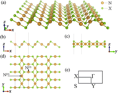 | ||
| Fig. 1 (a–d) Schematic diagrams of the monolayer β-NX structure from different views. Panel (e) is the Brillouin zone of monolayer β-NX. | ||
| Material | a (Å) | b (Å) | α (deg) | β (deg) | γ (deg) | Cohesive energy (eV per atom) | Band-gap (eV) | |||
|---|---|---|---|---|---|---|---|---|---|---|
| PBE | PBE + SOC | HSE06 | ||||||||
| AgS | 6.054 | 3.570 | 90.000 | 91.083 | 90.000 | 2.70 | 0.98 | 0.96 | 1.55 | This work |
| AgSe | 6.039 | 3.755 | 90.000 | 92.400 | 90.000 | 2.53 | 0.87 | 0.74 | 1.25 | This work |
| AgTe | 6.247 | 4.087 | 90.000 | 93.685 | 90.000 | 2.42 | 0.66 | 0.49 | 0.91 | This work |
| AuS | 6.254 | 3.541 | 90.000 | 88.986 | 90.000 | 3.13 | 1.35 | 1.28 | 2.13 | This work |
| AuSe | 6.262 | 3.663 | 90.000 | 90.000 | 90.000 | — | — | — | 1.66 | Ref. 24 |
| AuTe | 6.667 | 4.010 | 90.000 | 90.513 | 90.000 | 2.83 | 0.97 | 0.66 | 1.36 | This work |
To examine the β-NX monolayer's energetic stability, we calculated its cohesive energy. The equation for cohesive energy calculation is as follows:
 | (1) |
The dynamical stability is studied using the calculated phonon dispersion curves (Fig. 2) and atom-projected phonon density-of-states (PhDOS) (Fig. 3). From Fig. 2, we find no imaginary frequencies over the entire Brillouin zones, which indicates that the β-NX structures are dynamically stable. We further analyze the dynamical properties of β-NX based on the PhDOS (Fig. 3). We observe that the phonon frequencies of β-NX are mainly concentrated in three ranges. For example, for β-AgS, the phonon frequencies are mainly concentrated in the low-frequency range (0–4.18 THz), the mid-frequency range (6.72–8.39 THz), and the high-frequency range (9.10–9.94 THz). Two phonon gaps are also observed. Notably, within the mid-frequency range in the dispersion spectrum of β-AuS, there is an overlap of dispersion curves, resulting in only one phonon gap in the dispersion spectrum of β-AuS. In addition, for β-AgTe, there is a relatively dispersionless acoustic branch in the range of 1.79–2.23 THz, which is mainly contributed by the vibration of Ag atoms. We interpret that this dispersionless branch is mainly caused by the much more significant contribution of Ag atoms to the vibration than Te atoms. The highest phonon frequencies for β-AgS, AgSe, AgTe, AuS, and AuTe are 9.94, 7.23, 6.00, 10.60, and 5.60 THz (corresponding to 331.53 cm−1, 241.34 cm−1, 200.14 cm−1, 353.75 cm−1, and 186.84 cm−1, respectively). The highest phonon frequency is contributed by both N and X atoms, indicating the presence of strong N–X bonds in β-NX. In the mid-frequency range, the vibration contribution is mainly from the X atom, while in the low-frequency range, it is contributed by both N and X atoms. We also found that the phonon frequencies and phonon gaps of β-NX vary with different compositions of elements. Specifically, when the N atoms change from Ag to Au, the highest phonon frequency increases, while the phonon gap in the higher frequency range decreases. On the other hand, when the X atoms change from S to Se and then to Te, the maximum phonon frequencies in all three frequency ranges decrease, and the phonon gap in the higher frequency range increases, while the phonon gap in the lower frequency range decreases. Therefore, the phonon gap of β-NX can be controlled through atom and alloy engineering.
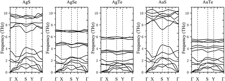 | ||
| Fig. 2 The phonon dispersion spectra corresponding to the monolayer β-AgS, AgSe, AgTe, AuS, and AuTe, from left to right. | ||
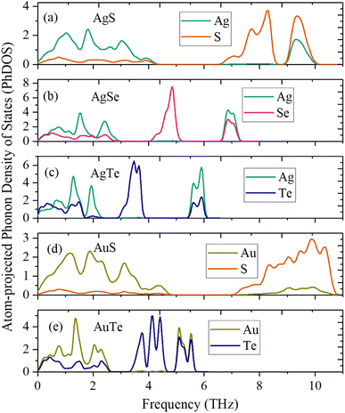 | ||
| Fig. 3 Atom-projected phonon density of states (PhDOS) of the monolayer β-AgS (a), AgSe (b), AgTe (c), AuS (d), and AuTe (e). | ||
We subsequently investigated the mechanical stability of β-NX according to the Born–Huang elastic stability criterion. This criterion comprises three aspects: (i) C11 > 0, (ii) C66 > 0, and (iii) C11C22 > C12C12.38 Here, Cij represents the second-order in-plane elastic constant calculated using the energy-strain method. The calculation process is performed using the following equation: Cij = (1/S0)(∂2E/∂εi∂εj). In this equation, E represents the strain energy, and εij denotes the corresponding in-plane strains ranging from −1.5% to 1.5%, with an interval of 0.5%. S represents the equilibrium area of the system.38 The calculation results are presented in Table 2, and indicate that all the β-NX samples exhibit good mechanical stability.38–43 To further investigate the mechanical properties of β-NX, we calculated the orientation-dependent Young's modulus and Poisson's ratio (Fig. 4 and Table 2). The calculation process involves the following formulas:
 | (2) |
 | (3) |
| Material | C11 | C22 | C12 | C66 | Y2Dmax(θ) | Y2Dmin(θ) | νmax(θ) | νmin(θ) |
|---|---|---|---|---|---|---|---|---|
| AgS | 7.256 | 27.462 | 2.148 | 2.398 | 26.826 | 6.419 | 0.498 | 0.078 |
| AgSe | 4.605 | 22.810 | 0.934 | 1.270 | 22.621 | 3.659 | 0.569 | 0.041 |
| AgTe | 2.675 | 21.420 | −0.119 | 0.457 | 21.414 | 1.497 | 0.717 | −0.044 |
| AuS | 13.065 | 41.409 | 4.058 | 5.380 | 40.149 | 12.574 | 0.397 | 0.098 |
| AuTe | 6.527 | 32.428 | 1.700 | 2.064 | 31.985 | 5.638 | 0.530 | 0.052 |
 | ||
| Fig. 4 The orientation-dependent (a) Young's moduli (Y2D(θ)) and (b) Poisson's ratios (ν(θ)) for monolayer β-NX. | ||
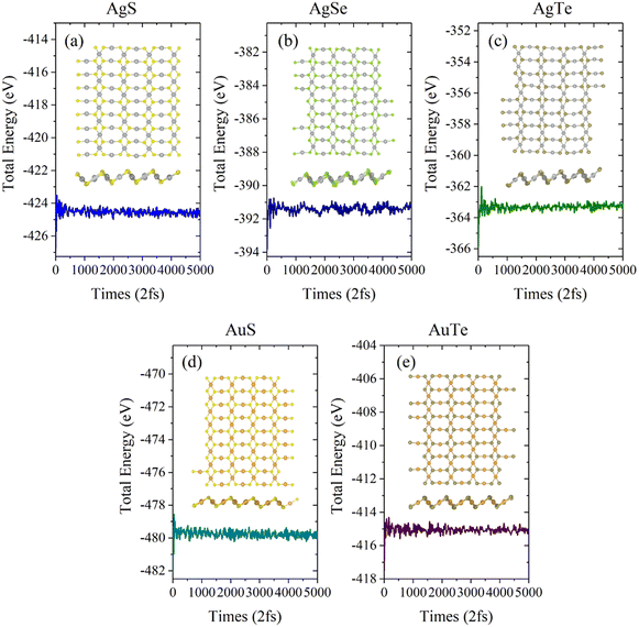
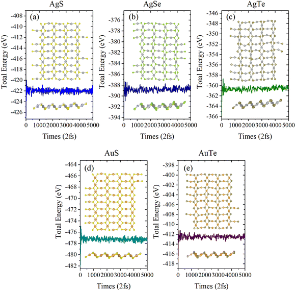
Next, we investigated the thermal stability of β-NX monolayers via ab initio molecular dynamics (AIMD) calculations (Fig. 5 and 6). We found that, after 10 ps of AIMD simulation at 300 K and 600 K, the structures can still maintain good stability. This indicates that the β-NX monolayers show good stability at temperatures up to 300 K and 600 K, verifying their thermal stability.
In short, the β-NX monolayers have energetic, dynamical, mechanical, and thermal stability, which implies that they can be feasibly synthesized in future experiments.
3.2 Electronic properties
In order to study the application prospects of 2D β-NX materials in the field of nano-optoelectronics, we comprehensively calculated their electronic properties. Due to the abundance of d electrons in β-NX, we first tested the band structure (Fig. 7) calculated with/without spin–orbit coupling (SOC). This reveals that as the chalcogen element changes from S to Te, the difference between the cases with and without SOC in the band structure becomes increasingly apparent. However, in general, similar to the previous study on the band structure of β-AuSe, the main change in the band structure near the Fermi level when considering SOC is a slight decrease in the band gap. Considering the large number of calculations in this paper and the slight influence of the SOC effect on the results, in the following sections, we will mainly discuss the results obtained using the method without the SOC effect.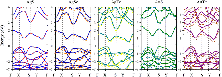 | ||
| Fig. 7 Band structures of the monolayer β-AgS, AgSe, AgTe, AuS, and AuTe from left to right. PBE calculations without the SOC effect are the solid lines, and PBE + SOC effect are the dotted lines. | ||
To make the calculated results more consistent with experimental values, we adopted the HSE06 hybrid functional method to calculate the band structures and electronic density of states (DOS) (Fig. 8). The Fermi level is set to zero. All five β-NX materials are indirect-band-gap semiconductors. The valence band maximum (VBM) is at the high symmetry X point, and the conduction band minimum (CBM) is at the A point, between the high symmetry Y and Γ points. The band gaps of AgS, AgSe, AgTe, AuS, and AgTe are 1.55, 1.25, 0.91, 2.13, and 1.36 eV, respectively, when using the HSE06 method. Combined with previous studies, the indirect band gap of β-AuSe is 1.79 eV. Thus, all the β-NX (N = Au, Ag; X = S, Se, Te) materials are semiconductors with suitable band gaps and have good potential in the nano-semiconductor and nano-optoelectronic materials field. Furthermore, when the noble-transition-metal element N is the same, the band gap of β-NX decreases as the chalcogen element changes from S to Te, indicating that the energy of the band containing the VBM located at the S and Y points gradually decreases, and the energy gap between the CBM band and the higher-energy conduction band gradually decreases. Additionally, when the chalcogen element X is the same, the band gap of AuX is more significant than that of AgX. To achieve a more comprehensive analysis, we calculated the partial electronic density of states (Fig. 9). Fig. 9 shows that the VBMs of β-NX are mainly composed of X-p and N-d electrons, as well as some N-s electrons, while the CBM is mainly composed of X-p and N-d electrons. Besides, as the X atom changes from S to Te, the proportion of N-d electrons at the VBM decreases, and the proportion of X-p electrons increases.
 | ||
| Fig. 8 The band structures and total density of states (DOS) of β-AgS (a), AgSe (b), AgTe (c), AuS (d), and AuTe (e) when using the HSE06 method. | ||
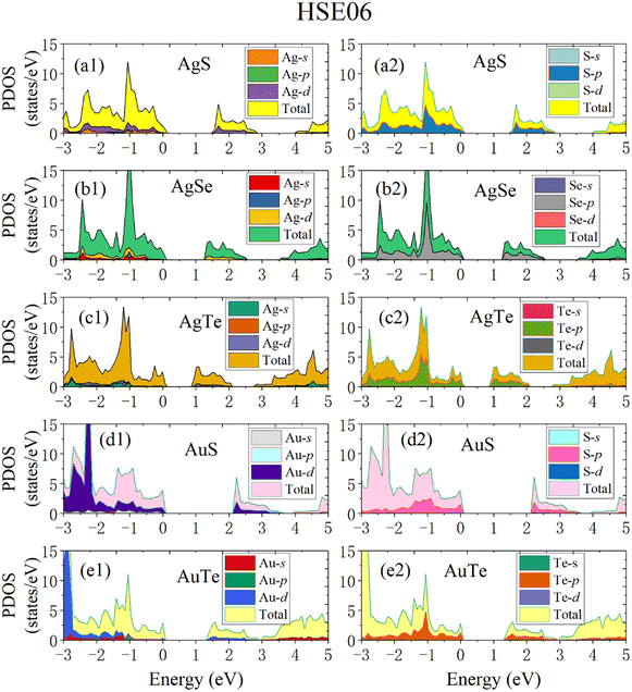 | ||
| Fig. 9 The calculated partial density of states (PDOS) of β-AgS (a1 and a2), AgSe (b1 and b2), AgTe (c1 and c2), AuS (d1 and d2) and AuTe (e1 and e2) when using the HSE06 method. | ||
Furthermore, we calculated the electron localization functions (ELFs) according to the following equation:
 | (4) |
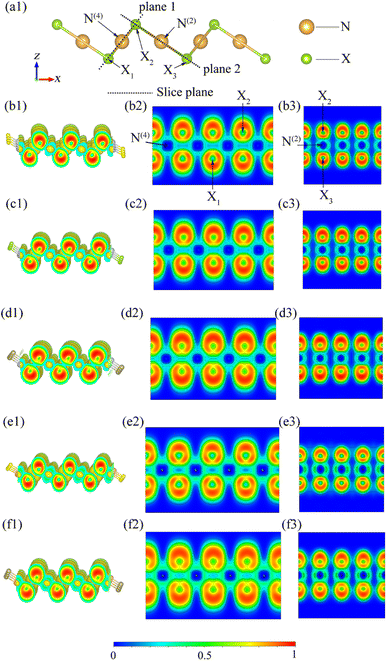
To ensure the systematic analysis of the ELFs and gain a deep understanding of the electronic properties of inequivalent atoms, we plotted 3D and 2D ELF figures containing inequivalent N atoms on two planes (Fig. 10). Here, the range of ELF values is selected to be from 0 to 1. ELF = 0, 0.5, and 1 indicates that the electron is in the complete nonlocality, electron-gas, and perfect localization states, respectively. Fig. 10 shows that, firstly, the ELF values near the X atom are close to 1 for all the β-NX monolayers, which means that the electrons are mainly localized around the X atom, and the ELF values are zero around both N(4) and N(2), indicating that there should be an ionic bond between the N atom and the X atom. Secondly, based on previous studies, the ELF values near the central position within the bonds are beyond 0.75, demonstrating that the chemical bonding is covalent. Thirdly, there is significant electron aggregation near the X atom pointing away from the N(4)–X and N(2)–X bonds, which indicates the presence of lone-pair electrons (LPEs) on the X atom. That is to say, in β-NX, both the N(4)–X and N(2)–X bonds are composed of partial ionic bonds and partial covalent bonds, and there are lone-pair electrons around the X atoms.45,48–50 Such LPEs are more inclined to be between layers, which gives β-NX excellent conductivity. Additionally, the linear N(2) channel is intermittent along the y-direction and continuous along the x-direction, whereas the square-planar N(4) channel is the opposite. Moreover, electron-gas characteristics, which correspond to the green regions in Fig. 10, give monolayer β-NX a flexible quality.48
Additionally, we calculated the effective masses of holes and electrons of the VBM and CBM along different directions for the different β-NX materials. The equation used in the calculation is shown in eqn (3), where ħ is the reduced Planck constant, and k and E represent the wave vector and corresponding energy, respectively.
 | (5) |
The results are shown in Table 3. We found that near the CBM, the effective masses of electrons for all the β-NX materials are small, and the effective masses of electrons along the A–Y and A–Γ directions are almost the same. Near the VBM, the effective masses of holes for all the β-NX materials along the X–S direction are much larger than those along the X–Γ direction, showing a strong anisotropy.24,27 Thus, based on our above research on the electronic properties of β-NX, we believe that β-NX should have promising prospects in the field of nanoelectronics applications.
| Material | Carrier type | m*(me) | Carrier type | m*(me) | ||
|---|---|---|---|---|---|---|
| A–Y | A–Γ | X–S | X–Γ | |||
| AgS | Electrons | 0.33 | 0.32 | Holes | −3.44 | −1.09 |
| AgSe | 0.28 | 0.25 | −2.63 | −1.38 | ||
| AgTe | 0.25 | 0.21 | −5.34 | −1.48 | ||
| AuS | 0.43 | 0.38 | −9.95 | −0.60 | ||
| AuTe | 0.26 | 0.23 | −4.99 | −0.67 | ||
3.3 Optical properties
Next, we will discuss the optical properties of β-NX. We first calculated the imaginary part of the dielectric function using eqn (6) and obtained the real part of the dielectric function through the Kramers–Kronig relation (eqn (7)).51 η is an infinitesimal number.51 The relation between the complex dielectric function and the absorption and reflection coefficients (eqn (8)–(10)) enabled us to obtain the absorption and reflection properties of a monolayer β-NX. In eqn (6) and (7), cb and vb refer to conduction and valence band states, respectively, and ucbk is the cell periodic part of the wavefunctions at the k-point. P denotes the principal value. In eqn (9), c is the speed of light. We employed the HSE06 hybrid functional method to ensure the calculation results match the real experimental values.
 | (6) |
 | (7) |
| ε(ω) = ε1(ω) + iε2(ω) | (8) |
 | (9) |
 | (10) |
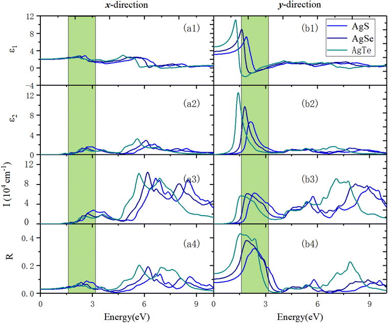
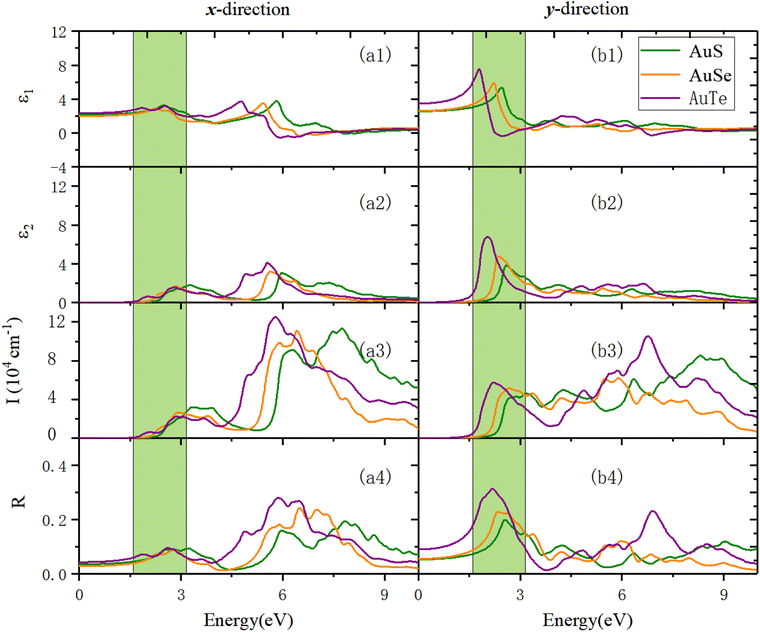
Fig. 11 shows the optical properties of β-AgX along the x- and y-directions. We can see that along the x-direction, in terms of absorption properties, the absorption edges of AgS, AgSe, and AgTe are 1.81 eV, 1.42 eV, and 1.20 eV, respectively. Their first optical absorption peaks are at 2.75 eV, 2.45 eV, and 2.28 eV. Before that, there is a shoulder peak at 2.11 eV, 1.77 eV, and 1.40 eV. The highest optical absorption coefficients in the visible (VIS) light region are 2.82 × 104 cm−1 (3.09 eV), 2.06 × 104 cm−1 (2.75 eV), and 1.51 × 104 cm−1 (2.68 eV). The prominent optical absorption peaks are all in the ultraviolet (UV) light region. The maximum absorption peaks in the UV light region are 6.65 eV (9.23 × 104 cm−1), 6.19 eV (1.05 × 105 cm−1), and 5.70 eV (1.02 × 105 cm−1) (Fig. 11(a3)). In terms of the optical reflection properties, the static reflection rates are 2.83%, 3%, and 3.12%, respectively. The first reflection peaks are located at 2.00 eV (5.53%), 2.34 eV (7.84%), and 1.30 eV (4.25%). In the VIS light region, the maximum reflection peaks are located at 2.67 eV (8.85%), 1.6628 eV (4.87%), and 2.18 eV (7.12%). The reflection coefficients in the UV light region are significantly increased. The maximum reflection peaks in the UV light range are 6.65 eV (14%), 6.22 eV (19.12%), and 5.72 eV (20.36%) (Fig. 11(a4)).
Along the y-direction, in terms of the optical absorption properties, the absorption edges of the three materials are 1.31 eV, 1.03 eV, and 0.72 eV, respectively. Their first absorption peaks are located at 2.36 eV (6.22 × 104 cm−1), 1.94 eV (6.13 × 104 cm−1), and 1.58 eV (5.68 × 104 cm−1). The maximum absorption coefficients in the VIS light region are all lower than the peak value of the first absorption peak. The maximum absorption peaks are all in the UV light region, located at 9.01 eV (7.50 × 104 cm−1), 8.20 eV (8.09 × 104 cm−1), and 7.09 eV (9.11 × 104 cm−1), respectively (Fig. 11(b3)). In terms of the reflection properties, the static reflection rates are 7.78%, 10.33%, and 14.15%, respectively. The first reflection peaks are the same as the maximum reflection peaks, located at 2.36 eV (32.23%), 1.91 eV (38.09%), and 1.55 eV (42.98%), respectively. The reflection coefficients in the UV light region are significantly reduced (Fig. 11(b4)).
Fig. 12 reveals the optical properties of β-AuX along the x- and y-directions. Panel (a3) in Fig. 12 exhibits the optical absorption properties in the x-direction. We can find that the absorption edges of AuS, AuSe, and AuTe are 2.14 eV, 1.92 eV, and 1.66 eV, respectively. The first absorption peaks of AuS, AuSe, and AuTe are located at 3.33 eV, 2.93 eV, and 2.87 eV. Before that, a shoulder peak exists in the region with smaller photon energy, and this shoulder peak becomes more and more evident as X changes from S to Te, accompanied by a red-shift. The absorption coefficients in the VIS light region are all less than 3 × 104 cm−1, and the prominent absorption peaks are all located in the UV light region. In the UV light region, the maximum absorption peaks are located at 7.75 eV (1.13 × 105 cm−1), 6.42 eV (1.11 × 105 cm−1), and 5.81 eV (1.25 × 105 cm−1), respectively. Panel (a4) in Fig. 12 shows the reflection properties of β-AuX along the x-direction. The static reflectivities are 3.6%, 2.9%, and 4.3%, respectively. The first reflection peaks are located at 2.54 eV (8.99%), 2.28 eV (7.45%), and 1.87 eV (7.24%). The maximum reflection peak values in the VIS light region are all less than 9.64%. The reflection coefficients in the UV light region are significantly increased. In the UV light region, the maximum reflection peaks are located at 7.84 eV (19.38%), 6.50 eV (24.24%), and 5.89 eV (28.02%), respectively.
Panels (b3) and (b4) in Fig. 12 show the optical absorption and reflection properties of β-AuX in the y-direction. In terms of the absorption properties, the absorption edges of the three materials are 1.80 eV, 1.46 eV, and 1.13 eV, respectively. The first optical absorption peaks are located at 2.90 eV (4.28 × 104 cm−1), 2.69 eV (5.18 × 104 cm−1), and 2.23 eV (5.77 × 104 cm−1). The absorption coefficients in the visible light region are all less than 5.77 × 104 cm−1, and the maximum optical absorption peaks are all located in the UV light region. They are 8.31 eV (8.52 × 104 cm−1), 5.89 eV (6.21 × 104 cm−1), and 6.78 eV (10.51 × 105 cm−1), respectively. As for the reflection properties, the static reflectivities are 5.38%, 5.58%, and 9.06%, respectively. The first reflection peaks are the same as the maximum reflection peaks, located at 2.56 eV (19.91%), 2.36 eV (22.85%), and 2.20 eV (31.34%). The optical reflection coefficients in the UV light region are distinctly reduced.
Generally, the primary absorption and reflection regions of β-NX along the x-direction are all in the UV light region, much higher in wavelength than the VIS and infrared (IR) light regions. The materials have good light transmittance along this direction in the VIS/IR light region. Meanwhile along the y-direction, their absorption capacity in the VIS light region increases significantly. The difference in absorption capacity in the UV light region is significantly reduced compared with that along the x-direction, and the central light reflection region is in the VIS light region. Along the y-direction, the materials have good transparency in the IR light region, and their light transmittance in the VIS light region is weaker than in the x-direction. The optical properties of the β-NX materials show strong anisotropy along different directions. In the future, they could have good application value in the nano-optoelectronic fields, with uses in solar cells, polarizers, LEDs, catalysis, and sensors, for example.
4 Conclusions
By employing first-principles calculations, we have predicted five new NTMC semiconductor materials, β-NX (N = Au, Ag; X = S, Se, Te), with excellent stability, and electronic, transport, and optical properties. Our research illustrates that β-NX materials have good mechanical, dynamical, and thermal stability. Their chemical bonds are composed of partial ionic and covalent bonds, and they have a flexible quality. Additionally, the β-NX materials have a reasonable band gap, tiny electron effective mass, LPEs, strongly anisotropic hole mobility, and anisotropic carrier diffusion and transport. These characteristics make them promising for applications in FETs, logic circuits, and integrated circuits. Furthermore, the β-NX materials have high absorption coefficients, and their optical properties show strong anisotropy in different directions, making them promising for high-performance solar cells, polarizers, LEDs, catalysis, and sensors. Hence, the NTMC semiconductor β-NX is a highly anticipated type of 2D material in the fields of nano-electronics and nano-optoelectronics.Author contributions
Q.-Y. C.: carried out DFT calculations and prepared the manuscript; F.-J. H., Y.-F. Z., J.-Q. R., and F. L.: contributed to the discussion and made suggestions; K. X.: software; Y. H. and H. Y: project administration and funding acquisition. All authors have read and agreed to the published version of the manuscript.Conflicts of interest
There are no conflicts to declare.Acknowledgements
This research was funded by the National Natural Science Foundation of China (Grant No. 12164050), the Major Science and Technology Project of Precious Metal Materials Genetic Engineering in Yunnan Province (Grant No. 2019ZE001-1, No. 202002AB080001-6, and No. 2018IC058), the Program for Yunling Scholars in Yunnan Province, Program for Donglu Scholars in Yunnan University, Scientific Research Fund Project of Yunnan Provincial Education Department (No. 2022J0628), the Yunnan Fundamental Research Projects (Grant No. 202201AU070019 and No. 202201AU070036), the Introduction of Talents Projects (No. XJ20210018), the Special Basic Cooperative Research Programs of Yunnan Provincial Undergraduate Universities (Grant No. 202101BA070001-162 and No. 202101BA070001-175), and Yunnan Local Colleges Applied Basic Research Projects (No. 2019FH001(-077)). We acknowledge the Key Laboratory of Artificial Microstructures in Yunnan Higher Education Institutions for providing facilities and experimental support.References
- M. Chhowalla, H. S. Shin, G. Eda, L. J. Li, K. P. Loh and H. Zhang, Nat. Chem., 2013, 5, 263–275 CrossRef PubMed.
- X. Huang, Z. Zeng and H. Zhang, Chem. Soc. Rev., 2013, 42, 1934–1946 RSC.
- R. Lv, J. A. Robinson, R. E. Schaak, D. Sun, Y. Sun, T. E. Mallouk and M. Terrones, Acc. Chem. Res., 2015, 48, 56–64 CrossRef CAS PubMed.
- H. H. Huang, X. Fan, D. J. Singh and W. T. Zheng, Nanoscale, 2020, 12, 1247–1268 RSC.
- C. Tan and H. Zhang, Chem. Soc. Rev., 2015, 44, 2713–2731 RSC.
- M. Ye, D. Zhang and Y. Yap, Electronics, 2017, 6, 43 CrossRef.
- J. Chen, Q. Huang, H. Huang, L. Mao, M. Liu, X. Zhang and Y. Wei, Nanoscale, 2020, 12, 3574–3592 RSC.
- L. Liu, D. Zemlyanov and Y. P. Chen, 2D Mater., 2021, 8, 045033 CrossRef CAS.
- G. A. Ermolaev, K. V. Voronin, M. K. Tatmyshevskiy, A. B. Mazitov, A. S. Slavich, D. I. Yakubovsky, A. P. Tselin, M. S. Mironov, R. I. Romanov, A. M. Markeev, I. A. Kruglov, S. M. Novikov, A. A. Vyshnevyy, A. V. Arsenin and V. S. Volkov, Nanomaterials, 2021, 11, 3269 CrossRef CAS PubMed.
- J. Chen, Y. Wang, W. Xu, Y. Wen, G. H. Ryu, J. C. Grossman and J. H. Warner, ACS Nano, 2021, 15, 16748–16759 CrossRef CAS PubMed.
- R. Hao, Q.-L. Feng, X.-J. Wang, Y.-C. Zhang and K.-S. Li, Rare Met., 2022, 41, 1314–1322 CrossRef CAS.
- T. Jena, M. T. Hossain and P. K. Giri, J. Mater. Chem. C, 2021, 9, 16693–16708 RSC.
- M. Cattelan, C. J. Sayers, D. Wolverson and E. Carpene, 2D Mater., 2021, 8, 045036 CrossRef CAS.
- L. Pi, L. Li, K. Liu, Q. Zhang, H. Li and T. Zhai, Adv. Funct. Mater., 2019, 29, 1904932 CrossRef CAS.
- J. Li, S. Kolekar, Y. Xin, P. M. Coelho, K. Lasek, F. A. Nugera, H. R. Gutirrez and M. Batzill, Chem. Mater., 2021, 33, 8018–8027 CrossRef CAS.
- Y. Wang, L. Zhou, M. Zhong, Y. Liu, S. Xiao and J. He, Nano Res., 2022, 15, 3675–3694 CrossRef.
- S. Yin, W. Zhang, C. Tan, L. Chen, J. Chen, G. Li, H. Zhang, Y. Zhang, W. Wang and L. Li, J. Phys. Chem. C, 2021, 125, 16129–16135 CrossRef CAS.
- X. Zhang, G. Su, J. Lu, W. Yang, W. Zhuang, K. Han, X. Wang, Y. Wan, X. Yu and P. Yang, ACS Appl. Mater. Interfaces, 2021, 13, 43063–43074 CrossRef CAS PubMed.
- J. Chen, J. Zhou, W. Xu, Y. Wen, Y. Liu and J. H. Warner, Nano Lett., 2022, 22, 3289–3297 CrossRef CAS PubMed.
- Y. Gu, L. Zhang, H. Cai, L. Liang, C. Liu, A. Hoffman, Y. Yu, A. Houston, A. A. Puretzky, G. Duscher, P. D. Rack, C. M. Rouleau, X. Meng, M. Yoon, D. B. Geohegan and K. Xiao, ACS Nano, 2022, 16, 13900 CrossRef CAS PubMed.
- P. Jamdagni, A. Kumar, S. Srivastava, R. Pandey and K. Tankeshwar, Phys. Chem. Chem. Phys., 2022, 24, 22289–22297 RSC.
- Y. Ma, X. Gong, F. Xiao, Y. Liu and X. Ming, ACS Appl. Nano Mater., 2022, 5, 11519–11528 CrossRef CAS.
- M. Wei, J. Lian, Y. Zhang, C. Wang, Y. Wang and Z. Xu, npj 2D Mater. Appl., 2022, 6, 1 CrossRef CAS.
- P. L. Gong, F. Zhang, L. Li, B. Deng, H. Pan, L. F. Huang and X. Q. Shi, J. Phys.: Condens.Matter, 2019, 31, 395501 CrossRef CAS PubMed.
- L. F. E. Machogo, M. Mthimunye, R. K. Sithole, P. Tetyana, N. Phao, G. N. Ngubeni, M. Mlambo, P. S. Mduli, P. M. Shumbula and N. Moloto, New J. Chem., 2019, 43, 5773–5782 RSC.
- P. Bai, S. Guo, S. Zhang, H. Qu, W. Zhou and H. Zeng, J. Semicond., 2019, 40, 062004 CrossRef CAS.
- C. Tang, L. Zhang, C. Zhang, J. MacLeod, K. Ostrikov and A. Du, Nanoscale Horiz., 2020, 5, 366–371 RSC.
- Q.-K. Yin, C.-L. Yang, M.-S. Wang and X.-G. Ma, J. Mater. Chem. C, 2021, 9, 12231–12238 RSC.
- Q. Y. Xie, J. J. Ma, Q. Y. Liu, P. F. Liu, P. Zhang, K. W. Zhang and B. T. Wang, Phys. Chem. Chem. Phys., 2022, 24, 7303–7310 RSC.
- G. Kresse and J. Furthmuller, Phys. Rev. B: Condens. Matter Mater. Phys., 1996, 54, 11169–11186 CrossRef CAS PubMed.
- G. Kresse and D. Joubert, Phys. Rev. B: Condens. Matter Mater. Phys., 1999, 59, 1758–1775 CrossRef CAS.
- P. E. Blochl, Phys. Rev. B: Condens. Matter Mater. Phys., 1994, 50, 17953–17979 CrossRef PubMed.
- J. P. Perdew, K. Burke and M. Ernzerhof, Phys. Rev. Lett., 1996, 77, 3865–3868 CrossRef CAS PubMed.
- J. Heyd, G. E. Scuseria and M. Ernzerhof, J. Chem. Phys., 2003, 118, 8207–8215 CrossRef CAS.
- J. Heyd and G. E. Scuseria, J. Chem. Phys., 2004, 121, 1187–1192 CrossRef CAS PubMed.
- S. Zhang, S. Guo, Y. Huang, Z. Zhu, B. Cai, M. Xie, W. Zhou and H. Zeng, 2D Mater., 2017, 4, 015030 CrossRef.
- Y. Li, Y. Liao and Z. Chen, Angew. Chem., Int. Ed., 2014, 53, 7248–7252 CrossRef CAS PubMed.
- V. Wang, G. Tang, Y. C. Liu, R. T. Wang, H. Mizuseki, Y. Kawazoe, J. Nara and W. T. Geng, J. Phys. Chem. Lett., 2022, 13, 11581–11594 CrossRef CAS PubMed.
- M. E. Kilic and K.-R. Lee, Carbon, 2021, 174, 368–381 CrossRef CAS.
- M. E. Kilic and K.-R. Lee, Carbon, 2022, 195, 154–164 CrossRef CAS.
- M. E. Kilic and K.-R. Lee, Mater. Today Phys., 2022, 27, 100792 CrossRef CAS.
- M. E. Kilic and K.-R. Lee, Phys. Rev. Appl., 2022, 18, 014066 CrossRef CAS.
- M. E. Kilic and K.-R. Lee, Phys. Rev. Mater., 2021, 5, 065404 CrossRef CAS.
- A. D. Becke and K. E. Edgecombe, J. Chem. Phys., 1990, 92, 5397–5403 CrossRef CAS.
- B. Silvi and A. Savin, Nature, 1994, 371, 683–686 CrossRef CAS.
- L. De Santis and R. Resta, Surf. Sci., 2000, 450, 126–132 CrossRef CAS.
- Y. Liu, G. Yin, W. An, Y. Ke and R. Quhe, Nanotechnology, 2022, 33, 475701 CrossRef PubMed.
- M. Abboud, D. H. Ozbey, M. E. Kilic and E. Durgun, J. Phys. D: Appl. Phys., 2022, 55, 185302 CrossRef.
- R. J. Clements, J. C. Womack and C. K. Skylaris, Electron. Struct., 2020, 2, 027001 CrossRef CAS.
- A. Savin, O. Jepsen, J. Flad, O. K. Andersen, H. Preuss and H. G. von Schnering, Angew Chem. Int. Ed. Engl., 1992, 31, 187–188 CrossRef.
- M. Gajdos, K. Hummer, G. Kresse, J. Furthmller and F. Bechstedt, Phys. Rev. B: Condens. Matter Mater. Phys., 2006, 73, 045112 CrossRef.
| This journal is © The Royal Society of Chemistry 2023 |

