 Open Access Article
Ceria nanomaterials containing ytterbium: low and high concentration – luminescence analyzed in the near infrared region†
Sitshengisiwe Chemuraa,
Tim Schrumpfa,
Christina Günterb and
Michael U. Kumke *a
*a
aInstitute of Chemistry (Optical Sensing and Spectroscopy), University of Potsdam, Karl-Liebknecht-Str. 24-25, 14476 Potsdam, Germany. E-mail: kumke@uni-potsdam.de
bInstitute for Earth Sciences, University of Potsdam, Karl-Liebknecht-Str. 24-25, 14476 Potsdam, Germany
First published on 5th December 2023
Abstract
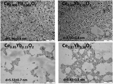
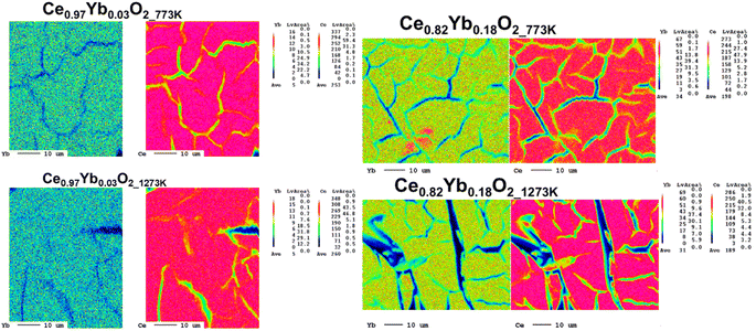
Lanthanide based ceria nanomaterials are important practical materials due to the redox properties that are useful in the avenues pertaining to technology and life sciences. Sub 10 nm spherical and highly monodisperse Ce1−xYbxO2−y (0.04 ≤ x ≤ 0.22) nanoparticles were synthesized by thermal decomposition, annealed separately at 773 K and 1273 K for 2 hours and characterized. Elemental mapping for Yb3+ doped ceria nanoparticles shows homogeneous distribution of Yb3+ atoms in the ceria with low Yb3+ content annealed at 773 K and 1273 K for 2 hours. However, clusters are observed for 773 K annealed ceria samples with high concentration of Yb3+. These clusters are not detected in 1273 K annealed nanomaterials. Introducing small amounts of Yb3+ ions into the ceria lattice as spectroscopic probes can provide detailed information about the atomic structure and local environments allowing the monitoring of small structural changes, such as clustering. The emission spectra observed at room temperature and at 4 K have a manifold of bands that corresponds to the 2F5/2 → 2F7/2 transition of Yb3+ ions. Some small shifts are observed in the Stark splitting pattern depending on the sample and the annealing conditions. The deconvolution by PARAFAC analysis yielded luminescence decay kinetics as well as the associated luminescence spectra of three species for each of the low Yb3+ doped ceria samples annealed at 773 K and one species for the 1273 K annealed samples. However, the ceria samples with high concentration of Yb3+ annealed at the two temperatures showed only one species with lower decay times as compared to the low Yb3+ doped ceria samples.
Introduction
Ceria, CeO2, is one of the most important materials in industrial applications: in solid oxide fuel cells, in biomedical applications, and as heterogeneous catalysts.1–5 Modifying the structure of pure CeO2 through doping (or mixing) with lanthanide ions (Ln3+) or tetravalent ions increases its lattice oxygen mobility. This in turn modifies the redox properties of the oxide.6,7 CeO2 can be easily altered by doping with other rare-earth ions for example Yb3+, because of their comparable ionic radii. Yb3+ has an ionic radius of 0.0985 nm which is close to that of Ce4+ (0.0970 nm) and Ce3+ (0.1143 nm).4,8–10 During the modification process of the crystal lattice, the incorporation of the Yb3+ or other lanthanides ions results in the Ce4+ ions substitution.1 The consequence is a one charge-compensating oxygen vacancy for every two trivalent dopants, resulting in multifaceted possible arrangements between Ce4+, Ln3+, O2− and oxygen vacancies.7,11,12 Yb3+ doped in nanomaterials finds many applications such as sensitizer in up-conversion and also as luminescence probe showing near infra-red (NIR) emission.13,14 Like other Ln3+ ions, Yb3+ can exhibit sharp luminescence bands via intra-4f or 4f–5d transitions.15 Taking advantage of this noble property, Yb3+ doped nanomaterials are an integral part of many lasers.16–19 With Yb3+ doping, highly desired imaging in the NIR spectral range is enabled which is otherwise hardly possible with other materials.1 The preferred oxidation state of ytterbium is +III (f13), but the +II (f14) can also be formed. Depending on its oxidation state f–f transitions or f–d-transitions can be observed. In complexes and solids Yb3+ ions can be found in different local symmetries, for example during formation of ceria, some of the Yb3+ ions substitute for the Ce ions and situate themselves in cubic (Oh), tetragonal (C4v), or trigonal C3v environments. These three sites can be accurately detected optically and only at very low dopant concentrations as there are no complex centers and defects in the lattices, which occur as a result of aggregates of Yb3+ ions when they are present in higher concentrations.20 Thus, at high concentrations an exclusive type of Yb3+ luminescent center is formed which dominates the emission. This has also been reported for CaF2:Yb3+ nanomaterials.21–23The Yb3+ ion has the electronic ground and excited states assigned to the 2F7/2 and 2F5/2 state, respectively.24,25 Depending on the crystal field, these can be further split into Stark level multiplets. At a low Cs symmetry, the ground state 2F7/2 can split into four and the excited state 2F5/2 into three Kramer's doublets.16,20,25–27 Thus, the transitions between the splitting levels are sensitive to the lattice site environment and also to the thermal vibration of crystal lattice occurring at room temperature and therefore thermal processes play a crucial part on the optical properties of the system.19,25,28
Trivalent rare-earth ions doped nanomaterials have a tendency to form cluster structures that contain at least two rare-earth ions in close environments and that are luminescence quenching centers.20 An additional luminescence quenching process can occur as a result of internal defects inside the oxide lattice, e.g., of CeO2, when Yb3+ are available in the lattice at high concentrations.1 Yb3+ clusters can likewise act as trapping centers resulting in a fast-non-radiative decay.29,30 Additionally, luminescence quenching takes place through cooperative luminescence between Yb3+–Yb3+ pairs. Annealing nanoparticles containing Yb3+ ions results in improved crystalline structure and to a greater extent eliminates quenching centers resulting in intensification of high temperature annealed samples' NIR emission.17 With the Gd2O3:Yb3+ phosphor, luminescence intensity was observed to become higher with increasing annealing temperature.27 This is envisaged to be due to lattice distortion which is eliminated by heating to a higher temperature and promoting crystallite growth, which in turn is responsible for the enhancement of NIR emission. Annealing Yb3+ doped CaF2 crystals in inert atmosphere also resulted in the reduction of Yb3+ to Yb2+ energy transfer and this also reported for BaZrO3:Yb3+ after a calcination at 1273 K.17
Upconversion luminescence has been used to track Yb3+ distribution in a ceria lattice incorporated with other lanthanide ions and corroborate the data from XRD and Raman on the formation of homogeneous solid solutions.29 In these materials, the down conversion luminescence of Yb3+ is seldom examined. Instead, the luminescence of the activator ions (Er3+, Tm3+ or Ho3+) is detected.
In this work, the luminescence of Yb3+ ions in ceria-based mixed oxides Ce1−xYbxO2 was investigated using time-resolved laser fluorescence spectroscopy (TRLFS). The dependence of the luminescence on the concentration of Yb3+ ions in ceria and on annealing temperatures was examined. The TRLFS experiments were carried out at room temperature and at 4 K (cryogenic conditions) in order to elucidate the distribution of Yb3+ ion in the ceria lattice, e.g., with respect the presence of lattice defects or to clustering.
Experimental section
Ce1−xYbxO2 nanomaterial synthesis
Thermal decomposition method was used to synthesize ceria nanoparticles doped (low content) or mixed (high content) with ytterbium. The protocol from Lee et al. was used with modifications.31 Briefly, ytterbium(III) nitrate pentahydrate, 99.9% (0.03 mmol; 0.0135 g), cerium(III) nitrate hexahydrate, 99.9% (0.97 mmol; 0.4212 g) were dissolved in oleylamine, technical grade, 70% (0.990 mL; 0.805 g) and 1-octadecene, technical grade, 90% (5 mL; 4 g). All chemicals were procured from Sigma-Aldrich and used without further purification. The mix proportions of ytterbium and cerium were varied according to the desired final product. The mixture was stirred (600 rpm and at 353 K) for 30 min under vacuum (∼50 mbar) until a clear brownish yellow solution was formed. Thereafter, it was heated to 533 K to react for 2 h. After cooling to room temperature, 80 mL acetone was added to the solution and the nanoparticles were collected by centrifugation (30 min; 4500 rpm) using an Eppendorf centrifuge (Model 5804, Eppendorf, Germany). The nanoparticles were redispersed in hexane (max. 3 mL). The nanoparticles were washed three more times in the same way and finally dispersed in 10 mL hexane and stored in the fridge for further analyses. To obtain a powder, the volumes of the nanoparticle solvent were reduced in a Heidolph rotary evaporator equipped to a Heidolph vacuum pump, before being dried in an oven at 353 K for an hour. The powders were calcined in air at 773 K and 1273 K for 2 h after that (in an oven MLM VEB Electro Bad Frankenhausen, WMW AG Maschinenbau, Germany).Ce1−xYbxO2 nanomaterial characterization
The powders were characterized by XRD, TEM, Raman spectroscopy, and TRLFS at room as well as ultra-low temperature. X-ray powder diffraction data were collected on a PANalytical Empyrean powder X-ray diffractometer in a Bragg–Brentano geometry. It is equipped with a PIXcel1D detector using Cu Kα radiation (λ = 1.54187 Å) operating at 40 kV and 40 mA. θ/θ scans were run in a 2θ range of 4–70° with step size of 0.0131° and a sample rotation time of 1 s. The diffractometer is equipped with a programmable divergence and anti-scatter slit, and a large Ni-beta filter. The detector was set to continuous mode with an active length of 3.0061°. The sizes of the crystallites were calculated using the Debye–Scherrer-equation:
 | (1) |
The lattice parameter a was calculated using the formulae:
 | (2) |
 | (3) |
Raman spectra were recorded to examine the lattice vibrations in the nanomaterials at room temperature with an excitation source of 633 nm laser using a Raman microscope (Witec, Alpha 300) with a grating of 2400 L mm−1 equipped with Andor DU401-BR-DD-352 CCD camera. 10× objective was used.
Scanning electron microscopy (SEM) and energy dispersive X-ray diffraction (EDXS) experiments were done on a JEOL JSM-6510 with a W-filament operated at 15 kV and equipped with an Oxford Instruments INCAx-act detector. Small amounts of the samples were deposited on a carbon glue pad. Prior to analysis, all samples were coated with 25 nm of carbon by vaporizing a thin carbon wire under extremely high temperatures in a vacuum chamber using a Polaron CC7650 Carbon Coater. The back scattered electron (BSE) detector was used for material contrast, the secondary electron (SEE) detector for topographic images at 15 kV. TEM measurements were done using a JEOL microscope (Model JEM 1011). The ImageJ software was used in the nanoparticle size calculation, for which 100 nanoparticles were considered in each case.
The time-resolved laser fluorescence spectroscopy (TRLFS) experiments were carried out using the box car method. The initial gate delay, Δt was set to 5 μs and the gate width was 100 μs using a slit width of 10 μm. Yb3+ ions were excited at λex = 915 nm. Fluorescence line narrowing spectroscopy measurements were accomplished by cooling samples contained in NMR tubes to T = 5 K using a closed cycle liquid helium cryostat. The cryostat is composed of a helium compressor unit (CKW-21, Sumitomo Heavy Industries Ltd.), a vacuum pump for the sample chamber (Turbolab 80, Oerlikon Leybold Vacuum), and a temperature controller (331, Lakeshore). A pulsed Nd:YAG laser (Quanta Ray, Spectra Physics, USA) with a set repetition rate of 10 Hz was coupled to an optical parametric oscillator (OPO, GWU Lasertechnik, Germany), serving as excitation light source. The excitation light was coupled into one of the branches of a Y-shaped fiber bundle, whereas the other branch was connected to a spectrograph (Kymera KY328i, Andor Technology, Oxford Instruments, equipped with a 300 L mm−1 grating) combined with an intensified charge-coupled device (iCCD) camera (iStar iCCD-06389, Andor Technology, Oxford Instruments). The time resolved emission data were analyzed by the parallel factor analysis (PARAFAC) algorithm, using MATLAB 2021b software (The MathWorks, Inc.).
The PARAFAC algorithm deconvolutes time delay and excitation dependent emission data based on the assumption that the total measured emission is the superposition of the weighted single species emission.32,33 This way it is possible to deconvolute the data into the luminescence decay kinetics and emission spectra of each ytterbium species. Deconvolution using a monoexponential constraint in the time dimension was done by the procedure described by.34 The term “species” describes groups of ytterbium ions located in identical lattice sites, yielding the same emission spectrum and decay kinetics. In case of a distribution with only minimal different lattice sites, PARAFAC will fuse those into a single species with an average emission spectrum or decay kinetics. The number of species present is judged by the core consistency value. The TRES results of the ceria–Yb mixed oxides samples are two-dimensional (delay-emission tensor) and were deconvoluted in one global function thus, no reasonable core consistencies were calculated in these cases.
Results and discussion
Basic characterization of Ce1−xYbxO2 nanomaterial
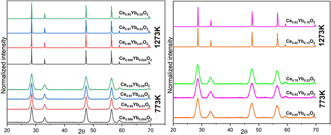 | ||
| Fig. 2 XRD patterns of the 773 K and 1273 K annealed Ce1−xYbxO2 nanomaterials (x = 0.004, 0.01, 0.03 and 0.05) (set 1, left) and for (x = 0.15, 0.18 and 0.22) (set 2, right). | ||
| Sample | Size (nm) | Peak position (°) | FWHM (°) | Lattice parameter (nm) | |||
|---|---|---|---|---|---|---|---|
| Annealing temperature | 773 K | 1273 K | 773 K | 1273 K | 773 K | 1273 K | |
| Ce0.996Yb0.004O2 | 12.4 ± 0.2 | 78.7 ± 2.3 | 28.57 ± 1.2 × 10⁻³ | 28.54 ± 6.1 × 10⁻⁴ | 0.73 ± 0.0029 | 0.14 ± 0.0015 | 0.5416 ± 1.8 × 10⁻⁴ |
| Ce0.99Yb0.01O2 | 12.5 ± 0.2 | 71.6 ± 1.8 | 28.60 ± 2.0 × 10⁻³ | 28.53 ± 6.4 × 10⁻⁴ | 1.42 ± 0.0048 | 0.15 ± 0.0015 | 0.5417 ± 1.8 × 10⁻⁴ |
| Ce0.97Yb0.03O2 | 12.4 ± 0.2 | 40.5 ± 1.0 | 28.56 ± 9.5 × 10⁻⁴ | 28.55 ± 5.4 × 10⁻⁴ | 0.73 ± 0.0023 | 0.16 ± 0.0013 | 0.5414 ± 2.5 × 10⁻⁴ |
| Ce0.95Yb0.05O2 | 9.4 ± 0.2 | 36.7 ± 0.7 | 28.56 ± 1.4 × 10⁻³ | 28.55 ± 5.1 × 10⁻⁴ | 1.02 ± 0.0033 | 0.17 ± 0.0012 | 0.5412 ± 2.1 × 10⁻⁴ |
| Ce0.85Yb0.15O2 | 8.0 ± 0.3 | 40.7 ± 0.6 | 28.58 ± 1.7 × 10⁻³ | 28.65 ± 3.3 × 10⁻⁴ | 1.29 ± 0.0041 | 0.18 ± 7.7 × 10⁻⁴ | — |
| Ce0.82Yb0.18O2 | 7.6 ± 0.3 | 40.0 ± 0.6 | 28.55 ± 1.1 × 10⁻³ | 28.67 ± 3.1 × 10⁻⁴ | 0.74 ± 0.0026 | 0.18 ± 7.4 × 10⁻⁴ | — |
| Ce0.78Yb0.22O2 | 8.0 ± 0.2 | — | 28.59 ± 1.6 × 10⁻³ | — | 1.24 ± 3.7 × 10⁻³ | — | — |
The lattice parameter for the lowest Yb3+ concentration (0.04 mol%) was calculated to be 0.5416 nm, but it varied from 0.5417 nm (for 1 mol% Yb–ceria) to 0.5412 nm (for 5 mol% Yb–ceria), as calculated from eqn (2) and (3). The difference in the lattice parameter shift can be directly related to the ionic radii of the dopant as compared to the host. There is a slight decrease in lattice parameter by introducing more Yb3+ ions in the host ion. The results are consistent with that observed by Babu et al. and supports that doping smaller trivalent ions e.g. Yb3+ (ionic radius 0.0985 nm) in ceria results in its lattice contraction. The extent of the lattice parameter change depends on the concentration of the trivalent dopant ion.35 Our results are also in line with what was observed by Giannici et al., where lattice contraction occurs with Yb3+ ion mixing into CeO2.36 However, Matović et al. observed an increase in the lattice parameters from a Yb3+ ions mixing concentration range of 5% to 20%.4
The effect of the higher annealing temperature on the samples is corroborated by the morphology results from SEM examinations (Fig. SI1†). No (significant) differences between set 1 and set 2 are found in XRD patterns, which indicate that no additional phase due to high Yb3+ ions content is formed or that would point to clustering of Yb3+ in the lattice.
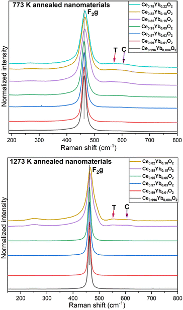 | ||
| Fig. 3 Raman spectra of ceria nanomaterials annealed at 773 K (top) and at 1273 K (bottom) with increasing Yb3+ concentration from 0.04 to 22 mol%. (λlaser = 633 nm). | ||
Four vibrational modes are observed in the Raman spectra. These are around 268, 464, 560, and 610 cm−1, respectively. The prominent peak at 464 cm−1 corresponds to the triply degenerate F2g Raman active mode of the fluorite structure. It is viewed as a symmetric breathing mode of the oxygen atoms around cerium ions.11 This peak is slightly blue shifted and becomes progressively broader (see FWHM in Table 2) and asymmetric with an increase in Yb3+ concentration. The intensity of the two modes that appear around 560 and 610 cm−1 (referred to as T and C respectively) gain intensity with increasing the Yb3+ concentration in the samples.
| Sample | FWHM (cm−1) | |
|---|---|---|
| Annealing temperature | 773 K | 1273 K |
| Ce0.996Yb0.004O2 | 20.5 ± 0.2 | 12.8 ± 0.1 |
| Ce0.99Yb0.01O2 | 20.6 ± 0.2 | 12.4 ± 0.1 |
| Ce0.97Yb0.03O2 | 22.3 ± 0.2 | 14.4 ± 0.1 |
| Ce0.95Yb0.05O2 | 26.6 ± 0.3 | 14.4 ± 0.1 |
| Ce0.85Yb0.15O2 | 42.0 ± 0.6 | 32.0 ± 0.4 |
| Ce0.82Yb0.18O2 | 42.0 ± 0.0 | 36.7 ± 0.4 |
| Ce0.78Yb0.22O2 | 41.2 ± 0.6 | — |
These defect modes are assigned to extrinsic vacancies induced by Yb3+ doping and the presence of Ce3+, respectively.3 As a consequence a substantial amount of oxygen vacancies due to charge compensation is introduced in the materials as the amount of Yb3+ increases as also reported by Florea et al.12 A very weak Raman mode around 268 cm−1 can be seen for the samples of set 2 heated at 773 K. Annealing at 1273 K intensifies this peak and result in the red shift of this mode to around 250 cm−1.
As shown in Table 1, annealing the nanomaterials at 1273 K promotes the increase in the crystalline size. This might lead to the noticeable decrease in the FWHM of the F2g peak of the Raman spectra with annealing temperature, as shown in Table 2 and Fig. 3 (bottom). A slight blue shift in the F2g peak is also observed with the higher calcination temperature.
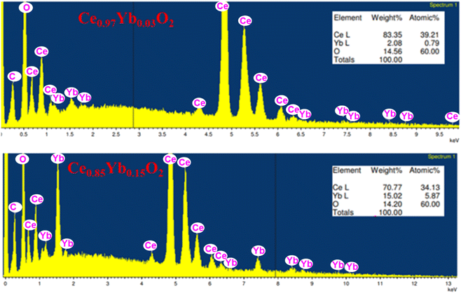 | ||
| Fig. 4 EDX spectrum and elemental composition chart for Ce0.97Yb0.03O2 and Ce0.85Yb0.15O2 annealed at 1273 K. | ||
Fig. 5 shows the elemental maps for Ce0.97Yb0.03O2 and Ce0.82Yb0.18O2 nanomaterials annealed at 773 K and 1273 K, respectively. Those for the Ce1−xYbxO2 (x = 0.04 and 0.15) nanomaterials are shown in the Fig. SI2.† The maps display homogeneous distribution of the ytterbium atoms in the ceria matrix for low Yb3+ contents (set 1 annealed at 773 K) and appear homogeneous for set 1 and 2 annealed at 1273 K. In case of set 2 samples annealed at 773 K high concentration areas are observed in some parts of the maps, which point to Yb3+ clusters. It is interesting to note that when the samples are annealed at 1273 K, the clusters are destroyed, which goes in line with the luminescence results (vide infra) and those obtained by Oliva et al.17 On the other hand, XRD did not indicate the formation of clusters.
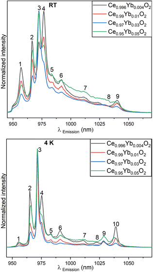
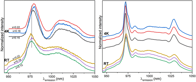
Nine broad peaks are observed at room temperature (top) in the NIR region (a list of peak position obtained from Gaussian fitting is given in the ESI†). The manifold corresponds to the Stark levels of the 2F5/2 → 2F7/2 transition of Yb3+ ions in different environments.19,27 There are two dominant peaks, the 972 nm and that around 976 nm. Based on the position of the emission lines, it can be hypothesized that the Yb3+ ions are located in C3v, and C4v symmetry environments, in the samples. These findings have been found in CaF2:Yb3+ samples.20–22 These symmetries are possible locations for Yb3+ ions in the ceria matrix due to defects sites or lattice distortions when the Yb3+ ions replace some of the cerium ions in the lattice. The intensity of the peak around 972 nm increases significantly as the concentration in Yb3+ increases from 1 to 5 mol%. The opposite happens with the intensity of the 976 nm peak. At room temperature, the homogeneous and inhomogeneous broadenings in the spectral emission are strong, thus the transition between sub-levels is not totally resolved especially for peaks in the high NIR wavelengths. Thermal vibrations within the lattice could also account for the background observed, but further analysis is needed to confirm its origin.
Fig. 6 (bottom) shows that at 4 K, the peaks in the emission spectra become sharper and better resolved as homogeneous and inhomogeneous broadenings are effectively reduced. The peaks at around 972 nm and around 1028 nm become more intense with cooling, especially for the lowest Yb3+ concentration containing sample. Also, the 976 nm peak intensity is effectively reduced as compared to the room temperature results. In comparison with the emission spectra at room temperature, the 972 nm is slightly red shifted and the 976 nm peak slightly blue shifted as a result of cooling. This can imply that as minor adjustments of the local environment around Yb3+ occur, polarizability of the ligands slightly change. It can be confirmed that the 976 nm peaks belong to the C3v symmetry.20,22 The small shifts observed are induced by the changes of the crystal field around the Yb3+ ions.
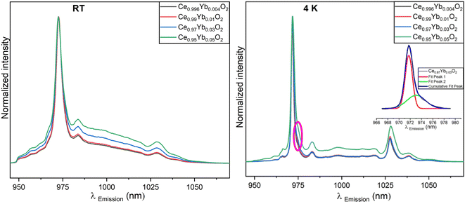
The emission spectra of Ce1−xYbxO2 nanocrystals (x ≤ 0.05) after annealing at 1273 K collected at room temperature (left) and at 4 K (right) are illustrated in Fig. 7. The shape of the emission spectra (e.g., number of emission peaks) changes with annealing temperature. At room temperature, the 972 nm peak is most prevalent and is observed along with two broad peaks as well as shoulder peaks between 950 nm and 970 nm. The most dominant peak is blue shifted and the FWHM increases with the increase of the Yb3+ ions amount (see Table 3). Lattice distortion is removed as crystallite growth is promoted with the higher annealing temperature resulting in the enhancement of the luminescence. Due to the position of the emission peaks and the Stark splitting pattern it is likely that the Yb3+ ions are located in C4v and C3v symmetry environments like in the room temperature results, although the peak positions are slightly shifted.20
| Sample | FWHM976 (nm) | FWHMdominant peak (nm) | ||
|---|---|---|---|---|
| RT_773 | 4 K_773 | RT_1273 | 4 K_1273 | |
| Ce0.996Yb0.004O2 | — | — | 5.8 ± 0.1 | 1.8 ± 0.0 |
| Ce0.99Yb0.01O2 | — | — | 6.1 ± 0.1 | 2.0 ± 0.0 |
| Ce0.97Yb0.03O2 | — | — | 7.4 ± 0.2 | 2.1 ± 0.0 |
| Ce0.95Yb0.05O2 | — | — | 9.3 ± 0.3 | 3.0 ± 0.8 |
| Ce0.85Yb0.15O2 | 12.1 ± 0.6 | 12.4 ± 0.2 | 4.5 ± 0.1 | 3.9 ± 0.2 |
| Ce0.82Yb0.18O2 | 15.7 ± 0.7 | 12.7 ± 0.1 | 4.7 ± 0.1 | 3.9 ± 0.2 |
| Ce0.78Yb0.22O2 | 16.7 ± 1.1 | 12.8 ± 0.1 | 4.8 ± 0.2 | 4.5 ± 0.3 |
The emission spectra of 1273 K annealed samples measured at 4 K again show sharper peaks compared to the spectra measured at room temperature (see Fig. 7, right). This is because the processes contributing to the spectral broadening of electronic transitions are reduced. The main feature in the emission spectra is the relatively sharp band around 972 nm. This peak is blue shifted with the increase in the Yb3+ ion concentration and red shifted with respect to the room temperature data. Although the peaks are narrower than those from room temperature measurements, it is still observed that there is an increase in the FWHM, with an increase in the concentration of Yb3+ ions (vide infra). Also, the 1028 nm peak is red shifted as the concentration of the Yb3+ ions increase in the samples. This may be a result of a mild modification of the local environment around Yb3+.37 The peaks around 967 nm are better resolved, too (see Fig. 7, left and right, respectively). There appears to be a shoulder around 976 nm (circled) that is protruding especially for samples with 0.4, 1 and 3 mol% Yb3+ ions. The Gauss deconvoluted fit for Ce0.97Yb0.03O2 displayed as an inset in Fig. 7 (right) shows that two sub-peaks can be fitted in the original 972 nm peak. These curves have a maximum at 971.7 and 973 nm respectively.
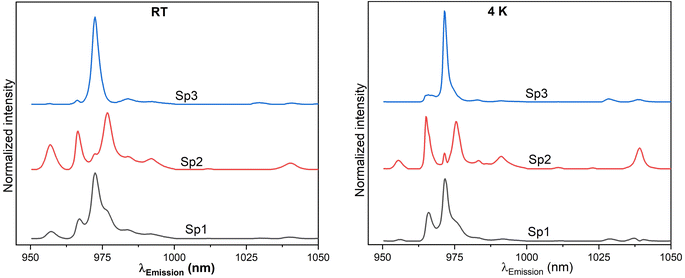
For room temperature three species were determined to be present in set 1 samples. The emission spectra are composed of broad peaks. The luminescence decay times for the species Sp1 and Sp2 are 583.2 μs and 1324.5 μs respectively. Species Sp3 has the least relative emission contribution and thus the determination of the respective decay time very inaccurate. Based on the emission peak pattern, Sp3 can be assigned to Yb3+ ions occupying a trigonal symmetry environment. On the other hand, for species Sp1 and Sp2 the C4v and C3v symmetries are assigned based on the location of emission peaks observed for CaF2:Yb3+ ceramics.21–23,38
Yb3+ ions in three different chemical environments are seen after cooling the samples to 4 K (Fig. 8, right) as well. The spectra display sharper, better resolved, and more intense signals compared to room temperature data. Moreover, the peaks also show a blue shift (as also seen in the raw data). Although, the spectrum from species Sp3 has a shoulder around 976 nm, the peaks around 1040 nm are well resolved and clearly seen. The luminescence decay time of species Sp2 is longest (1992.2 μs), which might be an indication for a slow rate of energy migration between the isolated Yb3+ ions.25 Sp1 has a decay time of 545.3 μs. Also, in this case the relative emission contribution of species Sp3 is low. However, as it is seen (vide infra), this species becomes the main species after annealing the nanomaterial samples at a higher temperature. As in the RT results, Yb3+ ions assigned to species Sp3 could be located in a C3v environment, while the other Yb3+ ions represented by species Sp2 and Sp1 are assigned with more confidence to C4v and C3v symmetry environments since they dominate in the luminescence.20,22 More research on the down conversion in ceria-based nanomaterials mixed with Yb3+ should be done to be able to confirm the assignment of the emission peaks in these materials.
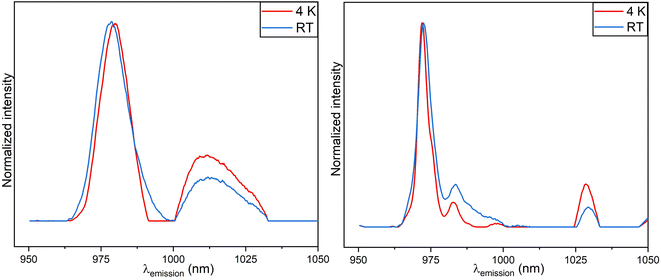
The emission spectra from PARAFAC results of room temperature and 4 K luminescence measurements of 1273 K annealed samples are shown in Fig. 9. PARAFAC deconvoluted RT data showed only one Yb3+ species present which portrays homogeneity and high crystallinity in the samples due to annealing at a higher temperature (see Fig. 9).
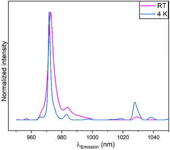 | ||
| Fig. 9 Emission spectra of room temperature and 4 K measured 1273 K annealed samples (set 1, x ≤ 0.05) obtained from PARAFAC analysis. | ||
A broad spectrum with a main peak centered around 972 nm is observed at room temperature together with a shoulder at ca. 967 nm and three more small peaks. The peaks become sharper with cooling to cryogenic conditions and the shoulder (in room temperature result that is around 967 nm) is well separated now into two peaks (although small) and the other peaks are also better resolved and more intense. Furthermore, the main peak is blue shifted. Also, upon cooling, the luminescence decay kinetics became slower indicated by the increased luminescence decay time (441.7 μs and 612.4 μs at RT and at 4 K respectively). For the samples annealed at 1273 K the Yb3+ ions are assumed to be in tetragonal and trigonal symmetry environments.22 Species Sp3 (RT, Fig. 8, left) and Sp3 (4 K, Fig. 8, right) of samples annealed at 773 K PARAFAC analysis yielded an emission profile which resembles that for single species found in the 1273 K annealed samples.
Annealing the nanomaterials at 1273 K results in the spectral signature changes as new peaks emerge at (983 and 1028 nm), with the most prevalent peak around 972 nm, all becoming slightly sharper after cooling to cryogenic conditions. The peaks also become well separated and a shoulder peak around 976 nm is observed, which is also observed for set 1 heated at 1273 K and the emission measured after cooling to 4 K (vide supra). Also, cooling to 4 K induces a blue shift on the dominant peak. A shoulder around 976 nm at emission profiles for room temperature measured samples is seen. Overall, for this set of samples the Yb3+ ions are assumed to be located in low symmetry environments based on their emission data. In Table 3, the FWHM of the dominant peak of the oxides is shown. A decrease of the FWHM of the dominant peaks is observed after (i) annealing the oxides at 1273 K and (ii) after cooling down the samples to 4 K for the luminescence measurements.
PARAFAC deconvoluted data (room temperature as well as 4 K) for 773 K annealed samples (Fig. 11, left) reveal only one Yb3+ species. The determined emission spectra have a broad dominant 978 nm peak along with another broad smaller peak centered at around 1012 nm (very similar to the raw data). The emission profile resembles that of a hexameric cluster that has been identified for CaF2:Yb3+ crystals with high content of Yb3+ ions.20,22 The luminescence of this species is greatly quenched judged by its luminescence decay time of only 2 μs. This is due to cross-talk between excited Yb3+ in close vicinity leading to energy migration among Yb3+ ions.41 There is no significant change observed in the PARAFAC results analyzing the 4 K data, except a slight red shift of the dominant peak. Thus, it is seen that when concentrations are elevated, as opposed to set 1, samples show short luminescence decay times, signifying a turning point for Yb3+, shifting from singly isolated state to clusters.25 Therefore, it is only sensible to reiterate the fact put out by Tamrak et al. that as Yb3+ concentration increases, additional Yb3+–Yb3+ pairs are formed, promoting cluster formation thus plummeting the emission of single Yb3+ ions.27 The emission spectra of set 2 annealed at 1273 K obtained by PARAFAC analysis for luminescence measurements carried out at RT and at 4 K are displayed in Fig. 11 (right). For the oxides annealed at 1273 K also only one Yb3+ species was found. The dominant peak in RT data is slightly blue shifted and also becomes slightly sharper with cooling (FWHM = 6.0 nm at RT and 4.82 nm at 4 K). The shoulder peak found around 992 nm is better resolved after cooling. It should be stressed that with a higher annealing temperature, the peak that dominates as a result of the so called hexameric cluster, occurring at circa 979 nm in 773 K annealed samples disappears, paving way to another new dominant peak. This also indicates a rearrangement and a destruction of the clusters with a higher annealing temperature, which is in line with the EDX results (vide supra). The decay times for the samples change from 44.4 μs for RT measurements to 50.4 μs for 4 K measurements (which is also significantly higher than for 773 K annealed samples and a further indication that the energy transfer between Yb3+ ions is reduced). It is however, interesting to note that, although the concentration of Yb3+ ions are very different in Yb3+-doped ceria and ceria oxide nanomaterials with high Yb3+ concentration, the RT and 4 K luminescence spectral signatures of 1273 K annealed nanomaterials (Fig. 11, right) are similar to that from Fig. 9, depicting the similarity in the most dominant symmetry environment occurring for the Yb3+ ions.
Conclusions
Ce1−xYbxO2−y:Eu3+ (0.004 ≤ x ≤ 0.22) nanomaterials were synthesized by a thermal decomposition method, with the molar quantities supported by EDX analysis. The particle crystallites of the 773 K and 1273 K annealed nanomaterials are nano-sized and have a cubic fluorite structure with four Raman vibrational modes as revealed by the XRD data and Raman spectroscopy data, respectively. Elemental maps clearly show that cluster formation occurs with high Yb3+ ion concentration from 15 mol% in the ceria lattice. The emission spectra of the Ce1−xYbxO2−y:Eu3+ (0.004 ≤ x ≤ 0.05) nanoparticles observed for room temperature and 4 K show a manifold of luminescence bands that corresponds to the 2F5/2 → 2F7/2 transition of Yb3+ ions.Different emission spectral signatures are observed for Ce1−xYbxO2−y:Eu3+ (0.15 ≤ x ≤ 0.22) nanomaterials, although the 2F5/2 → 2F7/2 transition is still detected. The emission spectra comprise of two broad high background dominated peaks. Cooling the samples down to 4 K results in small shifts observed in the Stark splitting pattern. Annealing the nanomaterials at 1273 K changes the spectral signatures as new peaks emerge and all peaks become slightly sharper and better resolved after cooling to cryogenic conditions.
PARAFAC analysis was executed to extract different Yb3+ species from the time-resolved luminescence data collected at RT and 4 K for both low and high concentration Yb3+ samples. The deconvolution yielded luminescence decay kinetics as well as the associated luminescence spectra of three species for each of the low Yb3+ doped ceria samples annealed at 773 K but only one species for the 1273 K annealed samples. Decay kinetics after cooling the samples to 4 K resulted in species with the decay times of 545.3 μs and 1992 μs. Annealing the nanomaterials at 1273 K and measuring the decay kinetics of the species resulted in one species with a decay time of 441.7 μs and 612.4 μs at RT and 4 K, respectively. However, the high concentration Yb3+ ceria samples yielded only one species with a distinctly lower decay times as compared to the low Yb3+ ions doped ceria samples. Here, the annealing temperature had only a small influence. As supported by elemental mapping analysis, increasing Yb3+ concentration in the ceria oxides, from 15 mol% up, enhances cluster formation, thus reducing the emission of single Yb3+ ions. A notable increase (from 2 μs to 50 μs) in the luminescence decay time was found for set 2 samples annealed at 1273 K, which confirmed that with higher annealing temperatures clusters are removed.
On a balance of probabilities, with good data processing, the presented results on Yb3+ could be an adaptable and sensitive structural probe that can be used to probe samples in the NIR region that is effective in technical materials. Also, in conjunction with the PARAFAC algorithm, valuable deconvolution of the data observed in room temperature measurements and overall high-resolution data from 4 K measurements especially provide a distinction on the number of Yb3+ species in low and high concentration Yb3+ ceria samples, where many sites can contribute to the overall emission.
Author contributions
S. C. and M. U. K. conceived this project. T. S. and S. C. prepared the samples. S. C. and C. G. conducted the investigations and characterizations. S. C. and C. G. analysed the data. S. C. drafted the original manuscript. M. U. K. reviewed and edited the manuscript with contributions from all authors.Conflicts of interest
There are no conflicts to declare.Acknowledgements
Authors are grateful to Dr Sibylle Rüstig for help with TEM measurements and Sophie Dettmann for supporting with data processing. S. C. and M. U. K. are thankful to the Deutsche Forschungsgemeinschaft (DFG, German Research Foundation) for financial support (grant no. 450169704). M. U. K. greatly appreciates the financial support by the Federal Ministry for the Environment, Nature Conservation, Nuclear Safety and Consumer Protection (02E11860F). Publication was funded by the Deutsche Forschungsgemeinschaft (DFG, German Research Foundation) – grant no. 491466077.Notes and references
- A. E. D'Achille, R. Gonzalez-Rodriguez, E. Campbell, B. H. Lee, J. L. Coffer and A. V. Naumov, ACS Biomater. Sci. Eng., 2020, 6, 6971–6980 CrossRef PubMed.
- B. Choudhury, P. Chetri and A. Choudhury, J. Exp. Nanosci., 2015, 10, 103–114 CrossRef CAS.
- D. Avram, I. Porosnicu, B. Cojocaru, M. Florea and C. Tiseanu, J. Lumin., 2016, 179, 265–271 CrossRef CAS.
- B. Matović, M. Stojmenović, J. Pantić, A. Varela, M. Žunić, N. Jiraborvornpongsa and T. Yano, J. Asian Ceram. Soc., 2014, 2, 117–122 CrossRef.
- C. Walkey, S. Das, S. Seal, J. Erlichman, K. Heckman, L. Ghibelli, E. Traversa, J. F. McGinnis and W. T. Self, Environ. Sci.: Nano, 2015, 2, 33–53 RSC.
- Y. Li, Y. Li, H. Wang and R. Liu, ACS Appl. Mater. Interfaces, 2021, 13, 13968–13977 CrossRef CAS PubMed.
- M. A. Małecka, CrystEngComm, 2017, 19, 6199–6207 RSC.
- D. Han, Y. Yang, F. Gu and Z. Wang, J. Alloys Compd., 2016, 656, 524–529 CrossRef CAS.
- C. L. Muhich, J. Phys. Chem. C, 2017, 121, 8052–8059 CrossRef CAS.
- A. Kumar, S. Babu, A. S. Karakoti, A. Schulte and S. Seal, Langmuir, 2009, 25, 10998–11007 CrossRef CAS PubMed.
- S. Chemura, T. Haubitz, P. A. Primus, M. Underberg, T. Hülser and M. U. Kumke, J. Phys. Chem. A, 2020, 124, 4972–4983 CrossRef CAS PubMed.
- M. Florea, D. Avram, V. A. Maraloiu, B. Cojocaru and C. Tiseanu, Nanoscale, 2018, 10, 18043–18054 RSC.
- G. Boulon, J. Alloys Compd., 2008, 451, 1–11 CrossRef CAS.
- L. Liu, J. Xing, F. Shang and G. Chen, Opt. Commun., 2021, 490, 126944 CrossRef CAS.
- J. Chen and J. X. Zhao, Sensors, 2012, 12, 2414–2435 CrossRef CAS PubMed.
- A. Kaminska, J. Cybińska, Y. Zhydachevskii, P. Sybilski, G. Meyer and A. Suchocki, J. Alloys Compd., 2011, 509, 7993–7997 CrossRef CAS.
- J. Oliva, E. De la Rosa, L. Diaz-Torres, P. Salas and C. Ángeles-Chavez, J. Appl. Phys., 2008, 104, 023505 CrossRef.
- H. Zhang, Z.-H. Chen, X. Liu and F. Zhang, Nano Res., 2020, 13, 1795–1809 CrossRef CAS.
- Z. Zou, Y. He, H. Yu, S. Pang, Y. Wu, J. Liu and L. Su, Opt. Mater. Express, 2018, 8, 1747–1753 CrossRef CAS.
- V. Petit, P. Camy, J.-L. Doualan, X. Portier and R. Moncorgé, Phys. Rev. B: Condens. Matter Mater. Phys., 2008, 78, 085131 CrossRef.
- Y. K. Voron'Ko, V. Osiko and I. Shcherbakov, J. Exp. Theor. Phys., 1969, 29, 86–90 Search PubMed.
- T. Kallel, M. A. Hassairi, M. Dammak, A. Lyberis, P. Gredin and M. Mortier, J. Alloys Compd., 2014, 584, 261–268 CrossRef CAS.
- J. Kirton and S. McLaughlan, Phys. Rev., 1967, 155, 279 CrossRef CAS.
- W.-P. Qin, Z.-Y. Liu, C.-N. Sin, C.-F. Wu, G.-S. Qin, Z. Chen and K.-Z. Zheng, Light: Sci. Appl., 2014, 3, e193 CrossRef CAS.
- S. Mei, J. Zhou, H. T. Sun, Y. Cai, L. D. Sun, D. Jin and C. H. Yan, Adv. Sci., 2021, 8, 2003325 CrossRef CAS PubMed.
- G. Lakshminarayana, H. Yang, S. Ye, Y. Liu and J. Qiu, J. Phys. D: Appl. Phys., 2008, 41, 175111 CrossRef.
- R. K. Tamrakar, D. Bisen, K. Upadhyay, I. P. Sahu and N. Brahme, J. Opt., 2015, 44, 337–345 CrossRef.
- E. Montoya, J. Sanz-García and L. Bausa, Spectrochim. Acta, Part A, 1998, 54, 2081–2085 CrossRef.
- Z. Chen, W. Gong, T. Chen, S. Li, D. Wang and Q. Wang, Mater. Lett., 2012, 68, 137–139 CrossRef CAS.
- J.-H. Cho, M. Bass, S. Babu, J. M. Dowding, W. T. Self and S. Seal, J. Lumin., 2012, 132, 743–749 CrossRef CAS.
- S. S. Lee, W. Song, M. Cho, H. L. Puppala, P. Nguyen, H. Zhu, L. Segatori and V. L. Colvin, ACS Nano, 2013, 7, 9693–9703 CrossRef CAS PubMed.
- R. Bro and C. A. Andersson, Chemometr. Intell. Lab. Syst., 1998, 42, 105–113 CrossRef CAS.
- C. A. Andersson and R. Bro, Chemometr. Intell. Lab. Syst., 2000, 52, 1–4 CrossRef CAS.
- B. Drobot, R. Steudtner, J. Raff, G. Geipel, V. Brendler and S. Tsushima, Chem. Sci., 2015, 6, 964–972 RSC.
- S. Babu, R. Thanneeru, T. Inerbaev, R. Day, A. E. Masunov, A. Schulte and S. Seal, Nanotechnology, 2009, 20, 085713 CrossRef PubMed.
- F. Giannici, G. Gregori, C. Aliotta, A. Longo, J. Maier and A. Martorana, Chem. Mater., 2014, 26, 5994–6006 CrossRef CAS.
- F. Wang, L. Hu, W. Xu, M. Wang, S. Feng, J. Ren, L. Zhang, D. Chen, N. Ollier and G. Gao, Opt. Express, 2017, 25, 25960–25969 CrossRef CAS PubMed.
- M. Ito, C. Goutaudier, Y. Guyot, K. Lebbou, T. Fukuda and G. Boulon, J. Phys.: Condens. Matter, 2004, 16, 1501 CrossRef CAS.
- Q. Zhang and X. Liang, J. Soc. Inf. Disp., 2008, 16, 755–758 CrossRef CAS.
- L. Xia, C. Yu, S. Sun, Q. Zhou, F. Wang, S. Wang, L. Hu, Q. Yang and Y. Zhang, Opt. Mater., 2019, 98, 109352 CrossRef CAS.
- J. Li, J. Zhang, Z. Hao, X. Zhang, J. Zhao and Y. Luo, Appl. Phys. Lett., 2012, 101, 121905 CrossRef.
Footnote |
| † Electronic supplementary information (ESI) available: SEM images and additional TEM images (SI1 and SI2). See DOI: https://doi.org/10.1039/d3ra06868d |
| This journal is © The Royal Society of Chemistry 2023 |

