DOI:
10.1039/D3RA07237A
(Paper)
RSC Adv., 2023,
13, 35018-35025
Interlayer coupling controlled electronic and magnetic properties of two-dimensional VOCl2/PtTe2 van der Waals heterostructure
Received
24th October 2023
, Accepted 26th November 2023
First published on 1st December 2023
Abstract
The coupling of hetero monolayers into van der Waals (vdW) heterostructures has become an effective way to obtain tunable physical and chemical properties of two dimensional (2D) materials. In this work, based on first principles calculations, we systematically explore the electronic and magnetic properties of a 2D VOCl2/PtTe2 heterostructure. Our results indicate that the ground state of the VOCl2/PtTe2 heterostructure is a ferromagnetic (FM) metal with large magnetic anisotropy energy, among which, the VOCl2 “sublayer” shows FM half metallic properties while the PtTe2 “sublayer” shows nonmagnetic metallic properties. The Curie temperature (TC) of VOCl2/PtTe2 is 111 K. Moreover, the FM–antiferromagnetic (AFM) phase transition can be obtained under biaxial strain. Our work provides an effective way to improve the performance of 2D monolayers in nano-electronic devices.
Introduction
Compared to conventional electronics based on charge, spintronics, also called spin transport electronics or spin-based electronics, have drawn great attention due to their coupling control of charge and spin,1–4 in which the electron spin carries information and offers opportunities for a new platform of designing devices combining standard microelectronics with spin-dependent effects that arise from the interaction between the spin of the carrier and the magnetic properties of the material. Since the discovery of graphene, two dimensional (2D) materials have been a booming topic in recent decades, such as transition metal dichalcogenides (TMDs), phosphorus, silicene, borophene, etc.5–7 However, most of the 2D materials are nonmagnetic, which hinders their application in spintronic devices due to the lack of spin degrees of freedom. Therefore, searching for 2D materials with intrinsic magnetism is an urgent need. Fortunately, the field is evolving rapidly and many exciting developments in 2D materials science have occurred, and the rise of ferromagnetic (FM) or antiferromagnetic (AFM) candidates has provided one new platform for the applications of 2D spintronics at the nanoscale. Since the exfoliation of the ferromagnetic (FM) CrI3 monolayer8 and Cr2Ge2Te6 monolayer9 from their van der Waals bulks in 2017, a number of 2D magnetic materials have been synthesized experimentally or predicted theoretically to date, such as TMDs or trichalcogenides MXi (M = Cr, Mn, Ni, Ru; X = Cr, Br, I; i = 2, 3),10–21 MPX3 (M = Fe, Ni, Mn, Co, Zn; X = S, Se),22–27 MOX (M = Fe, Cr, V, Ti; X = Cl, Br, I),28,29 and TM borides TMxBy (x, y = 1, 2; y = 3, 4, 6),30–32 etc., which display rich magnetic configurations, magnetoelectric coupling effects, and magnetoresistance properties.
However, the potential application of 2D magnetic materials in practical electronic devices still faces two main challenges; one is that the categories of 2D materials with intrinsic FM or AFM properties are rare. The other one is that the Curie temperature (TC) or Néel temperature (TN) of these 2D magnetic materials are far lower than room temperature, which impedes their application in spintronic devices. For examples, the TCs for the FM CrI3 monolayer, bilayer Cr2Ge2Te6 and Fe3GeTe2 monolayer are only 45 K, 40 K and 130 K, respectively. On the other hand, 2D AFM candidates are much more common in nature, which has become the complements of FM based spintronic devices due to their advantages that AFM materials are insensitive to external magnetic field and more common in reality,33 which enable them to be promising in practical application. However, one difficulty towards the application of 2D AFM candidates in spintronics is the vanishing of macroscopic magnetic moments in conventional antiferromagnets, which induces unpolarized conduction electrons. Thus, the generation of high spin polarization states in 2D antiferromagnets provides new opportunities to improve their performance in spintronics.
To date, many efforts regarding the precise regulation of spin configurations of 2D materials have been made, and various approaches have been proposed, such as applying electric field,16,34 exerting external strains,35–37 doping,38–41 and constructing heterostructure,42–45 and so on. Especially, the heterostructure engineering has become popular in recent years due to its valid regulation without extra consumption. For example, in 2022, Guo et al. revealed that the magnetic phase of monolayer NiI2 can undergo the switching of AFM state to FM state by reversing the polarization direction of ferroelectric In2Se3 layer, which leads to the spin-polarized/unpolarized current in the FM/AFM state.46 Yang et al. found that when the layers of the GaN increase, the band alignment of CrBr3/GaN heterostructure can be transformed from type-I to type-II.47 In 2023, Guo et al. demonstrated that the magnetic state of MnPS3/MnCl3 can be changed from AFM to FM by reducing the interlayer distance, and the electronic properties can also be modulated by the interlayer distance.48 Nonetheless, people's efforts to manipulate the spins states of AFM materials are rare.
In this work, we systematically studied the structure, electronic and magnetic properties of 2D VOCl2/PtTe2 heterostructure composed of AFM VOCl2 semiconductor and nonmagnetic PtTe2 semiconductor. Compared to VOCl2 monolayer and PtTe2 monolayer, the VOCl2/PtTe2 heterostructure is changed to be FM metal, in which the VOCl2 “sublayer” shows FM half metallic property, and PtTe2 “sublayer” shows NM metallic property. Moreover, the Curie temperature of FM VOCl2/PtTe2 is 111 K, and the magnetic anisotropy energy (MAE) of VOCl2/PtTe2 heterostructure is comparable with FeCo alloys. At last, we investigated the magnetic and electronic properties of VOCl2/PtTe2 heterostructure by applying biaxial strains, it is suggested that the heterostructure undergoes a FM metal to AFM metal transition, and the VOCl2/PtTe2 heterostructure can be used for designing field-effect spin filter under tensile strain and compressive strains (ε > −1.81%).
Materials and methods
All the calculations based on density functional theory (DFT) were performed by Vienna Ab initio Simulation Package (VASP) in this work.49–51 The exchange correlation interaction is described by Perdew–Burke–Ernzerholf (PBE)52 functional, and the interaction between valence electrons and ion nuclei is described by the projector-augmented wave potential (PAW)53 method. The cutoff value for plane wave basis set is set to 500 eV. The energy and force convergence criteria are set to be 10−6 eV and 0.01 eV Å−1, respectively. In our calculation, a vacuum slab as large as 25 Å is applied to avoid the physical interactions of adjacent cells. For geometry optimization and electronic structure calculations, the first Brillouin zone is sampled by Γ-centred k mesh of 7 × 7 × 1 and 15 × 15 × 1. The vdW interaction is considered by using the DFT-D2 method.54 In order to consider the strong interactions of transition metal atoms' d-electrons, the GGA + U method55 is adopted with Ueff = 3.0 eV to consider the Coulomb and exchange interaction of 3d electrons according to previous studies.56–58
Results and discussions
First, we explored the structures and electronic properties of VOCl2 and PtTe2 monolayers. As shown in Fig. 1(a) and (c), the space symmetry groups of VOCl2 and PtTe2 monolayers are Pmm2 and P3m1, respectively, and the lattice constants of them are a/b = 3.44/3.77 Å and a/b = 3.93/3.93 Å, respectively. For VOCl2 monolayer, the V and O atoms sit in one plane, which were sandwiched by two Cl layers, and Cl atoms are in the bridge site of V–V bonds. PtTe2 monolayer has the same structure with 1T-MoS2 monolayer. Further electronic and magnetic property calculations confirm that VOCl2 monolayer is stripe-style AFM semiconductor with an indirect band gap of 2.0 eV, and PtTe2 monolayer is a nonmagnetic semiconductor with an indirect band gap of 0.46 eV. The structure and electronic properties of both VOCl2 monolayer and PtTe2 monolayer in our calculation are consistent with previous reports,59,60 indicating that the methods chosen in this work are reasonable. To build the VOCl2/PtTe2 heterostructure, the rectangular lattice of PtTe2 with  supercell and 2 × 1 × 1 VOCl2 supercell are chosen. The optimized in-plane lattice constant of the heterostructure is 6.88 Å and 3.77 Å along a and b directions, which are same with that of 2 × 1 × 1 VOCl2 supercell. In addition, we calculated the lattice mismatch of PtTe2 monolayer based on
  Here, L1 and L represent the lattice constants of PtTe2 monolayer and the heterostructure in the same direction, respectively. The lattice mismatch along a and b directions for PtTe2 sublayer are about 1.16% and 3.98%, respectively, such mismatch is acceptable in 2D heterostructures.
 |
| | Fig. 1 (a and c) Top and side views of the geometry and band structure of VOCl2 monolayer and PtTe2 monolayer. The unitcell is denoted by the black arrows and the dotted lines. (b and d) The band structures of VOCl2 monolayer and PtTe2 monolayer, insets in (b) are the spin density plot of VOCl2 monolayer. | |
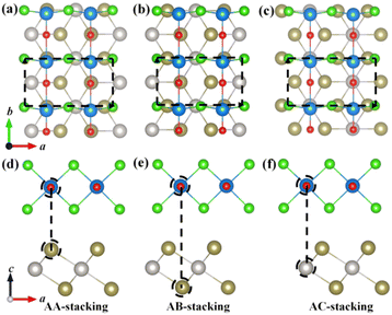
To determine the most stable stacking configuration of VOCl2/PtTe2 heterostructure, three different stacking styles, that is, AA-, AB-, and AC-stacking, were considered, as shown in the top and side views in Fig. 2. (i) AA-stacking: half of the V atoms in VOCl2 monolayer sit on top of Te atoms facing Cl atoms, as shown in Fig. 2(a) and (d); (ii) half of the V atoms in VOCl2 monolayer sit on top of Te atoms far away from the interface of the heterostructure, as shown in Fig. 2(b) and (e); (iii) half of the V atoms in VOCl2 monolayer sit on top of Pt atoms, as shown in Fig. 2(c) and (f). The results show that the AA stacking configuration is the most stable one, which is about of 0.51 eV per u.c. and 0.59 eV per u.c. lower in energy than that of AB- and AC-stacking configurations, respectively. The interlayer distance between VOCl2 monolayer and PtTe2 monolayer is 3.02 Å, indicating the van der Waals (vdW) interaction of the heterostructure. Based on this analysis, we will only focus on the electronic and magnetic properties of VOCl2/PtTe2 heterostructure with AA stacking in the following section.
 |
| | Fig. 2 (a–f) Top and side views of the AA-, AB-, and AC-stacked VOCl2/PtTe2 heterostructure. The black dotted circles in side view imply that the two atoms are overlapping in top view. | |
In order to verify the structural stability of the VOCl2/PtTe2 heterostructure, we calculated the binding energy (Eb) according to eqn (1),
| | |
Eb = EVOCl2/PtTe2 − EVOCl2 − EPtTe2,
| (1) |
where
EVOCl2/PtTe2,
EVOCl2 and
EPtTe2 represent the energy of VOCl
2/PtTe
2 heterostructure, VOCl
2 monolayer and PtTe
2 monolayer, respectively. The calculated binding energy is −0.52 eV, the negative value indicates that the VOCl
2/PtTe
2 heterostructure is energetically stable. Such stability of the VOCl
2/PtTe
2 heterostructure may arise from the interfacial electrons transfer between the two sublayers, which would occur in 2D vdW heterostructure. Therefore, the charge transfer at the heterostructure interface was examined by calculating the charge density difference (CDD) based on
eqn (2),
| | |
Δρ = ∫ρall(x, y, z) − ∫ρ1(x, y, z) − ∫ρ2(x, y, z),
| (2) |
here, the three terms on the right side indicate the charge densities of the VOCl
2/PtTe
2 heterostructure, VOCl
2 monolayer and PtTe
2 monolayer, respectively. The positive and negative values of Δ
ρ indicate charge accumulation and depletion, respectively. As shown in the inset of
Fig. 3(e), the charges are redistributed at the interface of the heterostructure. The plane-averaged charge density difference is plotted in the right panel in
Fig. 3(e), which has negative/positive charge densities near the PtTe
2/VOCl
2 interface, indicating the electron loss/gain of the two sublayers, which are transferred from PtTe
2 monolayer to VOCl
2 monolayer. In order to better understand interface charge transfer, we calculated the electrostatic potential (see
Fig. 3(e)). It can be seen that the potential of VOCl
2 monolayer is slightly higher (about 7.37 eV) than that of PtTe
2 monolayer, forming an effective electric field from VOCl
2 monolayer to PtTe
2 monolayer, which results in the fact that electrons transfer from PtTe
2 monolayer to VOCl
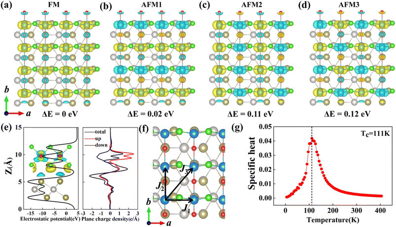
2 monolayer. Such results are consistent with that shown in the plane-averaged charge density difference, to determine the magnetic ground state of VOCl
2/PtTe
2 heterostructure, four types of magnetic configurations, that is, one ferromagnetic (FM) and three antiferromagnetic (AFM1, AFM2, AFM3) configurations are considered, as displayed in
Fig. 3(a)–(d). Our calculations show that the heterostructure favors FM ground state (see
Fig. 3(a)), which is about 0.02 eV, 0.11 eV, and 0.12 eV lower in energy than that of AFM1, AFM2, and AFM3 magnetic states. The spin density plot (
Fig. 3(a)) manifests that the magnetic moments of the heterostructure are contributed by the VOCl
2 sublayer, while the PtTe
2 sublayer is still nonmagnetic. The total magnetic moment of this VOCl
2/PtTe
2 heterostructure is 2.16
μB per unit cell, which arises mainly from the d orbitals of V atoms and p orbitals of Te atoms. Compared with free standing VOCl
2 monolayer, the O atoms goes closer to the middle of the two V atoms and the Cl atoms are closer to the V–O plane, resulting in a change in the V–O bonds from 2.28 Å/1.49 Å to 2.10 Å/1.67 Å, and a change in the V–Cl bonds from 2.67 Å to 2.38 Å, and the Cl–V–Cl bond angle is changed from 80.27° to 92.63°. According to the Goodenough–Kanamori–Anderson (GKA) rule,
61–63 super-exchange interaction with the angle between TM–B–TM close 90° favors FM magnetic ordering. In VOCl
2/PtTe
2 heterostructure, the V–Cl–V bond angle is 91.88°, which is closer to 90° than that in free standing VOCl
2 monolayer of 80.27°, such variation may strengthens the ferromagnetic coupling, leading to the FM ground state in the VOCl
2/PtTe
2 heterostructure. The Bader charge analysis shows that the average charges on V/O atom are 3.30 electrons and 6.78 electrons in the VOCl
2/PtTe
2 heterostructure, respectively, which are larger/smaller than that in free standing VOCl
2 monolayer of −0.11 e/0.20 e. Such electron redistribution of VOCl
2 monolayer originates from the interlayer interaction, as mentioned above, electrons transfer from PtTe
2 monolayer to VOCl
2 monolayer. The partially filled p orbitals in the O anions are responsible for the local magnetic moment of −0.158
μB and −0.172
μB in VOCl
2/PtTe
2 heterostructure.
 |
| | Fig. 3 (a–d) FM configuration and three AFM configurations. Yellow and blue colours represent up and down spins, respectively. (e) Electrostatic potential and plane-averaged charge density difference along the z-direction, inset in electrostatic potential is the CDD plot, black, red, and blue lines in plane-averaged charge density difference denote the total, spin-up, and spin-down charge densities, respectively. (f) Magnetic configuration for estimating the exchange-interaction constants of VOCl2/PtTe2 heterostructure. J1, J2 and J3 represents the intralayer and interlayer spin-exchange parameters. (g) The specific heat (CV) as a function of the temperature. | |
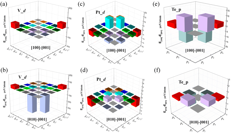
Next, we calculated the MAE to investigate the stability of the 2D FM order in the VOCl2/PtTe2 heterostructure. By considering spin orbital coupling (SOC), we calculated the energies of the heterostructure with magnetization along x, y and z positive directions. The results show that the system hosts the lowest energy when the magnetization is along the y axis, which is about 0.84 meV and 0.78 meV lower than that of along x and z axis positive directions, respectively, indicating the easy magnetization axis is in-plane and the MAE value is 0.84 meV, such MAE value is comparable with that in FeCo alloys, which is promising magnetic recording media.64 Fig. 4 shows the amount of energy change in the [100], [010] and [001] directions for individual V-d and Pt-d orbitals. It is revealed that the hybridization between V-dyz and dxy orbitals and that between V-dyz and V-dx2−y2 contribute mainly to the MAE. In addition, the energy changes of individual Pt-d and Te-p orbitals are within 15 μeV. Furthermore, we calculate the Curie temperature (TC) of FM VOCl2/PtTe2 heterostructure using Monte Carlo (MC) simulations based on the Heisenberg model, which is a critical characteristic regarding the application of 2D FM materials in spintronic devices. The Heisenberg spin Hamiltonian is written as
| |
 | (3) |
here,
Si is the spin operator of each V atom.
Ai is the MAE index.
Jk is the magnetic interaction index between the V atom. We consider the nearest neighbour (
J1), the second nearest neighbour (
J2), and the third nearest neighbour (
J3) (
Fig. 3(f)), whose values can be extracted from the following equations,
| | |
EFM = E0 − (J1 + J2 + 2J3)|S|2 − A|S|2
| (4) |
| | |
EAFM1 = E0 − (−J1 + J2 − 2J3)|S|2 − A|S|2
| (5) |
| | |
EAFM2 = E0 − (J1 − J2 − 2J3)|S|2 − A|S|2
| (6) |
| | |
EAFM3 = E0 − (−J1 − J2 + 2J3)|S|2 − A|S|2
| (7) |
 |
| | Fig. 4 The contribution to MAE from the SOC interaction between different V-d, Pt-d and Te-p orbital atoms along the [100] and the [010] directions. The energy is the reference along the [001] direction. | |
The exchange parameters (J1, J2 and J3) can be derived as:
| | |
J1 = −(EFM − EAFM1 + EAFM2 − EAFM3)/4|S|2
| (8) |
| | |
J2 = −(EFM + EAFM1 − EAFM2 − EAFM3)/4|S|2
| (9) |
| | |
J3 = −(EFM − EAFM1 − EAFM2 + EAFM3)/8|S|2
| (10) |
Here, the values of
J1,
J2 and
J3 are calculated to be 0.037 eV, 0.001 eV and 0.003 eV, respectively. In
Fig. 3(g), we further calculated the specific heat (
CV) as a function of the temperature from 0 K to 400 K. It is shown that the specific heat reaches a maximum at around 111 K and then decreases rapidly with the temperature further increases, indicating that the
TC of the heterostructure is about 111 K. It is known that VOCl
2 monolayer is AFM semiconductor with Néel temperature of 177 K based on Ising model,
59 which will overestimate the magnetic transition temperature. Therefore, it is believed that by forming VOCl
2/PtTe
2 heterostructure, an AFM-FM transition occurs and the magnetic transition temperature is almost unchanged.
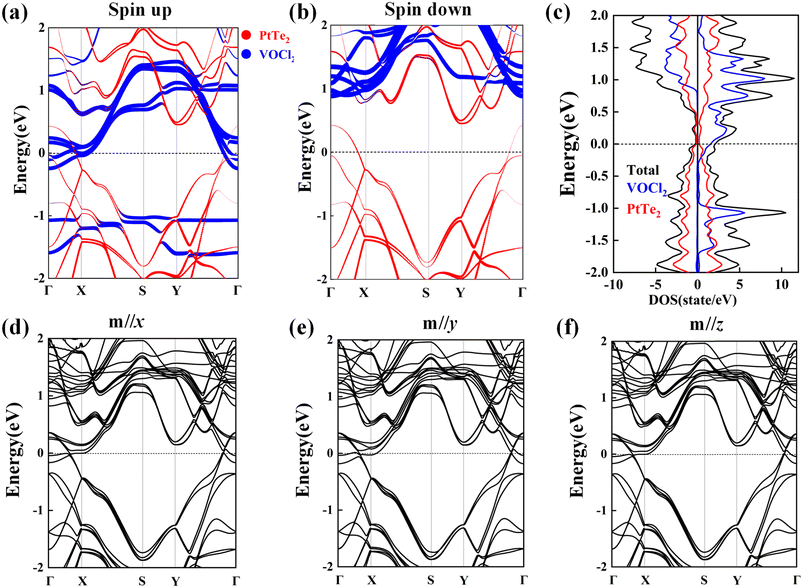
To explore the electronic properties of the structure, spin-polarized band structures of VOCl2/PtTe2 heterostructure are plotted in Fig. 5(a) and (b), and the heterostructure is revealed to be FM metal with bands in both spin channels crossing Fermi level. Specially, PtTe2 sublayer becomes to be nonmagnetic metal with the Fermi level down shifted, while VOCl2 sublayer is turned to be FM half metal, which the electrons are conducting in the spin-up channel and insulating in the spin-down channel. The density of states (DOS) of VOCl2/PtTe2 heterostructure is shown Fig. 5(c), which suggests that the states near the Fermi level are mainly from VOCl2 sublayer. Detailed orbital component analyses show that V-dxy and dyz orbitals contribute predominant. In addition, we calculate the band structures with different magnetization directions by including SOC effect, as shown in Fig. 5(d)–(f), which suggest that SOC effect has little effect on the electronic properties for VOCl2/PtTe2 heterostructure.
 |
| | Fig. 5 (a and b) Spin polarized band structures and (c) density of states (DOS) of VOCl2/PtTe2 heterostructure, in which the bands from PtTe2 and VOCl2 sublayers are denoted by red and blue lines, respectively. (d–f) Band structures of VOCl2/PtTe2 considering SOC effect with the magnetization direction along x, y, and z directions, respectively. | |
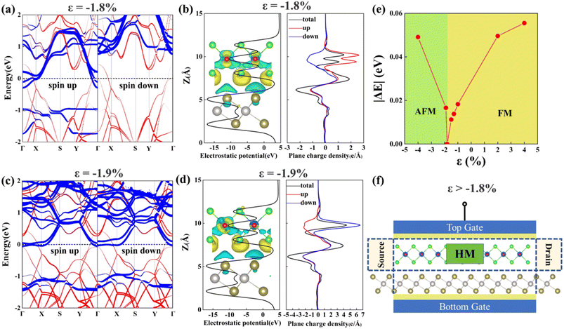
Finally, we discuss the effects of biaxial strains on the electronic and magnetic properties of VOCl2/PtTe2 heterostructure. We consider the strains from ε = −4% compressive strain to ε = 4% tensile strain, which is defined as ε = (L − L0)/L0, L and L0 are the lattice constants in freestanding and strained states, respectively. Our results indicate that the heterostructure remains FM ground state under biaxial tensile strains (ε > 0), but undergoes FM state to AFM state transition when applying biaxial compressive strains (ε < 0) at around 1.81% (see Fig. 6(e)). The spin polarized band structures of the VOCl2/PtTe2 heterostructure under 1.8% and 1.9% biaxial compressive strains around the phase transition point are depicted in Fig. 6(a) and (c). Clearly, the system remains FM metallic property at smaller compressive strain (ε > −1.81%), however, it changes to be AFM metal at higher strains (ε < −1.81%). To be specific, the “VOCl2” sublayer displays FM half metal property under smaller biaxial compressive strain (ε > −1.81%), which is transformed to be AFM metal under larger compressive strain (ε < −1.81%). Such transition may arise from the structure distortion under strains, which further lead to the variation in exchange interactions in the heterostructure. Fig. 6(b) and (d) plot the electrostatic potential and plane charge density of the heterostructure at biaxial compressive strains of −1.8% and −1.9%, respectively. It is shown that a bit smaller charge transfer is found in the interlayer of VOCl2/PtTe2 under larger compressive strain. Therefore, the VOCl2/PtTe2 heterostructure can be used to design a field-effect spin filter as shown in Fig. 6(f), we can obtain a fully spin-polarized current by using “VOCl2” sublayer when a non-spin-polarized current is input and the VOCl2/PtTe2 heterostructure is under tensile strain or compressive strains (ε > −1.81%). Thus, the heterostructure can be a potential candidate for application in electrically controlled spintronics device.
 |
| | Fig. 6 Spin-resolved band structures, electrostatic potential, and charge density along z direction for VOCl2/PtTe2 heterostructure under (a and b) 1.8% and (c and d) 1.9% biaxial compressive strains, respectively. The contributions from PtTe2 monolayer and VOCl2 monolayer are represented by red and blue colours, respectively. (e) Magnetic ground states of the VOCl2/PtTe2 heterostructure under different biaxial strains, where |ΔE| denotes the absolute value of the energy difference between the FM state and the lowest energy AFM state. (f) The schematic plot of the field-effect spin filter of the VOCl2/PtTe2 heterostructure. | |
Conclusions
In this work, we investigated the structure, magnetic, and electronic properties of two dimensional VOCl2/PtTe2 heterostructure by first-principles calculations. The results show that the VOCl2/PtTe2 heterostructure has FM ground state with the Curie temperature of about 111 K, higher than that of many 2D intrinsic FM materials. The band structure of the VOCl2/PtTe2 heterostructure is FM metal, in which the VOCl2 “sublayer” shows to be FM half metal, and PtTe2 “sublayer” shows to be nonmagnetic metal. Moreover, FM metal to AFM metal transition can be occurred by applying biaxial compressive strains larger than 1.81%. Our results provided an effective way on the property regulation of 2D electronic devices.
Author contributions
Conceptualization, Zhonghua Qian, Jie Ji and Licheng Wang; validation – Liyan Qian; formal analysis, Yuxuan Mao; data curation – Jie ji, Suchen Yao, and Jingyi Xu; writing – original draft preparation, Zhonghua Qian, Jie Ji; writing – original draft, supervision, Licheng Wang; review & editing, project administration, Xiuyun Zhang.
Conflicts of interest
There are no conflicts to declare.
Acknowledgements
This work is supported by the National Natural Science Foundation of China (41975062).
References
- S. A. Wolf, D. D. Awschalom, R. A. Buhrman, J. M. Daughton, S. von Molnar, M. L. Roukes, A. Y. Chtchelkanova and D. M. Treger, Science, 2001, 294, 1488–1495 CrossRef CAS PubMed.
- I. Zutic, J. Fabian and S. Das Sarma, Rev. Mod. Phys., 2004, 76, 323–410 CrossRef CAS.
- A. Fert, Rev. Mod. Phys., 2008, 80, 1517–1530 CrossRef CAS.
- S. D. Bader and S. S. P. Parkin, i, Annu. Rev. Condens. Matter Phys., 2010, 1, 71–88 CrossRef CAS.
- L. F. Wang, B. Wu, J. S. Chen, H. T. Liu, P. A. Hu and Y. Q. Liu, Adv. Mater., 2014, 26, 1559–1564 CrossRef CAS PubMed.
- Q. H. Wang, K. Kalantar-Zadeh, A. Kis, J. N. Coleman and M. S. Strano, Nat. Nanotechnol., 2012, 7, 699–712 CrossRef CAS PubMed.
- L. Li, F. Yang, G. J. Ye, Z. Zhang, Z. Zhu, W. Lou, X. Zhou, L. Li, K. Watanabe, T. Taniguchi, K. Chang, Y. Wang, X. H. Chen and Y. Zhang, Nat. Nanotechnol., 2016, 11, 593–597 CrossRef CAS PubMed.
- H. Wang, F. Fan, S. Zhu and H. Wu, Europhys. Lett., 2016, 114, 47001 CrossRef.
- K. Zollner, M. Gmitra and J. Fabian, New J. Phys., 2018, 20, 073007 CrossRef.
- Z. W. Zhang, J. Z. Shang, C. Y. Jiang, A. Rasmita, W. B. Gao and T. Yu, Nano Lett., 2019, 19, 3138–3142 CrossRef CAS PubMed.
- X. H. Cai, T. C. Song, N. P. Wilson, G. Clark, M. H. He, X. O. Zhang, T. Taniguchi, K. Watanabe, W. Yao, D. Xiao, M. A. McGuire, D. H. Cobden and X. D. Xu, Nano Lett., 2019, 19, 3993–3998 CrossRef CAS PubMed.
- E. Gerber, Y. Yao, T. A. Arias and E. A. Kim, Phys. Rev. Lett., 2020, 124, 106804 CrossRef CAS PubMed.
- W. O. Chen, Z. Y. Sun, Z. J. Wang, L. H. Gu, X. D. Xu, S. W. Wu and C. L. Gao, Science, 2019, 366, 983–987 CrossRef CAS PubMed.
- Y. J. Zhang, X. H. Wu, B. B. Lyu, M. H. Wu, S. X. Zhao, J. Y. Chen, M. Y. Jia, C. S. Zhang, L. Wang, X. W. Wang, Y. Z. Chen, J. W. Mei, T. Taniguchi, K. Watanabe, H. G. Yan, Q. H. Liu, L. Huang, Y. Zhao and M. Y. Huang, Nano Lett., 2020, 20, 729–734 CrossRef CAS PubMed.
- M. Abramchuk, S. Jaszewski, K. R. Metz, G. B. Osterhoudt, Y. P. Wang, K. S. Burch and F. Tafti, Adv. Mater., 2018, 30, 1801325 CrossRef PubMed.
- Y. J. Deng, Y. J. Yu, Y. C. Song, J. Z. Zhang, N. Z. Wang, Z. Y. Sun, Y. F. Yi, Y. Z. Wu, S. W. Wu, J. Y. Zhu, J. Wang, X. H. Chen and Y. B. Zhang, Nature, 2018, 563, 94–99 CrossRef CAS PubMed.
- T. B. Prayitno and F. Ishii, J. Phys. Soc. Jpn., 2019, 88, 104705 CrossRef.
- H. N. Liu, X. S. Wang, J. X. Wu, Y. S. Chen, J. Wan, R. Wen, J. B. Yang, Y. Liu, Z. G. Song and L. M. Xie, ACS Nano, 2020, 14, 10544–10551 CrossRef CAS PubMed.
- H. C. Han, H. L. Zheng, Q. S. Wang and Y. Yan, Phys. Chem. Chem. Phys., 2020, 22, 26917–26922 RSC.
- Y. Y. Zhu, H. L. Li, T. Chen, D. S. Liu and Q. H. Zhou, Vaacuum, 2020, 182, 109694 CrossRef CAS.
- Z. P. Yan, N. N. Li, L. Y. Wang, Z. H. Yu, M. T. Li, J. B. Zhang, X. D. Li, K. Yang, G. Y. Gao and L. Wang, J. Phys. Chem. C, 2020, 124, 23317–23323 CrossRef CAS.
- P. A. Joy and S. Vasudevan, Phys. Rev. B: Condens. Matter Mater. Phys., 1992, 46, 5425–5433 CrossRef CAS PubMed.
- A. R. Wildes, V. Simonet, E. Ressouche, R. Ballou and G. J. McIntyre, J. Phys.: Condens.Matter, 2017, 29, 455801 CrossRef CAS PubMed.
- R. Gusmeao, Z. Sofer and M. Pumera, Adv. Funct. Mater., 2019, 29, 1805975 CrossRef.
- D. Vaclavkova, A. Delhomme, C. Faugeras, M. Potemski, A. Bogucki, J. Suffczynski, P. Kossacki, A. R. Wildes, B. Gremaud and A. Saul, 2D Mater., 2020, 7, 035030 CrossRef CAS.
- C. T. Kuo, M. Neumann, K. Balamurugan, H. J. Park, S. Kang, H. W. Shiu, J. H. Kang, B. H. Hong, M. Han, T. W. Noh and J. G. Park, Sci. Rep., 2016, 6, 20904 CrossRef CAS PubMed.
- K. Z. Du, X. Z. Wang, Y. Liu, P. Hu, M. I. B. Utama, C. K. Gan, Q. H. Xiong and C. Kloc, ACS Nano, 2016, 10, 1738–1743 CrossRef CAS PubMed.
- T. L. Zhang, Y. M. Wang, H. X. Li, F. Zhong, J. Shi, M. H. Wu, Z. Y. Sun, W. F. Shen, B. Wei, W. D. Hu, X. F. Liu, L. Huang, C. G. Hu, Z. C. Wang, C. B. Jiang, S. X. Yang, Q. M. Zhang and Z. Qu, ACS Nano, 2019, 13, 11353–11362 CrossRef CAS PubMed.
- N. H. Miao, B. Xu, L. G. Zhu, J. Zhou and Z. M. Sun, J. Am. Chem. Soc., 2018, 140, 2417–2420 CrossRef CAS PubMed.
- X. J. Yao and X. Y. Zhang, J. Mater. Chem. C, 2020, 8, 14805–14811 RSC.
- Y. Sun, Y. Y. Duan, X. Y. Li, X. K. Xu, X. J. Yao, S. Y. Liu, H. B. Yin, B. Wang, Y. J. Liu and X. Y. Zhang, Int. J. Quantum Chem., 2023, 123, e27117 CrossRef CAS.
- Y. X. Lin, L. Shi, Y. Chen, X. J. Yao, L. J. Meng, Y. Han, X. L. Zhao, M. S. He, Y. J. Liu and X. Y. Zhang, Chem.–Eur. J., 2023, 29, e202202925 CrossRef CAS PubMed.
- T. Jungwirth, X. Marti, P. Wadley and J. Wunderlich, Nat. Nanotechnol., 2016, 11, 231–241 CrossRef CAS PubMed.
- S. J. Gong, C. Gong, Y. Y. Sun, W. Y. Tong, C. G. Duan, J. H. Chu and X. Zhang, Proc. Natl. Acad. Sci. U. S. A., 2018, 115, 8511–8516 CrossRef CAS PubMed.
- W. Z. Wu, L. Wang, Y. L. Li, F. Zhang, L. Lin, S. M. Niu, D. Chenet, X. Zhang, Y. F. Hao, T. F. Heinz, J. Hone and Z. L. Wang, Nature, 2014, 514, 470–474 CrossRef CAS PubMed.
- S. X. Yang, Y. J. Chen and C. B. Jiang, Infomat., 2021, 3, 397–420 CrossRef.
- S. Bertolazzi, J. Brivio and A. Kis, ACS Nano, 2011, 5, 9703–9709 CrossRef CAS PubMed.
- X. Tan, S. Wang, Q. X. Zhang, J. X. He, S. Y. Chen, Y. S. Qu, Z. Z. Liu, Y. Tang, X. T. Liu, C. Wang, Q. Wang and Q. Liu, Nanoscale, 2023, 15, 9297 RSC.
- Y. C. Cheng, Z. Y. Zhu, W. B. Mi, Z. B. Guo and U. Schwingenschlögl, BPhys. Rev. B: Condens. Matter Mater. Phys., 2013, 87, 100401(R) CrossRef.
- B. Li, T. Xing, M. Zhong, L. Huang, N. Lei, J. Zhang, J. Li and Z. Wei, Nat. Commun., 2017, 8, 1958 CrossRef PubMed.
- L. Yang, M. H. Wu and K. L. Yao, Nanotechnology, 2018, 29, 215703 CrossRef PubMed.
- B. J. Wang, Y. Y. Sun, J. Chen, W. W. Ju, Y. P. An and S. J. Gong, J. Mater. Chem. C, 2021, 9, 3562–3568 RSC.
- Y. Yamasaki, R. Moriya, M. Arai, S. Masubuchi, S. Pyon, T. Tamegai, K. Ueno and T. Machida, 2D Mater., 2017, 4, 041007 CrossRef.
- M. Gurram, S. Omar and B. J. van Wees, Nat. Commun., 2017, 8, 248 CrossRef CAS PubMed.
- J. B. S. Mendes, O. A. Santos, L. M. Meireles, R. G. Lacerda, L. H. Vilela-Leao, F. L. A. Machado, R. L. Rodriguez-Suarez, A. Azevedo and S. M. Rezende, Phys. Rev. Lett., 2015, 115, 226601 CrossRef CAS PubMed.
- Y. Guo, X. Yu, Y. H. Zhang, X. W. Zhang, S. J. Yuan, Y. F. Li, S. Y. A. Yang and J. L. Wang, ACS Nano, 2022, 16, 11174–11181 CrossRef CAS PubMed.
- M. J. Yang, H. B. Shu, P. T. Tang, P. Liang, D. Cao and X. S. Chen, ACS Appl. Mater. Interfaces, 2021, 13, 8764–8773 CrossRef CAS PubMed.
- T. Guo, Y. Liu, Y. Sun, S. Zhang, X. Xu, L. Wang, W. Zhou, Y. Liu, X. Yao and X. Zhang, Appl. Phys. Lett., 2023, 122, 192403 CrossRef CAS.
- G. Kresse and J. Furthmüller, Comput. Mater. Sci., 1996, 6, 15–50 CrossRef CAS.
- W. Kohn and L. J. Sham, Phys. Rev., 1965, 140, A1133–A1138 CrossRef.
- P. Honhenberg and W. Kohn, Phys. Rev., 1964, 136, B864–B871 CrossRef.
- J. P. Perdew, K. Burke and M. Ernzerhof, Phys. Rev. Lett., 1996, 77, 3865 CrossRef CAS PubMed.
- P. E. Blochl, Phys. Rev. B: Condens. Matter Mater. Phys., 1994, 50, 17953 CrossRef PubMed.
- S. Grimme, J. Comput. Chem., 2004, 25, 1463–1473 CrossRef CAS PubMed.
- S. L. Dudarev, G. A. Botton, S. Y. Savrasov, C. J. Humphreys and A. P. Sutton, Phys. Rev. B: Condens. Matter Mater. Phys., 1998, 57, 1505 CrossRef CAS.
- X. Liu, A. P. Pyatakov and W. Ren, Phys. Rev. Lett., 2020, 125, 247601 CrossRef CAS PubMed.
- X. Yao, L. Wang, Y. Sun, X. Li, J. Sun, B. Wang, M. He and X. Zhang, Phys. Rev. B, 2022, 105, 214421 CrossRef CAS.
- F. Wu, X. Yao, Y. Liu, X. Zhu, J. Lu, W. Zhou and X. Zhang, Nanoscale, 2023, 15, 2079–2086 RSC.
- H. Ai, X. Song, S. Qi, W. Li and M. Zhao, Nanoscale, 2019, 11, 1103–1110 RSC.
- L. H. Han, Y. Y. Zou, Q. M. Zeng, X. N. Guan, B. N. Jia, Y. P. Gao, G. Liu and L. Y. Wu, J. Solid State Chem., 2022, 305, 122657 CrossRef CAS.
- J. B. Goodenough, Phys. Rev., 1955, 100, 564 CrossRef CAS.
- J. Kanamori, J. Appl. Phys., 1960, 31, S14 CrossRef.
- P. W. Anderson, Phys. Rev., 1959, 115, 2 CrossRef CAS.
- T. Burkert, L. Nordstrom, O. Eriksson and O. Heinonen, Phys. Rev. Lett., 2004, 93, 027203 CrossRef PubMed.
Footnote |
| † Zhonghua Qian, Jie Ji and Liyan Qian contribute equally to this work. |
|
| This journal is © The Royal Society of Chemistry 2023 |
Click here to see how this site uses Cookies. View our privacy policy here.  Open Access Article
 ,
Jie Ji†,
Liyan Qian†,
Yuxuan Mao,
Suchen Yao,
Jingyi Xu and
Licheng Wang*
 supercell and 2 × 1 × 1 VOCl2 supercell are chosen. The optimized in-plane lattice constant of the heterostructure is 6.88 Å and 3.77 Å along a and b directions, which are same with that of 2 × 1 × 1 VOCl2 supercell. In addition, we calculated the lattice mismatch of PtTe2 monolayer based on
  Here, L1 and L represent the lattice constants of PtTe2 monolayer and the heterostructure in the same direction, respectively. The lattice mismatch along a and b directions for PtTe2 sublayer are about 1.16% and 3.98%, respectively, such mismatch is acceptable in 2D heterostructures.
