
 Open Access Article
 This Open Access Article is licensed under a Creative Commons Attribution-Non Commercial 3.0 Unported Licence
A comparison between oestradiol aptamers as receptors in CNT FET biosensors†
Erica
Cassie
 ab,
Hamish
Dunham
c,
Erica
Happe
ab,
Hong Phan T.
Nguyen
ab,
Janet L.
Pitman
c and
Natalie O. V.
Plank
*ab
ab,
Hamish
Dunham
c,
Erica
Happe
ab,
Hong Phan T.
Nguyen
ab,
Janet L.
Pitman
c and
Natalie O. V.
Plank
*ab
aSchool of Chemical and Physics Sciences, Victoria University of Wellington, Wellington, New Zealand. E-mail: Natalie.Plank@vuw.ac.nz
bThe MacDiarmid Institute for Advanced Materials and Nanotechnology, Wellington, New Zealand
cSchool of Biological Sciences, Victoria University of Wellington, Wellington, New Zealand
First published on 2nd October 2023
Abstract
Point of care tests for measuring the concentration of small molecules such as oestradiol are both highly desirable for healthcare and challenging to design. Field effect transistors functionalised with DNA aptamers, FET aptasensors, are a promising candidate for such tests, however, the performance of FET aptasensors does not consistently keep pace with the performance of particular aptamers in isolation. To better understand the cause of this discrepancy, we compare the performance of two oestradiol aptamers in carbon nanotube network FET aptasensors, and further characterise these aptamers using circular dichroism spectroscopy. We show that both aptamers work effectively as sensors at a much higher analyte concentration, 10−6 M, than would be predicted by published Kd values, approximately 10−8 M. We show qualitatively different behaviour between otherwise identical sensors based on the aptamer they are functionalised with, at analyte concentrations well below the limit of detection. Our results suggest that the discrepancy between predicted and realised performance of carbon nanotube network FET aptasensors has two contributing factors: the difference between the ionic environment used for sensing and the environment the aptamers have been characterised in, and the use of SELEX methods that produce aptamers with minimal structure shift on binding. To optimise the sensing response from FET aptasensors, aptamers should be selected for large structure shifts upon binding, and so that they exhibit strong binding in the ionic environment that will be used for sensing.
1 Introduction
The value of point of care tests to healthcare has led to a strong drive towards the development of electronic biosensors that can detect or quantify molecules of interest to medical professionals.1,2 Among the desired targets of these tests are hormones such as oestradiol (E2), a steroidal sex hormone that is relevant to many areas of health including reproductive health3 and some cancer treatments.4 Transistor based electronic biosensors are good candidates for point of care tests, offering high sensitivity,5–7 simple integration with computers for analysis, and the potential for cost effective mass production.8 Carbon nanotube network field effect transistors (CNT FETs) have a number of desirable qualities as a biosensing platform; CNTs have excellent electrical properties9,10 that contribute to the high sensitivity of sensors, CNT surface chemistry allows for non-covalent methods of binding receptor molecules to their surface,5 and CNT networks can have their electrical properties tuned to optimise sensor performance.11,12To function as selective sensors for a given target, CNT FETs need to be functionalised with receptor molecules. While there are many options for receptors, including antibodies,13 enzymes,14 and odorant receptors,15 DNA aptamers are particularly promising for use with FET biosensors.16 Aptamers are short length nucleic acid bioreceptors derived from an in vitro evolution process termed SELEX, that form unique 3D structures that can specifically target almost any molecule.17,18 Upon binding to a target, aptamers undergo a structure shift that rearranges their negatively charged phosphate backbones. The rearrangement of charge near to the surface of a FET causes a gating effect, changing the drain-source conductance and thus allowing the binding event to be electrically transduced.19,20 This allows aptamer functionalised FETs to be used to detect small, uncharged molecules that can be relevant to healthcare, such as steroids.21
This work presents a comparison between two different aptamers as receptors for oestradiol (E2), the Alsager 35-mer22 and a truncated Jauset-Rubio 31-mer motif23 henceforth referred to as AL-35 and JR-31 respectively, shown in Fig. 1. The AL-35 aptamer is the most widely published E2 aptamer, while the JR-31 aptamer is a truncation of a sequence motif that is comparable in length, affinity, and selectivity, more recently published by Jauset-Rubio et al. as E28. This motif was found in the other oestradiol binding sequences reported in the paper and so was theorised to contain the E2 binding domain. We can assume that both of these aptamers have high specificity to oestradiol when compared against other steroid targets. The aptamer that the JR-31 truncation was based on was produced with a ‘one-pot’ selection process that inherently includes counter selection for other steroids such as testosterone and progesterone, and was characterised as having low cross reactivity with these targets.23 The AL-35 aptamer has been characterised as having low cross reactivity with other steroids in multiple published works.22,24 This specificity makes them well suited to healthcare applications.
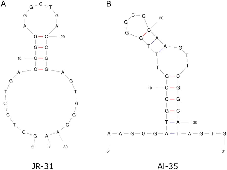 | ||
| Fig. 1 Secondary structures of the JR-31 (A) and AL-35 (B) aptamers. | ||
While the AL-35 aptamer is effective in many applications,25,26 its performance on the CNT FET didn't approach its performance in other sensing platforms. In the original paper from Alsager, the reported limit of detection is 200 pM,22 while Zheng reports a limit of detection more than 2 orders of magnitude higher of 50 nM.21 There isn't always a strong correlation between traditional measures of aptamer performance, such as Kd, and performance on a given sensing platform. For instance, the performance on a FET based sensor is strongly affected by the geometry of the structural shift upon target binding; if the aptamer binds strongly to a target but doesn't change shape in a way that moves the charged phosphate backbone closer to or farther away from the FET there will be no gating effect and thus no transduced signal. The conditions used for selecting and characterising the aptamer may also differ from sensing conditions. While this is often overlooked in aptasensor design, changes in the solution such as pH and ionic strength can have considerable impacts on binding affinity.27–29 Because of this it's difficult to predict aptamer performance in a given application, and it becomes necessary to compare aptamers directly on the same platform to determine which has preferable properties.
Here we test the AL-35 and JR-31 aptamers on the CNT FET sensing platform to determine which has preferable characteristics for this application. We show that both aptamers reliably produce a significant sensing signal on the CNT FET platform only at an E2 concentration of 1.0 μM, which is significantly higher than would be predicted from published values of Kd,22–24 which are in the order of 10 nM, and considerably higher than the 50 nM detection by Zheng using the AL-35 aptamer on a different CNT platform.21 The AL-35 aptamer produces a larger response to 1.0 μM E2 than the JR-31 while also giving in significantly noisier signals, with AL-35 aptasensors giving a normalised response of (8.1 ± 3.2) × 10−3, while JR-31 aptasensors gave a normalised response of (4.3 ± 2.2) × 10−3. In some cases the AL-35 aptamer produces a response at a lower E2 concentration of 110 nM, but this is not consistent across devices. JR-31 aptasensors display more consistent behaviour than AL-35 aptasensors, introducing the possibility that their signal to noise ratio could be improved considerably through more advanced analysis techniques.
The binding interactions of the aptamers with E2 were additionally characterized using circular dichroism (CD) spectroscopy. Binding can be inferred by observing the change in distortion of circularly polarized light (CPL) by the aptamer in the presence and absence of E2. A change in the ellipticity of the CPL reflects a change in aptamer structure associated with ligand binding. In this way CD spectroscopy is dually advantageous as it indicates the binding interaction as well as the magnitude of structure switching.30 Where the AL-35 aptamer exhibited minimal structure switching in 0.05 × PBS, in 1 × PBS there is a marked shift in the CD spectra in the presence of E2. Contrastingly, a greater shift is observed for JR-31 in 0.05 × PBS with very little indication of structure switching in 1 × PBS.
2 Experimental methods
2.1 Materials and equipment
Aptamers were purchased from Integrated DNA Technologies. Aptamers used for sensing were purchased with a 5′ amino modifier (C6). For CD spectroscopy aptamers were purchased unmodified. The sequences used are shown in Table 1.1-Pyrenebutyric acid N-hydroxysuccinimide ester (PBASE), N-(3-dimethylaminopropyl)-N′-ethylcarbodiimide hydrochloride (EDC), and N-hydroxysuccinimide (NHS), oestradiol (E2), and phosphate buffered saline (PBS) tablets were purchased from Sigma Aldrich. All solvents (methanol, ethanol, isopropyl alcohol, acetone, and dimethyl sulfoxide (DMSO)) were purchased from various suppliers at HPLC purity. AZ 326 developer and AZ 1518 photoresist were purchased from MicroChemicals. Polydimethylsiloxane (PDMS) is made from the SYLGARD 184 silicone elastomer kit according to package instructions. Carbon nanotubes were purchased from NanoIntegris as a 1 mg/100 mL solution of 90% semiconducting nanotubes. Poly-L-lysine was purchased from Sigma Aldrich as a 0.1% w/v solution in water. P doped Si wafers with a 300 nm SiO2 thermal growth were purchased from WaferPro. Chrome was purchased from Kurt J. Lesker as chrome plated tungsten rods. Gold was purchased as 99.99% pure wire from Regal Castings.
Ultrapure water is produced by a Milli-Q Synergy-UV system. Plasma cleaning and descum were performed in a Plasma Etch PE-50. Reactive ion etching was performed in an Oxford Instruments PlasmaLab 80 Plus. Thermal evaporation was performed in an Angstrom Engineering NexDep200. Photolithography was performed with a Karl Suss MJB3. Sensing experiments were performed with a NI PXIe system equipped with two PXIe-4138 source measure units and a PXIe-2737 matrix switch. Atomic force microscopy (AFM) was performed with a Nanosurf NaioAFM. CD spectroscopy was performed with an Applied Photophysics Chirascan-plus, using a 2 mm quartz cuvette supplied by Hellma Analytical.
The solutions used for sensing and CD spectroscopy measurements were prepared by dissolving PBS tablets in ultrapure water, to a 1× concentration of 137 mM NaCl, 2.7 mM KCl and 10 mM phosphate buffer, with a pH of 7.4. The 0.05 × PBS solution was made by diluting further with ultrapure water to 6.85 mM NaCl, 0.135 mM KCl and 0.5 mM phosphate.
DNA secondary structures were predicted using Mfold.31
2.2 Truncation of the Jauset-Rubio aptamer
Jauset-Rubio et al. presented 3 oestradiol aptamers, referred to in their paper as E11, E26, and E28.23 An analysis of both primary and secondary structure, seen in Fig. 2, shows that all three aptamers share a 21-mer sequence, with one mer difference in E28, which indicates that this sequence and its associated secondary structure is the binding site for oestradiol. As E28 had favourable performance in Jauset-Rubio's work, a 31-mer truncation of E28 was made, including the 21-mer shared sequence, 6 additional mers on the 5′ end, and 4 additional mers on the 3′ end.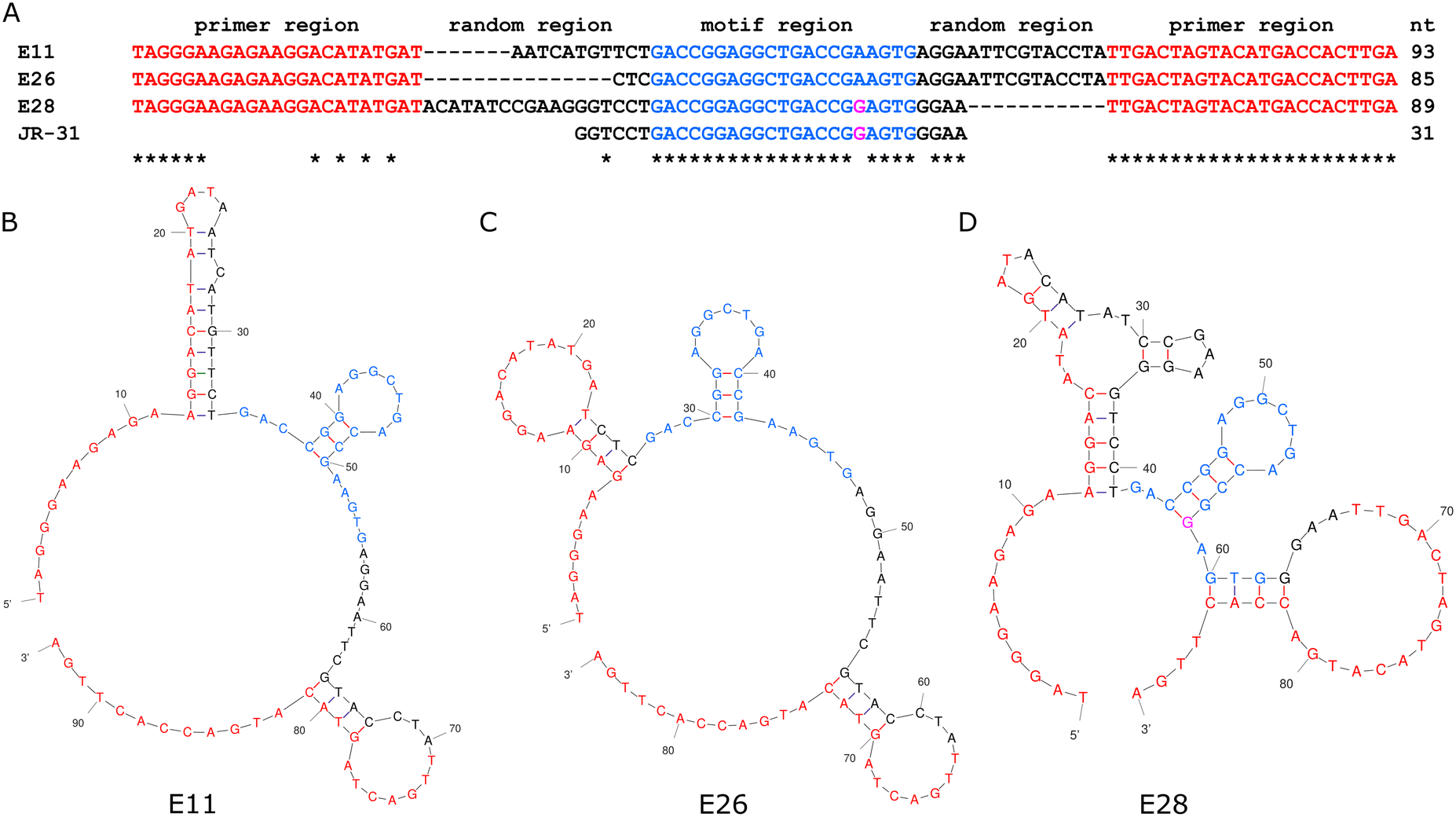 | ||
| Fig. 2 The primary (A) and secondary structures of the E11 (B), E26 (C), and E28 (D) aptamers from Jauset-Rubio et al., highlighted to show the motif on which the JR-31 aptamer is based. | ||
2.3 Sensor fabrication
Carbon nanotube network field effect transistors (CNT FETs) were fabricated on a Si/SiO2 substrate in four steps, depicted in Fig. 3, three of which use the same photolithography process for patterning. Once the CNT FETs were fabricated they were functionalised with aptamer using PBASE as a linker.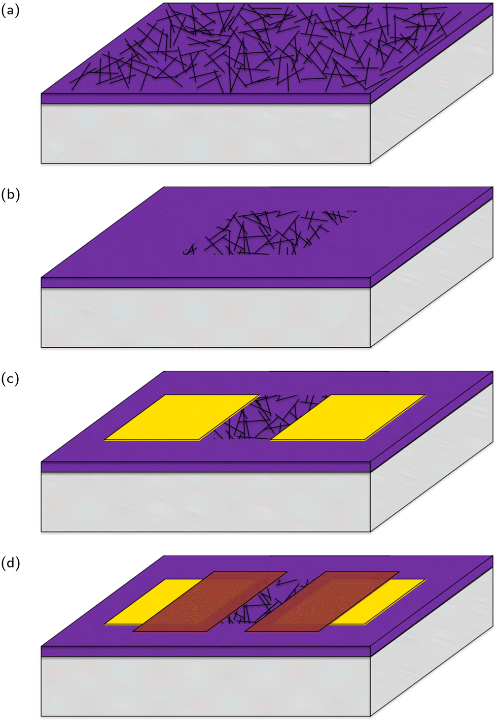 | ||
| Fig. 3 A stylised depiction of the fabrication process. (a) CNT deposition, (b) reactive ion etching, (c) electrode deposition, (d) encapsulation. | ||
![[thin space (1/6-em)]](https://www.rsc.org/images/entities/char_2009.gif) :1 ratio for 35 s, and is then submerged in ultrapure water, rinsed in clean ultrapure water, and dried in N2. In the case of electrodes and encapsulation, the wafer is then exposed to oxygen plasma (PE-50, 50 W, 350 mTorr) for 2 s as a descum step.
:1 ratio for 35 s, and is then submerged in ultrapure water, rinsed in clean ultrapure water, and dried in N2. In the case of electrodes and encapsulation, the wafer is then exposed to oxygen plasma (PE-50, 50 W, 350 mTorr) for 2 s as a descum step.
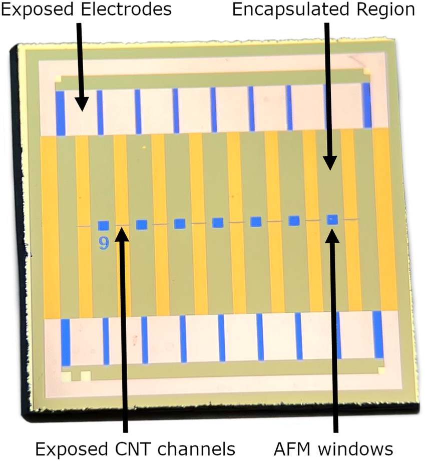 | ||
| Fig. 4 A photo of a completed chip. For scale, the chip is 12 mm by 12 mm. | ||
2.4 Circular dichroism spectroscopy
CD spectroscopy was recorded between 200 and 320 nm in a 2 mm quartz cuvette at 20 °C. Spectra were averaged from three scans, which were recorded at a bandwidth of 2 nm, a step size of 2 nm and a 1 s time per point. The final spectra were normalized by zeroing the ellipticity at 320 nm. All samples were prepared in 0.05 × or 1 × PBS depending on the ionic conditions, and 5% EtOH. The final concentration of the aptamer was 5 μM and the final concentration of the E2 was 1× or 5× the molar concentration of aptamer, 5 μM and 25 μM respectively. The aptamer samples were heated to 95 °C for 5 min and cooled rapidly in an ice-water bath for 10 minutes to ensure intramolecular folding. A ‘no-cell’ background spectra was acquired and automatically subtracted from all measurements. The CD spectra of no target buffer and buffer containing 0×, 1×, and 5× oestradiol were acquired as blank measurements. These blank measurements were subtracted from the acquired aptamer and aptamer with target measurements. These blank spectra can be found in the ESI,†Fig. 1. No smoothing was applied to the acquired spectra.2.5 Sensing
Oestradiol (E2) is stored at −20 °C in ethanol, at concentrations of 20 nM, 200 nM, 2 μM, 20 μM and 200 μM. 20 μL volumes of each concentration are placed into glass vials, along with 380 μL of 0.05 × PBS to give final concentrations of 1 nM, 10 nM, 100 nM, 1 μM and 10 μM in a 5% ethanol solution. These solutions are vortex mixed for 30 s at 3000 RPM, both upon making them and immediately prior to using them. Glass and PTFE tools and containers are used when handling E2 containing solutions to prevent adsorption and the resulting drop in E2 concentration in solution.32 Aqueous E2 solutions are made and used on the same day.Wells are made from PDMS and are cleaned with ethanol and dried thoroughly before being pressed onto the chips. A Ag/AgCl reference electrode is suspended in the well to provide liquid gating. 100 μL of 0.05 × PBS, 5% ethanol solution is added to the well. A further 120 μL is added and then removed to ensure that the reference electrode is properly wetted by the sensing solution. A gate voltage of 0 V and a drain source voltage of 100 mV are applied to the device. To measure all 8 sensors in the same sensing experiment, the drain and source connections are routed through a switch matrix, which switches between transistors at approximately 230 ms intervals. Every 300 s a 20 μL addition of solution is made. The first addition contains no analyte. Subsequent additions contain, in order, 1 nM, 10 nM, 100 nM, 1 μM, and 10 μM of E2, which correspond to concentrations in the well of 140 pM, 1.4 nM, 12 nM, 110 nM, and 1.0 μM.
3 Results
3.1 Circular dichroism spectroscopy
The circular dichroism spectra, seen in Fig. 5, for both the AL-35 and JR-31 aptamers in both ionic conditions consist of a positive band in the 260 to 280 nm range, a negative band near 245 nm and another positive band near 220 nm, which is characteristic of a B-form DNA structure.33 This is consistent with the predicted helix–bulge–hairpin-loop and hairpin-loop structures of AL-35 and JR-31 respectively. Further, the CD-spectra observed for the AL-35 aptamer is consistent with the structure determined from molecular dynamics simulations by Hilder and Hodgkiss,34 and Eisold and Labudde35 for the 22-mer and 35-mer variants respectively.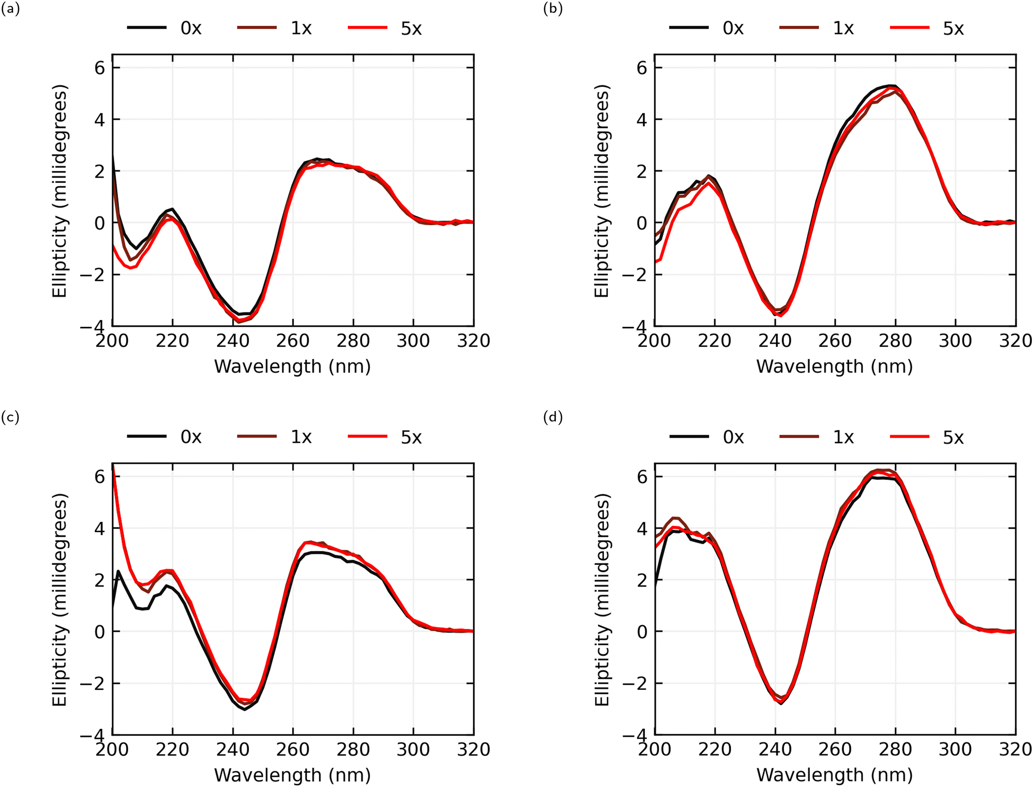 | ||
| Fig. 5 Circular dichroism spectra of AL-35 and JR-31 aptamers with E2 concentrations at 0× (black), 1× (red-brown), and 5× (red) the aptamer concentration. (a) AL-35 in 0.05 × PBS, 5% EtOH, (b) JR-31 in 0.05 × PBS, 5% EtOH, (c) AL-35 in 1 × PBS, 5% EtOH, (d) JR-31 in 1 × PBS, 5% EtOH. | ||
In the 0.05 × PBS condition for the AL-35 aptamer only a minor shift in the tertiary structure range (>250 nm) is observed in the 260–270 nm range, with an average shift in this range of −0.112 millidegrees for 1× oestradiol, and −0.242 millidegrees for 5× oestradiol. In the secondary structure range (<250 nm) greater changes are observed, with shifts of −0.329 millidegrees and −0.394 millidegrees at the 220 nm peak for 1× and 5× oestradiol respectively. While this indicates that E2-binding is occurring; either the final structure of the binding pocket is largely formed in low-ionic conditions, or the binding interaction is diminished due to unsatisfied ion dependence. In the 1 × PBS condition there is a greater shift in the CD spectra in both the tertiary structure range (averaging 0.396 millidegrees and 0.335 millidegrees across the 260–270 nm band for 1× and 5× oestradiol concentrations respectively) and secondary structure range (0.558 millidegrees and 0.680 millidegrees for 1× and 5× respectively at 220 nm) in response to the addition of E2 and the resultant binding. There appears to be little change between 1× and 5× oestradiol concentrations, suggesting that the majority of the aptamers are bound to oestradiol at a 1× concentration.
In the 0.05 × PBS condition the JR-31 aptamer shows a greater CD shift in the tertiary structure compared to the AL-35 aptamer across a wider range of wavelengths, with an average shift in the 260–280 nm range of −0.443 millidegrees for 1× oestradiol concentration and −0.252 millidegrees for a 5× concentration. A shift is also observed in the secondary structure range (−0.143 and −0.378 millidegrees for 1× and 5× respectively at 220 nm). In the 1 × PBS condition only minor tertiary and secondary structure changes are observed, averaging 0.311 and 0.204 millidegrees across 260–280 nm for 1× and 5× oestradiol concentrations respectively, and 0.250 and 0.085 millidegrees at 220 nm. This indicates that the binding pocket is predominantly preformed in higher ionic conditions. The JR-31 aptamer generally shows smaller shifts in ellipticity at 5× concentrations of oestradiol than at 1× concentrations. This suggests that the aptamer is saturated at a 1× concentration, and that an excess of oestradiol might interfere with the binding interaction.
3.2 FET characterisation
After functionalisation the FETs are characterised with atomic force microscopy (AFM) to observe the network morphology, and a gate voltage sweep to determine the electrical characteristics. Fig. 6 shows an AFM image of a typical CNT network film where there are dense and uniform layers of CNTs observed. These CNT networks are made from a liquid CNT dispersion, where limited CNT bundling is expected. However, with heights on the order of 9 nm above the background in places, we can see that multiple CNTs have stacked on top of each other. These CNT networks are of good quality with a known semiconducting content of 90% as listed from the manufacturer.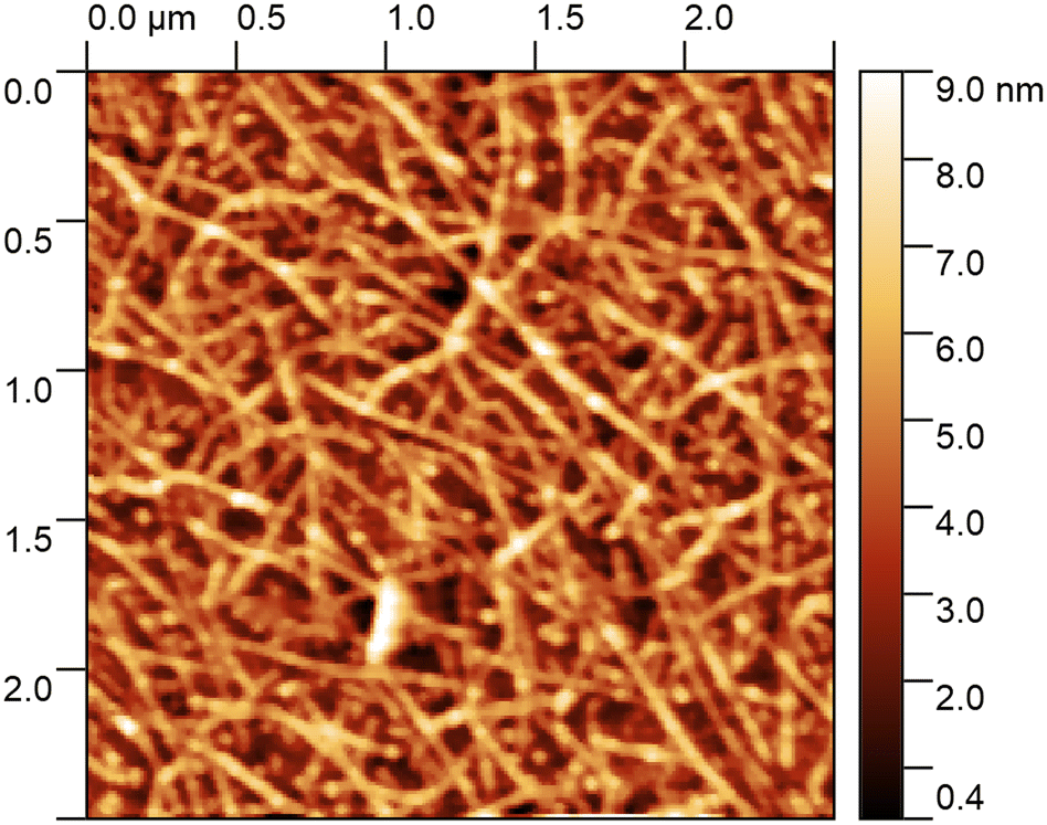 | ||
| Fig. 6 An AFM scan of the CNT network on one of the chips presented here, showing a dense and uniform network with minimal bundling of CNTs. | ||
Gate voltage sweeps show ambipolar devices, with hole conduction dominating at the gate voltages used in sensing experiments. On currents are typically in the order of 100 nA to 1 μA, and on off ratios range from 103 to 104. An example gate sweep is shown in Fig. 7 and the full set of gate sweeps can be found in the ESI,†Fig. 3–5.
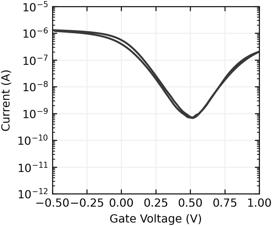 | ||
| Fig. 7 A gate transfer sweep of a CNT FET aptasensor. VDS = 100 mV. | ||
3.3 Sensing
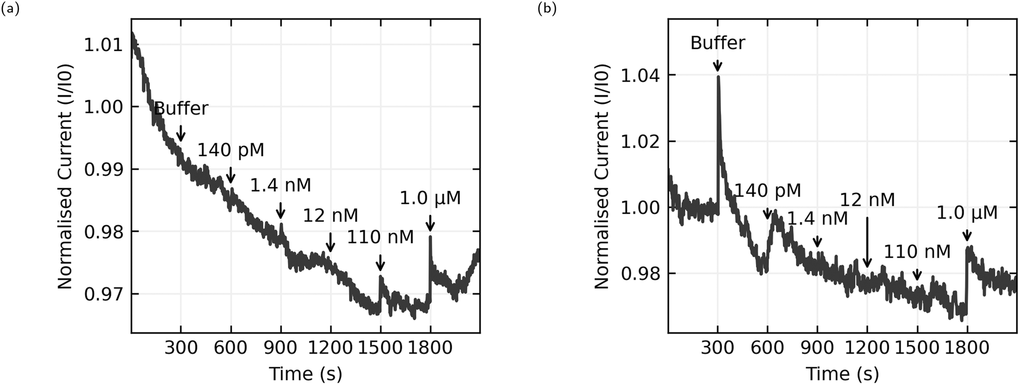
The data presented here comes from 6 chips with 8 sensors per chip. 3 chips were functionalised with AL-35 aptamer, with a final yield of 11 working sensors of a possible 24, while the other 3 were functionalised with JR-31 aptamer with a final yield of 8 working sensors from a possible 24. This is a low yield of working sensors (46% and 33% respectively), suggesting an issue with the functionalisation process that will be discussed later. Fig. 8 shows the normalised current as a function of time for 4 typical sensors, with the time and concentration of each addition of analyte solution annotated on the graph. Plots (a) and (b) are AL-35 aptasensors, while (c) and (d) are JR-31 aptasensors. Normalised current against time plots for all sensors can be found in the ESI† in Fig. 6–8.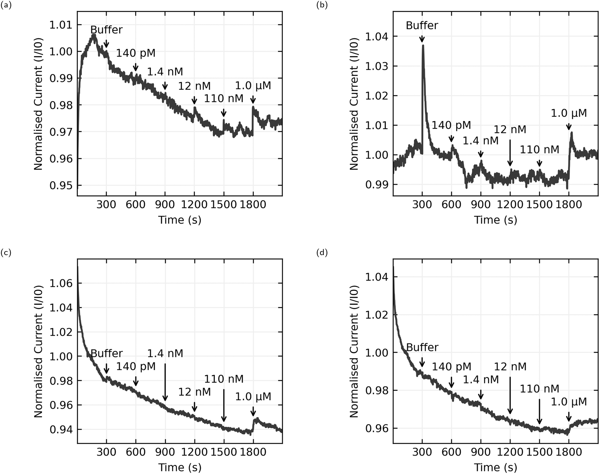 | ||
| Fig. 8 Normalised current against time plots, with annotations indicating the time of each addition and the E2 concentration in the well after the addition. (a) and (b) are from sensors functionalised with AL-35 aptamer, (c) and (d) are functionalised with truncated JR-31 aptamer. | ||
All sensors included in this study have a notable increase in current when the concentration of E2 in the well reaches 1.0 μM. The qualitative behaviour of the sensors is dependant on the aptamer they're functionalised with. The JR-31 aptasensors are more predictable, with all devices showing a large transient on the onset of sensing that decays to a steady downwards drift, and a positive step when the E2 concentration reaches 1.0 μM. The AL-35 aptasensors are generally less predictable. The sensor depicted in Fig. 8(a) has a large transient on the onset of sensing in the opposite direction to the JR-31 aptasensors. This transient decays away to a downwards drift, and in addition to the positive step at 1.0 μM there is a smaller step at 110 nM addition. By contrast, the other AL-35 aptasensor seen in (b) has a much smaller initial transient, a less pronounced drift after the initial transient, a large spike that appears to decay away completely upon the addition of buffer, much higher low frequency noise, and no apparent step at the 110 nM addition. The physical mechanism governing the differences in drift between the two aptamers is not yet fully understood. However, we do note that the JR-31 aptasensors all display a consistent drift behaviour of reducing current with time, which is different to the AL-35 aptasensors.
To quantitatively analyse and compare the data the normalised current signals were then processed to calculate the change in normalised current upon making an addition of analyte. The data are first passed through a median filter with a 40 second window to remove brief spikes and reduce the effect of high frequency noise while preserving steps.36 To calculate the step size, we take the average over 120 second windows before and after the addition is made, excluding 15 seconds either side of this time to account for inaccuracies in the addition time, and report the difference between these averages. It should be noted that drift in the signal will skew the results, with the downward drift seen in many of the sensors presented here causing a negative shift in measured step size. The results for each individual sensor can be found in the ESI,†Fig. 9–11. These values are then aggregated by grouping the sensors by receptor and calculating the mean and standard deviation of the response to each concentration of analyte.
 | ||
| Fig. 9 Average and standard deviation of the size of the step in current upon the addition of analyte against analyte concentration. (a) Shows the results from AL-35 aptasensors, while (b) shows JR-31 aptasensors. | ||
 | ||
| Fig. 10 Sensing results from two AL-35 aptasensors. (a) Shows a step at 110 nM while (b) does not. | ||
 | ||
| Fig. 11 A transistor under an optical microscope before (a) and after (b) being immersed in PBASE in DMSO solution. The slightly tinted strip through the middle of the device is the CNT network. The encapsulation layer has been damaged in the area where it is in contact with the CNTs. | ||
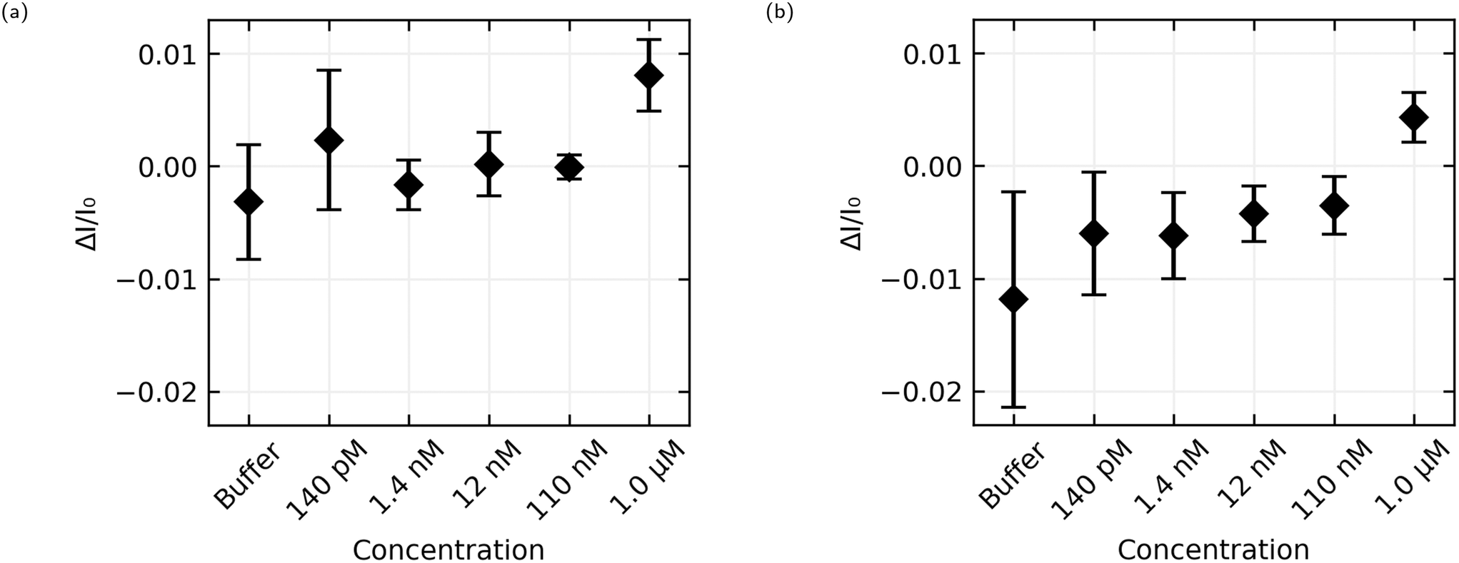
The aggregated sensing results for both aptamers are shown in Fig. 9, and in numerical form in Table 2. While some of the individual sensing results with AL-35 aptasensors appear to demonstrate a step at a concentration of 110 nM E2, the mean step size of (−0.1 ± 1.1) × 10−3 for this addition shows that this response cannot be reliably distinguished from a non response using the analysis methods presented here. At a concentration of 1.0 μM the greater signal from the AL-35 aptasensors appears to outweigh the higher spread in responses, with a mean step of (8.1 ± 3.2) × 10−3 putting this response 2.5 standard deviations above zero, to the JR-31 aptasensors' response of (4.3 ± 2.2) × 10−3, 2.0 standard deviations above zero.
| 0 M | 140 pM | 1.4 nM | 12 nM | 110 nM | 1.0 μM | |
|---|---|---|---|---|---|---|
| AL-35 aptasensors | −3.2 ± 5.1 | 2.3 ± 6.2 | −1.7 ± 22 | 0.2 ± 2.8 | −0.1 ± 1.1 | 8.1 ± 3.2 |
| JR-31 aptasensors | −11.9 ± 9.6 | −6.0 ± 5.5 | −6.2 ± 3.8 | −4.3 ± 2.5 | −3.5 ± 2.6 | 4.3 ± 2.2 |
The AL-35 aptasensors show a higher signal relative to the spread in their responses. While this might suggest that the AL-35 aptamer is superior in this application, the predictability of the results from JR-31 aptasensors may allow for more advanced analysis techniques to compensate for this gap. As seen in Fig. 8(c) and (d), JR-31 aptasensors have a consistent and smooth downwards drift with slight positive curvature, which results in a negative offset in calculated step size. This can be seen in the average responses in Fig. 9(b), where the additions from 140 pM to 110 nM have a negative offset that is becoming slightly more positive with subsequent additions, excepting a slight dip at 12 nM. If we accept the qualitative result that there is no response to any E2 concentration below 1.0 μM, and that these negative values are the result of drift, we can linearly extrapolate these values to get an approximation of the expected step size if there was no response to 1.0 μM E2. In making this extrapolation we exclude the response to buffer, as this is skewed downward by the sharp initial transient seen in Fig. 8(c) and (d), and find that the expected value is −2.7 × 10⁻³. This places the JR-31 aptasensors average step response to 1.0 μM E2 at 3.2 standard deviations above the expected value if there was no response, which is slightly better than the AL-35 aptasensors. This analysis method is crude, but it demonstrates that the performance of JR-31 aptasensors could exceed AL-35 aptasensors if more advanced analysis is used. Conversely, the unpredictable behaviour of the AL-35 aptasensors makes more advanced analysis less promising.
4 Discussion
4.1 Comparison with Zheng
The most natural point of comparison in this work is with Zheng 2015,21 the first report of successful sensing of E2 with a CNT aptasensor. Zheng uses the AL-35 aptamer and reports a limit of detection of 50 nM, more than an order of magnitude lower than the 1.0 μM limit from this work.When considering the difference in limit of detection its best to look at the response when the concentration in the well reaches 110 nM. While this cannot consistently be distinguished from noise across the whole set of sensors, some sensors do appear to have a response to this addition. For instance, Fig. 10(a) shows a sensor with a small but distinct step at 110 nM, whereas Fig. 10(b) shows no step at 110 nM. Despite efforts to improve the consistency of the fabrication process, random CNT networks are stochastic by nature, and the functionalisation process is sensitive in ways that will be discussed later. The resulting sensors aren't exactly the same. Some sensors are unusually bad, and these were excluded from this data set for not displaying any clear response at 1.0 μM, and some sensors are unusually good. If we accept that an unusually good device is producing a real sensing response, it follows that the responses to 110 nM E2 concentrations depicted in Fig. 8(a) and 10(a) can be genuine, even if many other sensors in the same data set don't produce a response and the aggregated responses aren't distinguishable from a non response. This means that the discrepancy in limit of detection between this work and the work of Zheng et al. is much lower, 110 nM here versus 50 nM in Zheng's work, and could be attributed to different selection of analyte concentrations rather than a genuine difference in sensor performance.
The primary difference between the sensor platform used in this work and the work published by Zheng et al. is the method of depositing the CNT network. In Zheng's work CNTs are purchased in a bulk solid form referred to as bucky paper. Si/SiO2 wafers are functionalised with 2-mercaptopyridine. The CNTs are dispersed in 1,2-dichlorobenzene, and the wafers are immersed in the CNT solution. This method of deposition results in a high degree of bundling of CNTs, i.e. there are usually multiple CNTs stuck together that are running in parallel. By contrast the aqueous deposition process used in this work results in less bundling of the CNTs, with each nanotube being separated from the others. The aqueous deposition process produces more consistent networks, and so there is less variability in transistor characteristics. However, these networks are typically of a higher density, and there is literature to suggest that lower density networks, just above the percolation threshold, have higher sensitivity when used as sensors.11
4.2 Sensor yield
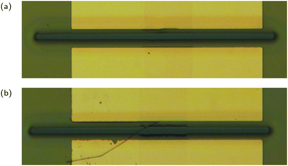
Of the 48 transistors functionalised for use as sensors in this work, only a total of 19, or 40%, were able to detect E2. This excludes transistors from other fabrication batches where none of the transistors could detect E2. Apart from limiting both the statistical analysis that can be done on these devices and iterative improvements to the sensing protocol, this raises concerns about the fabrication and functionalisation process. The most likely culprit for this low yield is the functionalisation process, specifically the PBASE step. Prior to functionalising the transistors there is generally a yield of approximately 90%, with good devices being defined as having an on current greater than 50 nA and an on off ratio greater than 100. Poor devices typically occur near the edge of the wafer where damage from handling during the fabrication process is more likely. Post functionalisation the devices fall into one of three categories: working sensors, that is devices that display a response to analyte; failed sensors, any device that continues to operate as a transistor but fails to respond to analyte; and failed transistors, any device that has its on current drop below 50 nA (typically these devices drop below 100 pA, the accuracy limit of the measurement system). It is noteworthy that the devices that do work as sensors show relatively consistent performance, particularly the JR-31 sensors where the drift behaviour is more predictable.The most likely explanation for failed transistors is solvent wicking along CNTs and degrading the electrical connection between the CNT network and the chrome/gold electrodes. Fig. 11 shows a transistor under an optical microscope, before and after the chip was functionalised with PBASE in DMSO solution. The encapsulation layer can be seen peeling away in the region where it connects to the carbon nanotube network. A complete solution to this problem has yet to be developed, however the use of titanium as opposed to chrome in the electrode deposition process and the use of SU8 photoresist as opposed to AZ 1518 in the encapsulation layer are promising solutions. This likely was not an issue for past work using CNT network FETs as aptasensors for two reasons. First, past work used a CNT deposition process that resulted in highly bundled CNT networks. These networks have a much greater height on the surface of the wafer than the unbundled networks produced with the aqueous deposition process used in this work, and so have much more area to connect with the electrode. These devices were also functionalised with a PBASE in methanol solution. The use of methanol has the advantage of being less destructive to the encapsulation layer, however the solubility of PBASE in methanol is much lower than in DMSO. Various techniques including heating and ultrasonication can assist with dissolving PBASE in methanol, but these techniques introduce more intensive handling to the most sensitive part of the CNT aptasensor fabrication process, functionalisation.
The devices that continued to work as transistors but did not give a sensing response call into question the reliability of the functionalisation process. The inclusion of EDC/NHS in the aptamer solution is intended to mitigate one potential failure point in this process, hydrolysis of the PBASE into 1-pyrenebutyric acid. All sensors in this work had EDC/NHS included in this step, and each chip included had at least one working sensor. Other devices that were made using the same procedure without EDC/NHS were excluded as none of them produced a sensing response. This suggests that hydrolysis may be contributing to the low yield of devices, however further investigation is required to confirm this and to identify any other factors that may be contributing.
An important distinction between the sensors presented in this work and Zheng's work is the use of a multiplexed measurement system. Zhengs work uses chips with four transistors per chip, but only measures one transistor during sensing. This transistor is selected based on pre-sensing, post-functionalisation measurements and so maximises the chances that the sensor measured will be a working sensor. By contrast, the chips in this work have eight transistors and all are measured simultaneously during sensing. Prior to this work is was not known whether the transistors that aren't being measured would have functioned as sensors.
4.3 Discrepancy between Kd and limit of detection in sensing
The AL-35 aptamer has a dissociation constant, Kd, reported in the literature between 14 nM and 23 nM.22,24 Given that the Kd corresponds to the E2 concentration in which half the aptamers are bound to E2, this would suggest a limit of detection for the sensors that is significantly less than 10 nM. Indeed Alsager et al. report a 200 pM limit of detection using a gold nanoparticle colourimetric sensor.22 Other reports using the same aptamer or a different truncation of the same sequence have limits of detection of 5 nM, 50 nM, and 1 fM using the size contraction of aptamer functionalised nanoparticles, lateral flow assays, and electrochemical sensors respectively.25,26,37 The aptasensors we present using AL-35 aptamers only reliably detect E2 when the concentration in the well reaches 1.0 μM, at least 2 orders of magnitude higher than would be predicted based on published Kd values. While FET sensors offer many advantages for point of care tests, particularly low cost for mass production and the ease of automating analysis of an all-electronic sensor, the higher limit of detection needs to be understood and addressed in order to make them a viable alternative to other sensing platforms.8Our CD spectroscopy results suggest the ionic strength of the sensing buffer as an explanation for this discrepancy. The structure shift seen in the AL-35 aptamer in 0.05 × PBS is considerably smaller than the shift seen in 1 × PBS. While this would suggest that 1 × PBS is the preferable sensing environment, the increased ionic screening caused by higher ionic strengths is well known to result in a reduced signal in FET biosensors.38,39 This dilemma can potentially be addressed through the use of sensing methods or sensor modifications that mitigate the effect of ionic screening,39–41 however it is also possible to create aptamers that produce sensing signals in high ionic strength solutions without unusual modifications to the sensor or sensing protocol.42,43 Producing aptamers using the capture-SELEX method, which selects for structure switching aptamers, would benefit sensor applications.44
Our results suggest that aptamers the haven't been designed for a specific application, such as FET biosensors, are unlikely to perform as well as their published characteristics would suggest. Where possible there should be close collaboration between researchers who are designing aptamers and researchers designing sensors to ensure compatibility between platform and aptamer. Where this isn't possible, we encourage a greater consideration of the SELEX conditions when choosing an aptamer for use with a given sensing platform. Additionally, implementing methods intended to mitigate ionic screening and allow for sensing in higher ionic strengths may widen the range of aptamers that can be used for FET sensors.
4.4 Differences in sensor behaviour based on aptamer
Examining both the raw and aggregated data makes it clear that the AL-35 aptasensors and the JR-31 aptasensors show considerably different drift in drain current, even when the oestradiol concentration is below the limit of detection. The cause of this difference in behaviour requires more investigation in order to be properly understood. Although there are molecular dynamics simulations for the AL-35 aptamer,35 there are no comparable simulations for the JR-31 aptamer. The AL-35 simulations are not constrained by either nuclear magnetic resonance (NMR) data or isothermal titration calorimetry (ITC) data. Structural characterisation, particularly with NMR, will allow for more accurate modelling, and thus will offer an improved understanding of the differences in sensor behaviour.45 This characterisation may be challenging due to the low solubility of oestradiol, which we observed to be approximately 30 μM in 5% EtOH solution.Regardless as to the cause, the current drift behaviour of the JR-31 aptasensors has been consistent across many devices, a repetition that may make those devices more amenable to advanced signal processing techniques for oestradiol detection at concentrations above 1 μM.
5 Conclusions
We present CNT FET aptasensors functionalised with two different oestradiol aptamers, AL-35 and the JR-31. Both aptamers produced working sensors with a similar limit of detection of 1.0 μM. The JR-31 functionalised sensors had more consistent behaviour, suggesting that these devices may be easier to develop mathematical models for, allowing for more accurate and reliable numerical analysis. The AL-35 functionalised sensors displayed less consistent behaviour, but some individual sensors had a lower limit of detection of 110 nM despite the group as a whole only reliably detecting at 1.0 μM. This comparison shows that the choice of aptamer can in some circumstances make a qualitative difference to sensor behaviour, even below the limit of detection.The results from CD spectroscopy suggest that the reason our observed limit of detection is much higher than would be expected from published values for Kd is the difference between the ionic environment used for SELEX and characterising the aptamers, and the environment used for sensing. The competing requirements of the platform, namely low ionic strength to reduce ionic screening, and the aptamers, which require higher ionic strength for optimal binding, show that more coordinated work is required on both the platform and the receptor to realise effective FET biosensors.
With regard to the platform, a better understanding of the process of functionalising CNTs with aptamers will allow for more consistent and higher performance of these sensors. The CNT network itself has the potential for significant further optimisation as CNT deposition processes develop.11
Author contributions
Conceptualisation: Erica Cassie, Natalie O. V. Plank. Data curation: Erica Cassie, Hamish Dunham. Formal analysis: Erica Cassie, Hamish Dunham. Funding acquisition: Natalie O. V. Plank. Investigation: Erica Cassie, Hamish Dunham. Methodology: Erica Cassie, Hamish Dunham, Erica Happe, Hong Phan T. Nguyen, Natalie O. V. Plank. Supervision: Natalie O. V. Plank, Janet L. Pitman. Writing – original draft: Erica Cassie, Hamish Dunham, Natalie O. V. Plank. Writing – review and editing: Erica Cassie, Hamish Dunham, Natalie O. V. Plank.Conflicts of interest
There are no conflicts to declare.Acknowledgements
This work was supported by the Marsden Fund Council from Government funding (New Zealand), managed by Royal Society Te Apārangi, grant number VUW1708. EC would like to thank Matire Ward for her assistance in developing protocols for handling and diluting steroids.Notes and references
- L. Syedmoradi, M. Daneshpour, M. Alvandipour, F. A. Gomez, H. Hajghassem and K. Omidfar, Biosens. Bioelectron., 2017, 87, 373–387 CrossRef CAS PubMed.
- C. S. Kosack, A. L. Page and P. R. Klatser, Bull. W. H. O., 2017, 95, 639–645 CrossRef PubMed.
- S. Kahyaoglu, O. H. Yumusak, A. S. Ozgu-Erdinc, S. Yilmaz, I. Kahyaoglu, Y. Engin-Ustun and N. Yilmaz, Syst. Biol. Reprod. Med., 2015, 61, 233–237 CrossRef CAS PubMed.
- E. B. C. T. C. Group, Lancet, 2005, 365, 1687–1717 CrossRef PubMed.
- K. Maehashi, T. Katsura, K. Kerman, Y. Takamura, K. Matsumoto and E. Tamiya, Anal. Chem., 2007, 79, 782–787 CrossRef CAS PubMed.
- C. Wang, X. Cui, Y. Li, H. Li, L. Huang, J. Bi, J. Luo, L. Q. Ma, W. Zhou, Y. Cao, B. Wang and F. Miao, Sci. Rep., 2016, 6, 1–8 CrossRef PubMed.
- F. Khosravi, S. M. Loeian and B. Panchapakesan, Biosensors, 2017, 7, 17 CrossRef PubMed.
- K. Ryu, C. Wang, J. Zhang, L. G. D. Arco, A. Badmaev and C. Zhou, Nano Lett., 2009, 9, 4285–4291 CrossRef PubMed.
- T. Durkop, S. A. Getty, E. Cobas and M. S. Fuhrer, Nano Lett., 2004, 4, 35–39 CrossRef.
- E. S. Snow, J. P. Novak, P. M. Campbell and D. Park, Appl. Phys. Lett., 2003, 82, 2145–2147 CrossRef CAS.
- M. Thanihaichelvan, L. A. Browning, M. P. Dierkes, R. M. Reyes, A. V. Kralicek, C. Carraher, C. A. Marlow and N. O. Plank, Biosens. Bioelectron., 2019, 130, 408–413 CrossRef CAS PubMed.
- M. A. Topinka, M. W. Rowell, D. Goldhaber-Gordon, M. D. McGehee, D. S. Hecht and G. Gruner, Nano Lett., 2009, 9, 1866–1871 CrossRef CAS PubMed.
- A. Kim, C. S. Ah, C. W. Park, J. H. Yang, T. Kim, C. G. Ahn, S. H. Park and G. Y. Sung, Biosens. Bioelectron., 2010, 25, 1767–1773 CrossRef CAS PubMed.
- T. Ono, Y. Kanai, K. Inoue, Y. Watanabe, S. I. Nakakita, T. Kawahara, Y. Suzuki and K. Matsumoto, Nano Lett., 2019, 19, 4004–4009 CrossRef CAS PubMed.
- T. Murugathas, H. Y. Zheng, D. Colbert, A. V. Kralicek, C. Carraher and N. O. Plank, ACS Appl. Mater. Interfaces, 2019, 11, 9530–9538 CrossRef CAS PubMed.
- S. Song, L. Wang, J. Li, C. Fan and J. Zhao, TrAC, Trends Anal. Chem., 2008, 27, 108–117 CrossRef CAS.
- C. Tuerk and L. Gold, Science, 1990, 249, 505–510 CrossRef CAS PubMed.
- A. D. Ellington and J. W. Szostak, Nature, 1990, 346, 818–822 CrossRef CAS PubMed.
- I. Heller, A. M. Janssens, J. Mannik, E. D. Minot, S. G. Lemay and C. Dekker, Nano Lett., 2007, 8, 591–595 CrossRef PubMed.
- H. Y. Zheng, O. A. Alsager, B. Zhu, J. Travas-Sejdic, J. M. Hodgkiss and N. O. V. Plank, Nanoscale, 2016, 8, 13659–13668 RSC.
- H. Y. Zheng, O. A. Alsager, C. S. Wood, J. M. Hodgkiss and N. O. V. Plank, J. Vac. Sci. Technol., B: Nanotechnol. Microelectron.: Mater., Process., Meas., Phenom., 2015, 33, 06F904 Search PubMed.
- O. A. Alsager, S. Kumar, B. Zhu, J. Travas-Sejdic, K. P. McNatty and J. M. Hodgkiss, Anal. Chem., 2015, 87, 4201–4209 CrossRef CAS PubMed.
- M. Jauset-Rubio, M. L. Botero, V. Skouridou, G. B. Aktas, M. Svobodova, A. S. Bashammakh, M. S. El-Shahawi, A. O. Alyoubi and C. K. O'Sullivan, ACS Omega, 2019, 4, 20188–20196 CrossRef CAS PubMed.
- M. Svobodova, V. Skouridou, M. L. Botero, M. Jauset-Rubio, T. Schubert, A. S. Bashammakh, M. S. El-Shahawi, A. O. Alyoubi and C. K. O'Sullivan, J. Steroid Biochem. Mol. Biol., 2017, 167, 14–22 CrossRef CAS PubMed.
- B. Zhu, O. A. Alsager, S. Kumar, J. M. Hodgkiss and J. Travas-Sejdic, Biosens. Bioelectron., 2015, 70, 398–403 CrossRef CAS PubMed.
- O. A. Alsager, S. Kumar and J. M. Hodgkiss, Anal. Chem., 2017, 89, 7416–7424 CrossRef CAS PubMed.
- G. R. Bishop, J. Ren, B. C. Polander, B. D. Jeanfreau, J. O. Trent and J. B. Chaires, Biophys. Chem., 2007, 126, 165–175 CrossRef CAS PubMed.
- P. H. Lin, S. J. Tong, S. R. Louis, Y. Chang and W. Y. Chen, Phys. Chem. Chem. Phys., 2009, 11, 9744–9750 RSC.
- M. A. Neves, S. Slavkovic, Z. R. Churcher and P. E. Johnson, Nucleic Acids Res., 2017, 45, 1041–1048 CAS.
- Y. Kerler, S. Sass, C. Hille and M. M. Menger, in Determination of Aptamer Structure Using Circular Dichroism Spectroscopy, ed. G. Mayer and M. M. Menger, Springer US, New York, NY, 2023, pp. 119–128 Search PubMed.
- M. Zuker, Nucleic Acids Res., 2003, 31, 3406–3415 CrossRef CAS PubMed.
- P. F. Bruning, K. M. Jonker and A. W. Boerema-Baan, J. Steroid Biochem., 1981, 14, 553–555 CrossRef CAS PubMed.
- J. Kypr, I. Kejnovská, D. Renčiuk and M. Vorlíčková, Nucleic Acids Res., 2009, 37, 1713–1725 CrossRef CAS PubMed.
- T. A. Hilder and J. M. Hodgkiss, ChemPhysChem, 2017, 18, 1881–1887 CrossRef CAS PubMed.
- A. Eisold and D. Labudde, Molecules, 2018, 23, 1690 CrossRef PubMed.
- J. W. Tukey, Exploratory Data Analysis, Addison-Wesley, 1977 Search PubMed.
- O. A. Alsager, S. Kumar, G. R. Willmott, K. P. McNatty and J. M. Hodgkiss, Biosens. Bioelectron., 2014, 57, 262–268 CrossRef CAS PubMed.
- H. M. So, K. Won, Y. H. Kim, B. K. Kim, B. H. Ryu, P. S. Na, H. Kim and J. O. Lee, J. Am. Chem. Soc., 2005, 127, 11906–11907 CrossRef CAS PubMed.
- N. Gao, W. Zhou, X. Jiang, G. Hong, T. M. Fu and C. M. Lieber, Nano Lett., 2015, 15, 2143–2148 CrossRef CAS PubMed.
- G. S. Kulkarni and Z. Zhong, Nano Lett., 2012, 12, 719–723 CrossRef CAS PubMed.
- C. S. Ah, A. Kim, W. J. Kim, C. W. Park, C. G. Ahn, J. H. Yang, B. Baek, T. Y. Kim and G. Y. Sung, Bull. Korean Chem. Soc., 2010, 31, 1561–1567 CrossRef CAS.
- N. Nakatsuka, K. A. Yang, J. M. Abendroth, K. M. Cheung, X. Xu, H. Yang, C. Zhao, B. Zhu, Y. S. Rim, Y. Yang, P. S. Weiss, M. N. Stojanović and A. M. Andrews, Science, 2018, 362, 319–324 CrossRef CAS PubMed.
- K. M. Cheung, K. A. Yang, N. Nakatsuka, C. Zhao, M. Ye, M. E. Jung, H. Yang, P. S. Weiss, M. N. Stojanović and A. M. Andrews, ACS Sens., 2019, 4, 3308–3317 CrossRef CAS PubMed.
- K. A. Yang, R. Pei and M. N. Stojanovic, Methods, 2016, 106, 58–65 CrossRef CAS PubMed.
- C. H. Lin, W. Wang, R. A. Jones and D. J. Patel, Chem. Biol., 1998, 5, 555–572 CrossRef CAS PubMed.
Footnote |
| † Electronic supplementary information (ESI) available. See DOI: https://doi.org/10.1039/d3sd00055a |
| This journal is © The Royal Society of Chemistry 2023 |