
 Open Access Article
 This Open Access Article is licensed under a Creative Commons Attribution-Non Commercial 3.0 Unported Licence
Green solvents processed all functional layers for efficient perovskite solar cells†
Xiaobing
Cao
*a,
Lei
Hao
a,
Gengyang
Su
a,
Xiaoxi
Li
a,
Tuyu
Dong
a,
Pengjie
Chao
a,
Daize
Mo
a,
Qingguang
Zeng
a,
Xin
He
 *a and
Jinquan
Wei
*b
*a and
Jinquan
Wei
*b
aSchool of Applied Physics and Materials, Wuyi University, Jiangmen, Guangdong 529020, PR China. E-mail: caoxb14@tsinghua.org.cn; hexinwyu@126.com
bState Key Lab of New Ceramics and Fine Processing, Education Ministry Key Laboratory for Advanced Materials Processing Technology, School of Materials Science and Engineering, Tsinghua University, Beijing 100084, China. E-mail: jqwei@tsinghua.edu.cn
First published on 13th June 2023
Abstract
Screening green solvents to prepare the functional layers in perovskite solar cells (PSCs) is important for the safety of manufacturers and the environment in the upcoming large-scale industrialization. The all-green solvent engineering of perovskite films aims to eliminate the toxicity that is caused by the traditional host solvent and anti-solvent. However, it still needs the highly toxic solvent of chlorobenzene (CB) to prepare the hole transportation layer (HTL) of spiro-OMeTAD films to achieve high-performance solar cells. In this work, we screened the green solvent of anisole to replace the highly toxic CB to prepare the spiro-OMeTAD films in typical solar cells. As a result, we achieved fully green solvents for the fabrication of all functional layers in the most attractive PSCs with a configuration of FTO/SnO2/(FAPbI3)0.95(MAPbBr3)0.05/spiro-OMeTAD/Au. The best solar cell delivers a power conversion efficiency (PCE) of 19.0%, which is comparable to the toxic CB processed HTL layer in PSCs. This work provides a candidate of choice to achieve fully green solvents for all functional layers in high-performance PSCs.
Sustainability spotlightToxic solvents used in the fabrication of functional layers in perovskite solar cells (PSCs) are a non-ignorable obstacle to the commercialization of perovskite solar cells. In our previous work, we reported an all-green solvent engineering to prepare high-quality (FAPbI3)1−x(MAPbBr3)x (x = 0, 0.05) films, where green solvent triethyl phosphate (TEP) was used to replace toxic DMF or its mixtures to prepare (FAPbI3)1−x(MAPbBr3)x/TEP solution, and a green solvent of dibutyl ether (DEE) was used to replace highly toxic chlorobenzene (CB) as anti-solvent to control crystallization. The all-green solvent engineering of perovskite films eliminates the toxicity from the host solvent and the anti-solvent. However, it still needs the highly toxic solvent of CB to prepare the hole transportation layer (HTL) of spiro-OMeTAD films achieve high-performance solar cells. To achieve the environmentally friendly production of all functional layers in typical PSCs, we screened the green solvent of ansiole to replace the highly toxic CB to prepare spiro-OMeTAD films in typical solar cells. As a result, we achieved fully green solvents for the fabrication of all functional layers in the most attractive PSCs with a configuration of FTO/SnO2/(FAPbI3)0.95(MAPbBr3)0.05/spiro-OMeTAD/Au. The best solar cell delivers a power conversion efficiency (PCE) of 19.0%, which is comparable to the toxic CB processed HTL layer in PSCs. This work provides a candidate of choice to achieve fully green solvents for all functional layers in high-performance PSCs. |
1. Introduction
As the device structure has evolved and there has been innovation in the fabrication method for perovskite films, the power conversion efficiency (PCE) of perovskite solar cells (PSCs) has been boosted from an initial 3.8% to 26.1% in a few years.1,2 One of the important driving forces behind the fast development of PSCs is the evolution of a device constructed from dye-sensitized solar cells1,3 to all solid-state PSCs,4,5 which has accelerated the development of the efficiency and stability of the PSCs. By now, the sandwich structure of FTO/SnO2/perovskite/spiro-OMeTAD/Au is the most widely used one to prepare high-performance solar cells, and has achieved record efficiencies at different research stages. In this typical solar cell, the SnO2 film acts as electron transportation layer (ETL), the perovskite films act as light harvesting layer, and the spiro-OMeTAD film acts as hole transportation layer (HTL). In addition, to the evolution in device structure, the innovation in preparation methods of the perovskite films is another important driving force in accelerating the rapid development of PSCs. Among all preparation methods for perovskite film, solvent engineering6,7 is preferable for the preparation of perovskite films because of its simple process. In a typical solvent engineering process, the perovskite precursors are simultaneously dissolved into mixed solvents (e.g., a mixture of N,N-dimethylformamide (DMF) and dimethyl sulfoxide (DMSO)). Then, the perovskite precursor solution is spin-coated onto the substrate, followed by the dropping an anti-solvent (e.g., chlorobenzene (CB)) to form an intermediate phase film. Finally, the intermediate phase films are converted to perovskite films using an annealing treatment.It is particularly worrying that the existing technology of PSCs is strongly dependent on the usage of various toxic solvents to prepare different functional layers in the whole device. Taking the most attractive PSC: (FTO/SnO2/perovskite/spiro-OMeTAD/Au) as an example, it usually needs toxic DMF to prepare the perovskite precursor solution, as well as the highly toxic anti-solvent of CB to control the crystallization of the perovskite films in the traditional solvent engineering process for fabrication of perovskite films. In addition, it also needs the highly toxic solvent, CB, to prepare the HTL layer of the spiro-OMeTAD films. The extensive usage of these toxic solvents, especially the highly toxic CB, poses a great threat to the health of the workers who manufacture the chemicals, and the safety of the eco-environment. As the large-scale production of PSCs becomes commonplace, the effects of the solvent toxicity on the human health and environmental safety should be considered. According to occupational exposure standards,8 an indicator of the eight hour time weighted average (TWA) limit is used to scale up the maximum emissions for the workplace to avoid the damage from the toxic solvents. For CB which is used mostly during the preparation of whole PSCs, the TWA value of CB is limited to be 4.6 mg m−3.8 This value means that as long as 4.2 mL of CB vaporizes into 1000 m−3 of air space, it would exceed the occupational exposure standard, and pose a great threat for the manufacturers working in the production of PSCs. Therefore, it is urgent and important to screen green solvents for their ability to be used to prepare all the functional layers in PSCs to ensure the safety of the workers manufacturing them, and the environment before the industrialization of the PSCs.
Recently, we proposed an all green solvent engineering approach to prepare high quality inorganic–organic hybrid perovskite films,9 in which a pure green solvent of triethyl phosphate (TEP) is used to prepare a perovskite precursor solution, and a low toxic solvent of dibutyl ether (DEE) is used as an anti-solvent. After optimization of the composition of the perovskite films, a PCE > 20% was achieved based on a device structure of FTO/SnO2/(FAPbI3)0.95(MAPbBr3)0.05/spiro-OMeTAD/Au. In this new approach, the toxic solvents of DMF and CB are replaced by the green solvents TEP and DEE, respectively, to prepare the perovskite films. However, the HTL of the spiro-OMeTAD films is still solution processed using the highly toxic CB, which still poses a great threat health and the environment. Herein, we report the screening of a green solvent, anisole, for use as a replacement for the toxic CB to prepare the spiro-OMeTAD films, and to eventually achieve a situation where green solvents are used to process all the various functional layers in the PSCs. The all green solvents processed solar cells can deliver a PCE as high as 19%, which is comparable to the value coming from the toxic solvents solution processed PSCs. This research provides a competitive candidate for use in the green processing of the PSCs during their commercialization.
2. Experimental methods
2.1. Materials
The SnO2 colloid precursor was purchased from Alfa Aesar (tin(IV) oxide, 15% in H2O colloidal dispersion). The perovskite precursors, including formamidinium iodide (FAI), lead iodide (PbI2), methylammonium lead bromide (MAPbBr3) and methylammonium chloride (MACl) were all purchased from Xi'an Polymer Light Technology Corporation. The spiro-OMeTAD powders, 4-tert-butyl-pyridine (TBP), tris(2-(1H-pyrazol-1-yl)-4-tert-butylpyridine)-cobalt(III) tris(bis(trifluoromethylsulfonyl)imide) (FK209), bis(trifluoromethane)sulfonimide lithium salt (Li-TFSI) were also purchased from the Xi'an Polymer Light Technology Corporation. All the solvents used for the preparation of the functional layers, including TEP, DEE, CB and anisole, were purchased from the Beijing InnoChem Science & Technology Company. All the materials were used as received without further treatment.2.2. Preparation of the solution for the deposition of all the functional layers
The SnO2 solution was obtained by diluting the commercial SnO2 colloid precursor with water (v/v 4![[thin space (1/6-em)]](https://www.rsc.org/images/entities/char_2009.gif) :1). The perovskite precursor solution, was prepared according to the method given in our previous work.9 Briefly, the perovskite precursors of PbI2 (705.33 mg), FAI (240 mg), MACl (42.53 mg), and MAPbBr3 (33 mg) were simultaneously dissolved into 900 μL of TEP to form a solution with a concentration of ∼1.55 M, and then the solution was stirred for 6 h at room temperature to obtain a clear solution. The solution was filtered using a 0.22 μm pore size PTFE filter before the deposition of the perovskite films. For the spiro-OMeTAD solution, 72.3 mg of spiro-OMeTAD powder was firstly dissolved in 1 mL of CB or anisole. Then, 28.8 μL of TBP, 17.5 μL of Li-TFSI solution (520 mg of Li-TFSI in 1 mL of acetonitrile) and 28.8 μL of FK 209 Co(III) TFSI solution (300 mg of FK 209 Co(III) TFSI in 1 mL of acetonitrile) were successively mixed into the spiro-OMeTAD solution for the deposition of HTL.
:1). The perovskite precursor solution, was prepared according to the method given in our previous work.9 Briefly, the perovskite precursors of PbI2 (705.33 mg), FAI (240 mg), MACl (42.53 mg), and MAPbBr3 (33 mg) were simultaneously dissolved into 900 μL of TEP to form a solution with a concentration of ∼1.55 M, and then the solution was stirred for 6 h at room temperature to obtain a clear solution. The solution was filtered using a 0.22 μm pore size PTFE filter before the deposition of the perovskite films. For the spiro-OMeTAD solution, 72.3 mg of spiro-OMeTAD powder was firstly dissolved in 1 mL of CB or anisole. Then, 28.8 μL of TBP, 17.5 μL of Li-TFSI solution (520 mg of Li-TFSI in 1 mL of acetonitrile) and 28.8 μL of FK 209 Co(III) TFSI solution (300 mg of FK 209 Co(III) TFSI in 1 mL of acetonitrile) were successively mixed into the spiro-OMeTAD solution for the deposition of HTL.
2.3. Device fabrication
The FTO substrates were sequentially cleaned with detergent, 2-propanol, ethanol, and pure water in an ultrasonic cleaner for 20 min, and then dried in a drying oven, and finally treated in a UV-Ozone cleaner for 15 min to improve the wettability of the surface. For the preparation of the SnO2 layer, the diluted SnO2 colloid precursor solution was spin-coated onto the FTO at a speed of 4000 rpm for 20 s, and then subsequently annealed at 100 °C and 185 °C for 10 min and 30 min, respectively. After cooling to room temperature, a passivation layer of KCl was deposited onto the SnO2 layer to reduce the hysteresis behavior.10The perovskite films were prepared by the all green solvent engineering approach reported in our previous research. In detail, firstly, 70 μL of perovskite precursor solution was spin-coated onto the SnO2 and then used to coat the FTO by a consecutive two-step process at 300 and 4000 rpm for 10 s and 30 s, respectively. During the last 10 s before the end of the second process, 200 μL of the anti-solvent, DEE, was dropped onto the substrates to form an intermediate phase film, and then annealed at 150 °C for 10 min to form the perovskite films with a composition of (FAPbI3)0.95(MAPbBr3)0.05. Lastly, a passivation layer of phenylethylammonium iodide (PEAI) was deposited onto the perovskite films by spin-coating a PEAI/isopropanol (IPA) solution (10 mM) at a speed of 4000 rpm for 30 s.
For the deposition of the HTL, the doped spiro-OMeTAD solution in CB or anisole was spin-coated onto perovskite films at a speed of 3000 rpm for 20 s. After drying at room temperature, a layer of Au (∼60 nm) was deposited onto it to form a complete solar cell.
2.4. Characterization
The morphology of the films was characterized by field-emission scanning electron microscopy (SEM, FEI, Nova™ Nano SEM 430) and an optical microscope (Leica, ICC50 W). The analysis of the structure of the perovskite films was carried out using X-ray diffraction (XRD, PANalytical, X'Pert 3 Powder). The optical properties of films were determined on a UV-Vis spectrophotometer (Shimadzu, UV-2550). The photoluminescence (PL) was measured on a transient absorption spectrometer (Edinburgh Instruments, LP 980). The photovoltaic performance of the solar cells was recorded by using a digital source meter under simulated solar illumination (AM 1.5G) (Keithley Instruments, 2400). The incident photon-to-current collection efficiency spectrum (IPCE) was obtained by using an integrated system external quantum efficiency (EQE) measurement system (Enli Tech, Taiwan). The effective area of the solar cells was fixed at 0.12 cm2 during J–V measurement.3. Results and discussion
Firstly, we determined the effects of solvents on the environment and humans according to the globally harmonized system (GHS) of classification and labeling of chemicals during the preparation of a complete typical solar cell of FTO/SnO2/perovskite/spiro-OMeTAD/Au (see Fig. 1a). In most of the reports in the literature, the ETL layer of SnO2 is spin-coated from a tin(IV) oxide H2O colloidal dispersion. The light harvest layer of the perovskite films is prepared by a traditional solvent engineering approach, in which a solvent combination of DMF and CB is used to prepare the solution, and control the crystallization, respectively.11 The HTL layer of the spiro-OMeTAD film is usually solution processed using CB as solvent. As shown in Fig. S1 (ESI†), both the DMF and CB solvents have serious side effects on both workers manufacturing the chemicals, and the ecosystem based on the GHS symbols. In particular, the median lethal dose (LD50, oral, rat) of solvents is usually used to scale the hazards of solvents. According to the World Health Organization (WHO), liquids with a LD50 lower than 2000 mg kg−1 are considered to be slightly hazardous. The extensively used solvent of CB for PSCs, has an LD50 value of 1110 mg kg−1.12 This lower value indicates that CB is a serious hazard to the health of humans. For the toxicity of DMF, statistical studies show that it will lead to a serious liver injury in people under long-term exposure to DMF even at lower concentrations.13 In order to eliminate all solvent toxicity during the production of PSC, the use of a new green solvent combination was screened for preparing various functional layers in PSCs in this work (see Fig. 1b). All the functional layers of the perovskite films are prepared by an all green solvent engineering approach,9 in which the green solvent of TEP is used to prepare the perovskite precursor solution, and a low toxicity solvent, DEE, is used as the anti-solvent. Meanwhile, the green solvent anisole (LD50 = 3700 mg kg−1) is used to replace the highly toxic CB (LD50 = 1110 mg kg−1) in the preparation of the spiro-OMeTAD film, and eventually the fabrication of the complete PSC will be achieved using “fully green” solvents.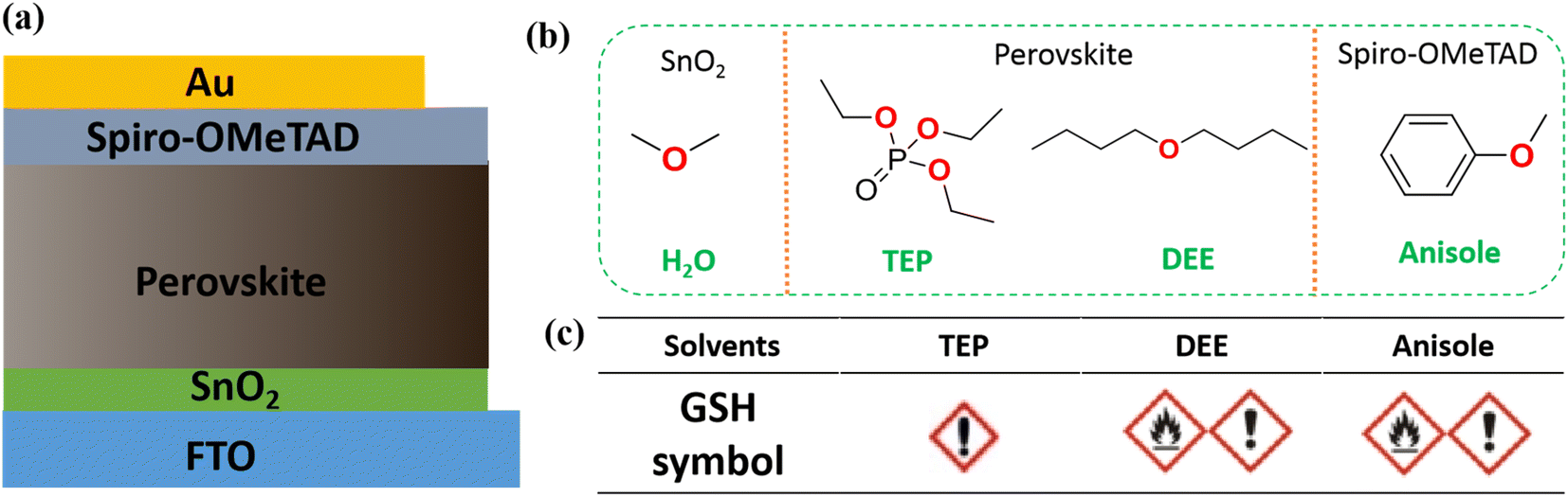 | ||
| Fig. 1 (a) The device structure of typical efficient PSCs. (b) The molecular structure of solvents used for the preparation of various functional layers in the PSCs. (c) The GHS symbols of the solvents. | ||
Fig. 2a shows a photograph of the spiro-OMeTAD solution in different solvents with a concentration of 72.3 mg mL−1. The clear dissolution state demonstrates that the green solvent, anisole, has a comparable dissolution ability to the toxic solvent, CB. Usually, the HTL films in PSC are prepared from spiro-OMeTAD solution with the addition of multifunctional additives, including TBP, Li-TFSI and FK209. Fig. 2b shows a photograph of the spiro-OMeTAD solution with addition of additives. No precipitate occurs after addition of various additives, demonstrating the feasibility of using the green solvent, anisole to replace the toxic CB for the deposition of the HTL layer. Fig. 2c shows the UV-Vis spectra of spiro-OMeTAD solution before the addition of additives. Both absorption spectra exhibit a cut-off at 450 nm, which is consistent with results found in previous reports.14Fig. 2d shows the absorption spectra of the spiro-OMeTAD solution after the addition of additives. Compared with the pristine spiro-OMeTAD solution, the doped spiro-OMeTAD solution exhibits an evident new absorption peak at ∼530 nm. This peak could be attributed to the oxide of spiro-OMeTAD,15 which is a key factor for the fabrication of high-performance solar cells.
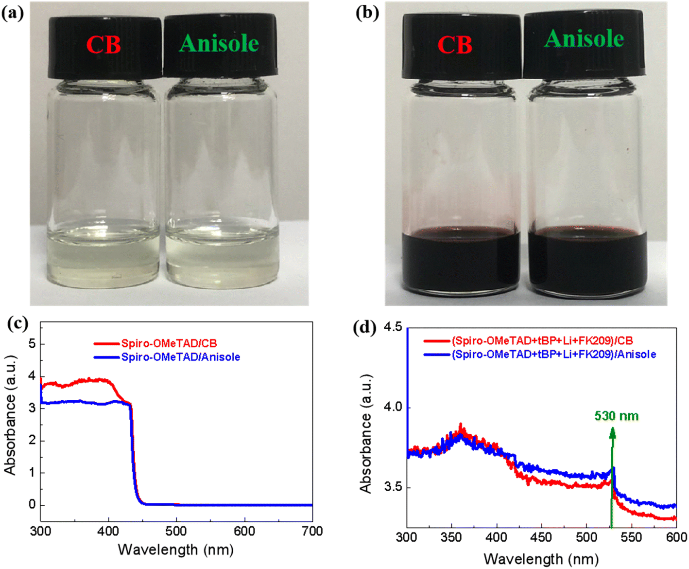 | ||
| Fig. 2 Photographs of spiro-OMeTAD solution in different solvents, (a) pristine spiro-OMeTAD solution, and (b) spiro-OMeTAD + Li-TFSI + TBP + FK209 solution. The UV-Vis absorption spectra of the spiro-OMeTAD in different solvents, (c) pristine spiro-OMeTAD solution, and (d) spiro-OMeTAD + Li-TFSI + TBP + FK209 solution. | ||
Fig. 3a shows the optical microscopy image of perovskite films using the green solvent engineering approach.9 The perovskite films exhibit full coverage and a uniform morphology. Different from the smooth morphology produced by the traditional solvent engineering, the green solvent engineering approach gives the films a wrinkled morphology. The wrinkled morphology of the perovskite films may relate to miscibility between the anti-solvent (DEE) and the host solvent (TEP).16 The full coverage morphology is confirmed by the SEM image (see Fig. 3b). Fig. 3c is the XRD curve of the perovskite films. All the diffraction peaks can be assigned to the α-FAPbI3. Fig. 3d is the UV-Vis absorption spectrum of the perovskite film. It shows a light absorbing ability from 300 nm to ∼806 nm, corresponding to the bandgap of 1.537 eV (see the inset in Fig. 3d). These features of the perovskite films are consistent with the results found in our previous work,9 and provide the possibility for the fabrication of highly efficient solar cells in following work.
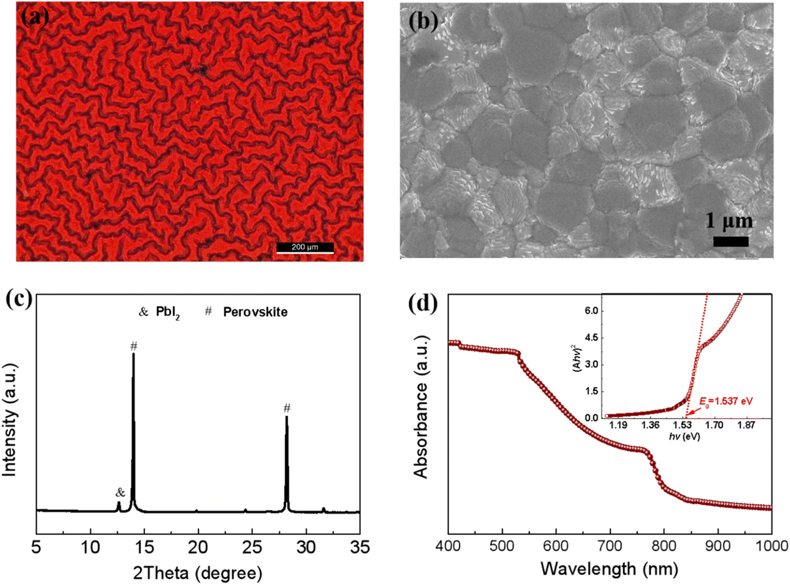 | ||
| Fig. 3 The characterization of the perovskite films prepared by green solvent engineering. (a) An optical microscopy image, (b) the surface SEM image, (c) the XRD curves, and (d) the UV-Vis absorption spectra, where the inset shows the bandgap (Eg) fitting based on the relationship between (Ahν)2–hν. | ||
In addition to the morphology of the perovskite films, the morphology of the spiro-OMeTAD films also plays a key role in achieving highly efficient solar cells. Fig. 4a and b are the optical microscopy images of the spiro-OMeTAD films prepared from CB and anisole, respectively. Similar to the wrinkled morphology of the bottom perovskite films (see Fig. 3a), the spiro-OMeTAD films also exhibit wrinkled morphology. The wrinkled morphology of spiro-OMeTAD films indicates that it forms a conformal contact with the wrinkled perovskite films without delamination.16Fig. 4c and d are the SEM images of spiro-OMeTAD films, which exhibit a uniform and fully covered morphology. However, the spiro-OMeTAD films exhibit some pin holes, which may have side effects on the performance of the solar cells. Fig. 4e and f are the cross-sectional SEM images of different functional layers in the solar cells. The thickness of SnO2 layer, perovskite layer and spiro-OMeTAD layer are ∼25 nm, ∼580 nm and ∼220 nm, respectively. Meanwhile, the cross-sectional SEM images also reconfirm the excellent contact in each of the functional layers.
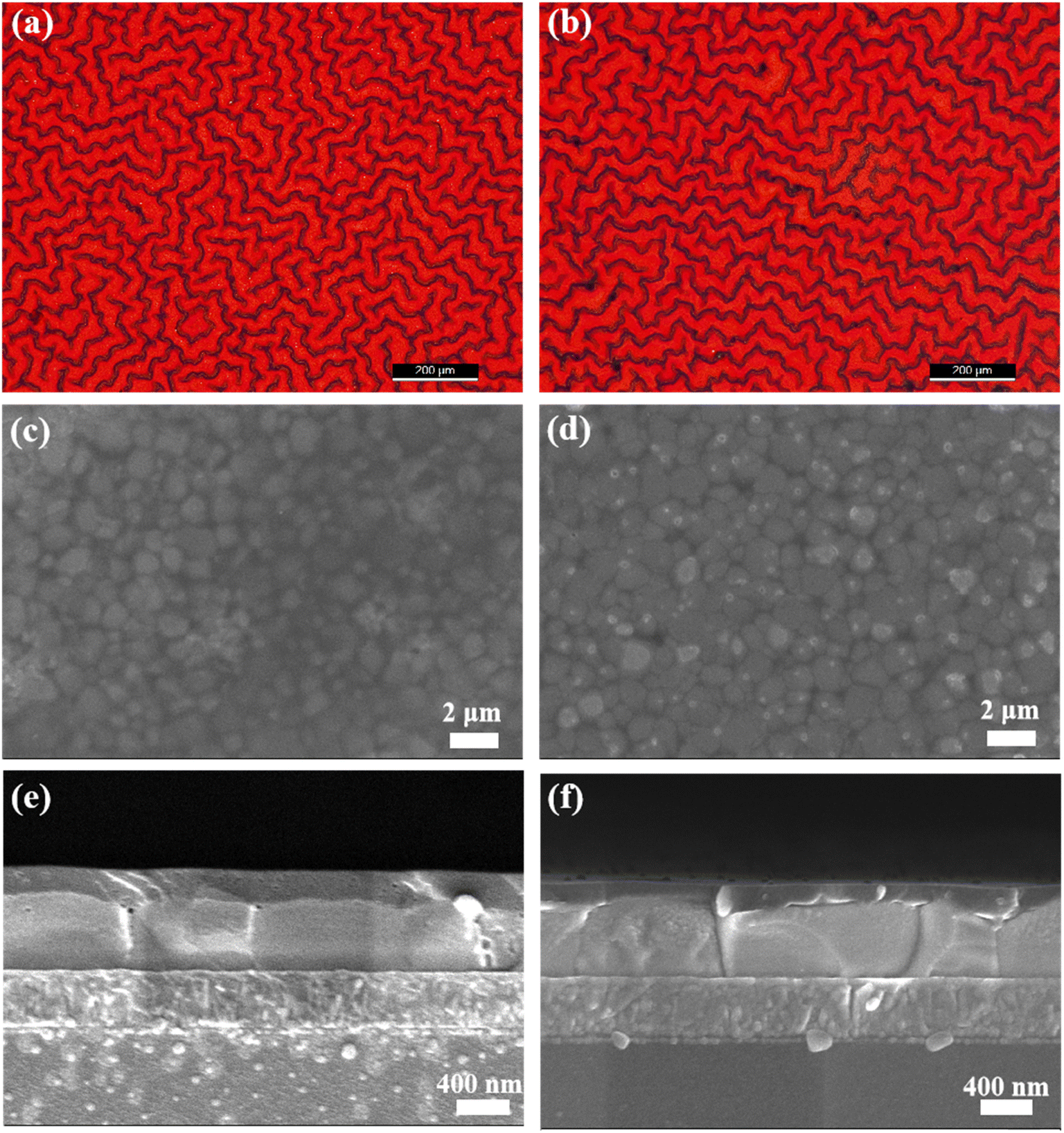 | ||
| Fig. 4 The characterization of spiro-OMeTAD films prepared from CB (left) and anisole (right). (a) and (b) are the optical microscopy images, (c) and (d) are the SEM images of the surface, (e) and (f) are cross-sectional SEM images. | ||
The charge transfer properties in the PSC are strongly dependent on the functional properties. Therefore, we used PL spectra to investigate the effects of the spiro-OMeTAD films on the charge transfer process. As shown in the steady PL spectra (see Fig. 5a), the intensity of the steady PL steady reduces when the spiro-OMeTAD film is deposited onto the perovskite film because of the quenching effects.17Fig. 5b shows the time-resolved photoluminescence (TRPL) and the fitting of the results using a bi-exponential function. As is shown, the average life time of the carriers was significantly reduced from 312.29 ns (without spiro-OMeTAD) to 158.17 ns (after deposition of spiro-OMeTAD from CB), and to 231.25 ns (after deposition of spiro-OMeTAD from anisole) (see Table S1 (ESI†)), respectively. The reduced life time demonstrates that the hole can be effectively transferred from the perovskite films to the HTL of the spiro-OMeTAD films. In particular, it seems that the spiro-OMeTAD films prepared from the green solvent, anisole, have a decreased hole extraction ability that prepared from CB, which is confirmed by the slightly higher intensity in the steady PL (see Fig. 5a), as well as the slightly average long life time in the TRPL spectra (see Table S1, ESI†). In order to explore the reasons for the difference of hole extraction ability of the spiro-OMeTAD films prepared from different solvents, the hole mobility is estimated from the hole-only device by using the space-charge limited current (SCLC) model (see Fig. S2, ESI†), which is described by J = 9ε0εrμV2/8L3 at a higher reversed applied voltage,18 (where ε0 is the vacuum permittivity (8.85 × 10⁻¹² F m−1), εr is the dielectric constant (εr = 25),19μ is the mobility of the charge carrier, V is the effective applied voltage, and L is the thickness of the functional layer (L = 220 nm)). After fitting at a high voltage region, the spiro-OMeTAD film prepared from anisole exhibits a hole mobility of 1.54 × 10⁻⁴ cm2 V−1 s−1, which is lower than the value (3.03 × 10⁻⁴ cm2 V−1 s−1) of the spiro-OMeTAD film prepared from CB. The lower hole mobility may be the reason for the weakened hole transfer ability in the PL spectra.
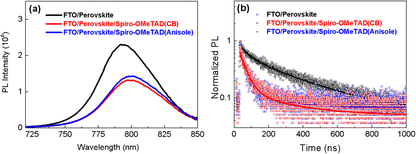 | ||
| Fig. 5 Charge transport properties between the perovskite layer and the spiro-OMeTAD film; (a) steady photoluminescence (PL) spectrum, and (b) time-resolved photoluminescence (TRPL). | ||
In order to check the effect of the spiro-OMeTAD film on the performance of the solar cells, a layer of gold (Au) is deposited onto spiro-OMeTAD films to construct complete PSCs. Fig. 6a shows the light J–V of the best PSC prepared from spiro-OMeTAD films processed with different solvents. The PSCs prepared from CB exhibit an open-circuit voltage (Voc) of 1.0757 V, a short-circuit density (Jsc) of 24.15 mA cm−2, a fill factor (FF) of 0.770, and a power conversion efficiency (PCE) of 20.01% under a reverse scan. In addition, it also shows a Voc of 1.0769 V, a (Jsc) of 24.12 mA cm−2, an FF of 0.750 and a PCE of 19.48% under a forward scan. In contrast, the best solar cell prepared from anisole exhibits a Voc of 1.085 V, a (Jsc) of 24.13 mA cm−2, an FF of 0.726 and a PCE of 19.0% under a reverse scan, and also has a Voc of 1.089 V, (Jsc) of 24.09 mA cm−2, an FF of 0.691 and a PCE of 18.1% under a reverse scan. The statistical results of the photovoltaic parameters are shown in Fig. S2 (ESI†). The slight reduction in performance for the device based on anisole may be from the combination of the low hole mobility (see Fig. S2, ESI†) and the poor morphology (see Fig. 4) of the spiro-OMeTAD films. Both solar cells show an almost negligible hysteresis behavior, which indicates the reliability of the performance of the solar cells. Benefitting from the elimination of the hysteresis behavior, the solar cells deliver a steady output of 20.01% and 18.95% at the maximum power points of PCE-CB and PCE-anisole, respectively (see Fig. 6b). These steady outputs match well with the values obtained from the reverse scan (see Fig. 6a). Fig. 6c shows the IPCE spectra of typical solar cell prepared from different solvents. All the PSCs show a high quantum yield throughout the range from 300 nm to ∼810 nm, corresponding to a bandgap of 1.564 eV by calculating the maximum differential value of IPCE20 (see the inset in Fig. 6c). This value matches well with the value obtained from UV-Vis absorption spectrum (see the inset in Fig. 3d). Fig. 6d shows the evolution of the normalized PCEs of PSCs over the aging time in the glove box. As is shown, the PSCs retains 89.1% and 91.6% of its initial efficiency for the PSCs prepared from CB and anisole, respectively. These results demonstrate that the replacement of CB with anisole can not only solve the solvent toxicity during the processing of the HTL layer, but also maintain the performance without loss for the solar cells, showing it has good prospects for achieve all green solvent solution processed complete solar cells.
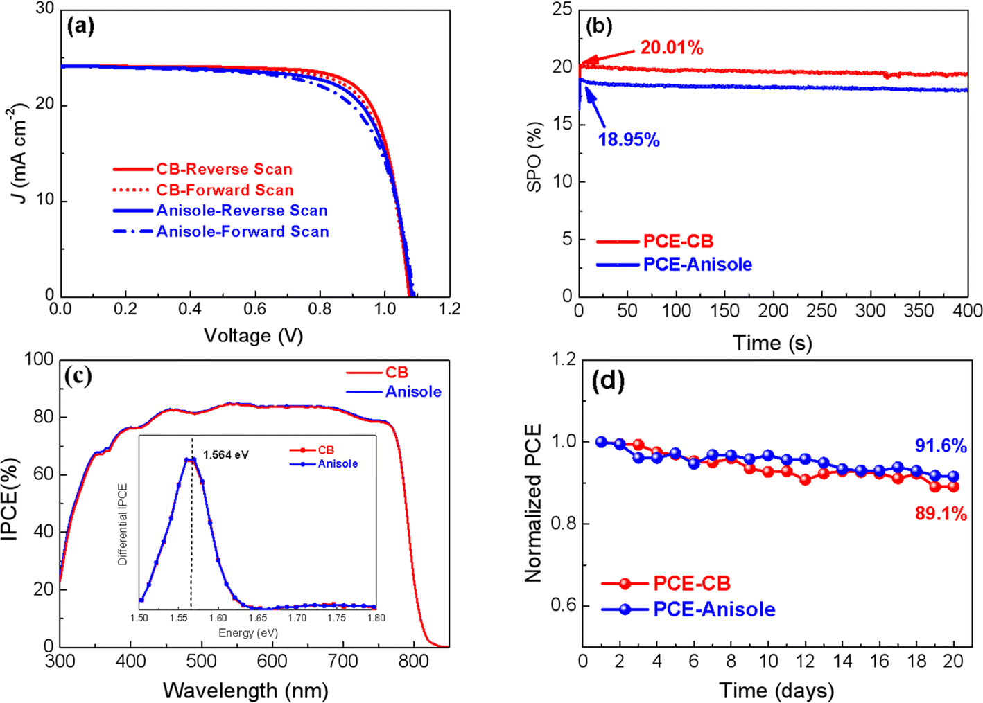 | ||
| Fig. 6 (a) The J–V curves of the best PSCs prepared from spiro-OMeTAD films processed using different solvents. (b) The steady output of the best PSCs, (c) the IPCE spectra, and (d) the stability of PSCs. | ||
4. Conclusions
In conclusion, we screened a green solvent, anisole, to see if it could be used to replace the highly toxic solvent CB for the preparation of spiro-OMeTAD films. Thereafter, we achieved a fully green solvent processed all functional layer for a typical PSC, in which the perovskite films are prepared by using the all green solvent engineering. Compared with the solar cells prepared from the CB processed spiro-OMeTAD films, the solar cells using the green solvent, anisole, to process the spiro-OMeTAD films, exhibit a comparable photovoltaic performance and stability. This research has eliminated the solvent toxicity for the preparation of all functional layers in the most popular solar cell, providing an attractive technological choice to prepare high-performance perovskite solar cells under eco-friendly conditions.Conflicts of interest
There are no conflicts to declare.Acknowledgements
This work was financially supported by Natural Science Foundation of China (Grant No. 52202287 and 51972188), the Science Foundation for High-level Talents of Wuyi University (Grant No. 2019AL001), National College Students' Innovation and Entrepreneurship Training Program (202111349273), the Guangdong Basic and Applied Basic Research Foundation (Grant No. 2020A1515111052 and 2022A1515110497), the Innovation Projects of the Department of Education of Guangdong Province (Grant No. 2022KTSCX142), and the College Innovation Team Project of Guangdong Province (Grant No. 2021KCXTD042).References
- A. Kojima, K. Teshima, Y. Shirai and T. Miyasaka, J. Am. Chem. Soc., 2009, 131, 6050–6051 CrossRef CAS PubMed.
- Y. Zhao, F. Ma, Z. Qu, S. Yu, T. Shen, H. Deng, X. Chu, X. Peng, Y. Yuan, X. Zhang and J. You, Science, 2022, 377, 531–534 CrossRef CAS PubMed.
- J. H. Im, C. R. Lee, J. W. Lee, S. W. Park and N. G. Park, Nanoscale, 2011, 3, 4088–4093 RSC.
- H. S. Kim, C. R. Lee, J. H. Im, K. B. Lee, T. Moehl, A. Marchioro, S. J. Moon, H. Baker, J. H. Yum, J. E. Moser, M. Gratzel and N. G. Park, Sci. Rep., 2012, 2, 591 CrossRef PubMed.
- M. M. Lee, J. Teuscher, T. Miyasaka, T. N. Murakami and H. J. Snaith, Science, 2012, 338, 643–647 CrossRef CAS PubMed.
- N. J. Jeon, J. H. Noh, Y. C. Kim, W. S. Yang, S. Ryu and S. Seok, Nat. Mater., 2014, 13, 897–903 CrossRef CAS PubMed.
- M. Xiao, F. Huang, W. Huang, Y. Dkhissi, Y. Zhu, J. Etheridge, A. Gray-Weale, U. Bach, Y. B. Cheng and L. Spiccia, Angew. Chem., Int. Ed., 2014, 53, 1–7 CrossRef.
- P. J. Holliman, E. W. Jones, A. Connell, S. Ghosh, L. Furnell and R. J. Hobbs, Mater. Res. Innovations, 2019, 7, 508–511 Search PubMed.
- X. Cao, L. Hao, Z. Liu, G. Su, X. He, Q. Zeng and J. Wei, Chem. Eng. J., 2022, 437, 135458 CrossRef CAS.
- X. Liu, Y. Zhang, L. Shi, Z. Liu, J. Huang, J. S. Yun, Y. Zeng, A. Pu, K. Sun, Z. Hameiri, J. A. Stride, J. Seidel, M. A. Green and X. Hao, Adv. Energy Mater., 2018, 8, 1800138 CrossRef.
- T. B Song, Q. Chen, H. Zhou, C. Jiang, H. H. Wang, Y. Yang, Y. Liu, J. You and Y. Yang, J. Mater. Chem. A, 2015, 3, 9032–9050 RSC.
- S. Shan, Y. Li, H. Wu, T. Chen, B. Niu, Y. Zhang, D. Wang, C. Kan, X. Yu, L. Zuo and H. Chen, SusMat, 2021, 1, 537–544 CrossRef CAS.
- R. Wrbitzky, Int. Arch. Occup. Environ. Health, 1999, 72, 19–25 CrossRef CAS PubMed.
- X. Wang, J. Wu, Y. Yang, X. Liu, Q. Guo, Z. Song, G. Li, Z. Lan and M. Huang, J. Mater. Chem. A, 2019, 7, 13256–13264 RSC.
- Y. Yang, J. Wu, X. Liu, Q. Guo, X. Wang, L. Liu, Y. Ding, S. Dai and J. Y. Lin, ACS Appl. Energy Mater., 2019, 2, 2188–2196 CrossRef CAS.
- S. G. Kim, J. H. Kim, P. Ramming, Y. Zhong, K. Schötz, S. J. Kwon, S. Huettner, F. Panzer and N. G. Park, Nat. Commun., 2021, 12, 1554 CrossRef CAS PubMed.
- X. Zhao, H. Shen, Y. Zhang, X. Li, X. Zhao, M. Tai, J. Li, X. Li and H. Lin, ACS Appl. Mater. Interfaces, 2016, 8, 7826–7833 CrossRef CAS PubMed.
- Q. Du, Z. Shen, C. Chen, F. Li, M. Jin, H. Li, C. Dong, J. Zheng, M. Ji and M. Wang, Sol. RRL, 2021, 5, 2100622 CrossRef CAS.
- X. Ji, T. Zhou, X. Ke, W. Wang, S. Wu, M. Zhang, D. Lu, X. Zhang and Y. Liu, J. Mater. Chem. A, 2020, 8, 5163–5170 RSC.
- G. Yang, Z. Ren, K. Liu, M. Qin, W. Deng, H. Zhang, H. Wang, J. Liang, F. Ye, Q. Liang, H. Yin, Y. Chen, Y. Zhuang, S. Li, B. Gao, J. Wang, T. Shi, X. Wang, X. Lu, H. Wu, J. Hou, D. Lei, S. K. So, Y. Yang, G. Fang and G. Li, Nat. Photonics, 2021, 15, 681–689 CrossRef CAS.
Footnote |
| † Electronic supplementary information (ESI) available. See DOI: https://doi.org/10.1039/d3su00146f |
| This journal is © The Royal Society of Chemistry 2023 |