 Open Access Article
Creative Commons Attribution 3.0 Unported Licence
Realizing 18.03% efficiency and good junction characteristics in organic solar cells via hydrogen-bonding interaction between glucose and ZnO electron transport layers†
Zhongqiang
Wang
 *a,
Yabing
Ren
a,
Jiawei
Meng
a,
Xuefeng
Zou
a,
Shenjian
Wang
a,
Min
Zhao
 a,
Hua
Wang
 a,
Yuying
Hao
a,
Bingshe
Xu
a,
Ergang
Wang
a,
Yuying
Hao
a,
Bingshe
Xu
a,
Ergang
Wang
 *b and
Shougen
Yin
 *c
*c
aKey Laboratory of Interface Science and Engineering in Advanced Materials, Ministry of Education, Research Center of Advanced Materials Science and Technology, Taiyuan University of Technology, Taiyuan, 030024, China. E-mail: wangzhongqiang@tyut.edu.cn
bDepartment of Chemistry and Chemical Engineering, Chalmers University of Technology, Göteborg, SE-412 96, Sweden. E-mail: ergang@chalmers.se
cKey Laboratory of Display Materials and Photoelectric Devices (Ministry of Education), School of Materials Science and Engineering, Tianjin University of Technology, Tianjin 300384, China. E-mail: sgyin@tjut.edu.cn
First published on 19th December 2022
Abstract
Electron transport layers (ETLs) with excellent electron extraction capability are essential for realizing high efficiency in organic solar cells (OSCs). A sol–gel-processed ZnO ETL is widely used in OSCs due to its high mobility and suitable work function. However, the existence of defects usually results in low photovoltaic performance during the operation of OSCs. In this work, glucose (Gl) was used to passivate free OH traps via hydrogen-bonding interaction and formed ZnO/Gl ETLs with ZnO, which exhibited improved electron extraction capability and reduced trap defect density. Thus, a champion efficiency of 18.03% was obtained in a PM6:Y6 light absorber-based cell, which is >11% higher than that of the reference cell (16.15%) with a pristine ZnO ETL. Impressive enhancements by >11% were also observed in different fullerene and non-fullerene light absorber-based cells relative to that of the reference cell. This study demonstrates a new strategy to design ETLs for realizing high efficiency in OSCs.
1. Introduction
Organic solar cells (OSCs) have attracted great attention due to their advantages such as mechanical flexibility, light weight, and solution processing over their inorganic counterparts.1–4 Recently, the power conversion efficiency (PCE) of OSCs has surpassed 19% in single-junction cells.5–9 The significant progress in OSCs can be attributed to the development of organic semiconductors covering a wide range of the solar spectrum, the optimization of device structures and deep understanding of device physics.10–13 To realize efficient light-to-electron conversion, hole transport layers (HTLs) and electron transport layers (ETLs) that can facilitate charge extraction and transport play important roles, apart from the light absorbers responsible for exciton generation and dissociation, and charge transport.14 Hence, the development of suitable HTLs and ETLs is critical to achieving good junction characteristics and high efficiency in OSCs.Compared to the conventional OSC device structure of glass/ITO/PEDOT:PSS/light absorbers/ETL/Al, an inverted structure, i.e., glass/ITO/ETL/light absorbers/HTL/Al, possesses reverse junction polarity, which usually shows higher PCE and better lifetime in OSCs. To construct efficient OSCs with an inverted structure, excellent ETLs such as ZnO, SnO2, TiOx, and CsOx exhibit good transparence, high electron mobility and suitable work function (WF).15–18 ZnO is widely used as an ETL material due to its excellent optical and electrical properties, good film-forming properties, and low annealing temperature.19–21 The sol–gel technique is a simple and effective method that is used to deposit ZnO ETLs. However, sol–gel-processed ZnO ETLs show surface and inside defects, such as Zn interstitials, free hydroxide (–OH), and oxygen vacancies, which lead to inferior electrical properties.22–24 These defects in ZnO ETLs act as trap centers in OSCs, resulting in low photovoltaic performance and inferior junction characteristics. Hence, it is essential to develop an efficient passivation strategy to reduce defects for achieving good charge extraction characteristics and high efficiency in OSCs with sol–gel-processed ZnO ETLs.
In this contribution, we demonstrate an excellent ETL which was processed by depositing glucose (Gl) on top of sol–gel-processed ZnO films. Our study proved that the deposition of Gl could passivate surface defects of free OH groups due to the hydrogen bond interaction between ZnO and Gl. Thus, good junction properties and high efficiency were achieved from ZnO/Gl ETL-based OSCs. A low-cost and facile strategy was developed to form highly efficient ETLs for OSCs.
2. Results and discussion
X-ray photoelectron spectroscopy (XPS) was used to unravel the interaction between ZnO and Gl films. The XPS spectra of ZnO and ZnO/Gl are shown in Fig. 1a and ESI Fig. S2.† The binding energy peak at 288.88 eV corresponds to the C![[double bond, length as m-dash]](https://www.rsc.org/images/entities/char_e001.gif) O group. This peak shifted to 288.58 eV after the deposition of Gl, which signifies interaction between ZnO and Gl.
O group. This peak shifted to 288.58 eV after the deposition of Gl, which signifies interaction between ZnO and Gl.
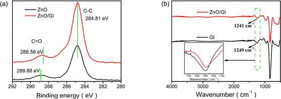 | ||
| Fig. 1 (a) XPS spectra of ZnO and ZnO/Gl films and (b) FTIR spectra of Gl and ZnO/Gl films (the inset shows enlarged FTIR absorption bands in the range 1375–1140 cm−1). | ||
The FTIR spectra of Gl and ZnO/Gl are shown in Fig. 1b. According to the literature, the absorption peak at around 1249 cm−1 from the pristine Gl sample is due to OH vibration.25 This peak was shifted to 1241 cm−1 after the deposition of Gl on the ZnO film, which indicated that the O–H vibration was influenced by the formation of a hydrogen bond between CO in Gl and the free OH on the surface of ZnO. The CO and OH groups form hydrogen bonds because of the electron transfer from CO to OH.26 The trap sites caused by free OH in sol–gel ZnO could obviously be reduced by hydrogen-bonding interactions between CO and OH groups. The trap passivation should have improved the electron extraction and transport properties of the ZnO ETL. It was expected that free OH passivation of ZnO could lead to impressive photovoltaic performance in Gl-passivated ZnO ETL-based cells.
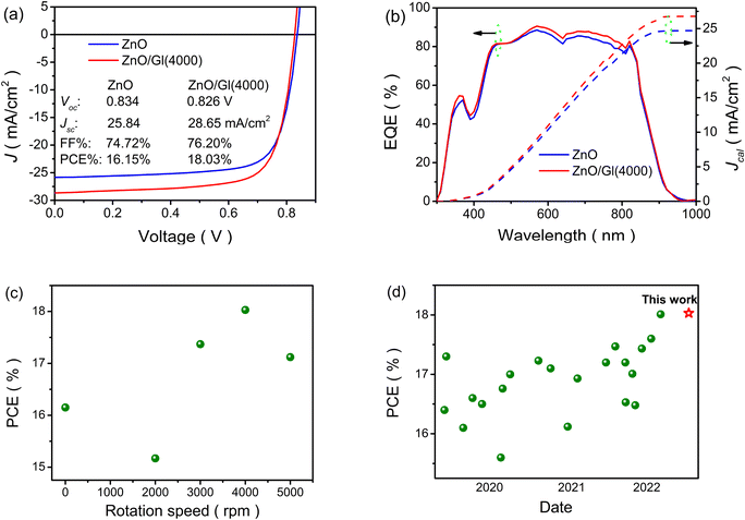
The thickness of ZnO ETLs was fixed to be 40 nm based on our previous work.27 The Gl-modified ZnO ETLs were named ZnO/Gl(X) (X stands for the spin speed). To obtain the optimal photovoltaic performance, the thicknesses of Gl were tuned by varying the spin speed from 2000 to 5000 rpm under a Gl concentration of 2 mg mL−1. The current density–voltage (J–V) curves and external quantum efficiency (EQE) spectra are shown in Fig. 2a, b and S3.† As displayed in Fig. 2a, a PCE of 16.15% with an open circuit voltage (Voc) of 0.834 V, a short circuit current density (Jsc) of 25.84 mA cm−2, and a fill factor (FF) of 74.72% was obtained from the PM6:Y6 light absorber-based cell with a pristine ZnO ETL, which is in good agreement with reported values.24 It is clear that the cells showed higher PCE when the spin speeds were over 4000 rpm compared to the reference cell. Due to the insulation of Gl, decreased PCEs were recorded when the Gl spin speed was lower than 4000 rpm, as shown in Fig. 2c. The highest PCE of 18.03%, with a Voc of 0.826 V, a Jsc of 28.65 mA cm−2, and a FF of 76.20%, was achieved from cells with the ZnO/Gl(4000) ETL, which is an improvement by 11% relative to that of the reference cell with a ZnO ETL due to the increase in Jsc and FF, as summarized in Table 1. The reported PCEs based on the PM6:Y6 blend are summarized in Fig. 2d. To the best of our knowledge, the PCE achieved in this work is one of the highest values recorded from PM6:Y6 binary light absorber-based OSCs.
| ETLs | V oc (V) | J sc (mA cm−2) | FF (%) | PCE (%) |
|---|---|---|---|---|
| a The light absorber is a non-fullerene blend of PM6:Y6. | ||||
| ZnO | 0.833 ± 0.003 | 24.59 ± 1.25 | 73.41 ± 1.31 | 16.00 ± 0.15 |
| 0.834 | 25.84 | 74.72 | 16.15 | |
| ZnO/Gl(2000) | 0.817 ± 0.003 | 25.53 ± 1.33 | 67.37 ± 1.50 | 14.93 ± 0.24 |
| 0.820 | 26.86 | 68.87 | 15.17 | |
| ZnO/Gl(3000) | 0.824 ± 0.003 | 27.11 ± 1.28 | 72.56 ± 1.46 | 17.16 ± 0.21 |
| 0.827 | 28.39 | 74.02 | 17.37 | |
| ZnO/Gl(4000) | 0.824 ± 0.003 | 27.35 ± 1.30 | 74.75 ± 1.45 | 17.83 ± 0.20 |
| 0.826 | 28.65 | 76.20 | 18.03 | |
| ZnO/Gl(5000) | 0.823 ± 0.003 | 26.37 ± 1.29 | 73.60 ± 1.30 | 17.01 ± 0.11 |
| 0.826 | 27.66 | 74.90 | 17.12 | |
As displayed in Fig. 2b, the cell with the ZnO/Gl(4000) ETL showed the highest photo-response especially in the near-infrared region, which resulted in improved Jcal. The enhancement in EQE spectra was in line with the variation of Jsc extracted from J–V curves, which proved the enhancement in the performances of cells with ZnO/Gl(X) ETLs.
The morphology of ETLs has a significant impact on the interfacial contact and charge transfer in OSCs.28 Atomic force microscopy (AFM) was used to investigate the morphology variation of the ZnO ETL before and after Gl deposition. The two-dimensional (2-D) and the corresponding three-dimensional (3-D) AFM images are displayed in Fig. 3. As depicted in Fig. 3a and b, root-mean-square (RMS) roughness values of 0.512 and 0.318 nm were obtained from the pristine and Gl-modified ZnO films, respectively. The smooth surface of ZnO/Gl(X) ETLs would be of great benefit to the photovoltaic performance and junction characteristics of the OSCs.
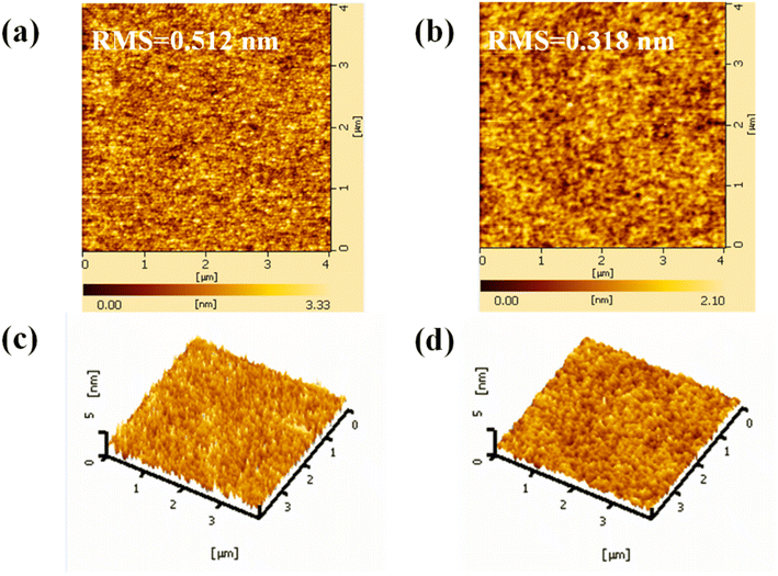 | ||
| Fig. 3 Two-dimensional (2-D) AFM images (4.0 × 4.0 μm2) of ZnO (a) and ZnO/Gl(4000) ETLs (b), and 3-D AFM images (4.0 × 4.0 μm2) of ZnO (c) and ZnO/Gl(4000) ETLs (d). | ||
Good junction characteristics are necessary for achieving high photovoltaic performance in OSCs. To evaluate the junction properties, the ideal diode equation was used to analyze the J–V characteristics of cells with ZnO and ZnO/Gl(X) ETLs without illumination, which is expressed as:
 | (1) |
Without illumination (Jph = 0), eqn (1) can be simplified as:
 | (2) |
The parameters of n, J0, Rsh, and Rs can be evaluated by fitting J–V curves with eqn (2). The dark state J–V curves obtained from cells with ZnO and ZnO/Gl(4000) ETLs are plotted in Fig. 4. The evaluated parameters are also summarized in Fig. 4. It has been proved that n is highly related to the interfaces of solar cells. A decreased n of 1.62 was obtained from a ZnO/Gl(4000) ETL-based cell, whereas n was found to be 2.01 for the cell with the ZnO ETL, which indicated better junction properties in this cell.
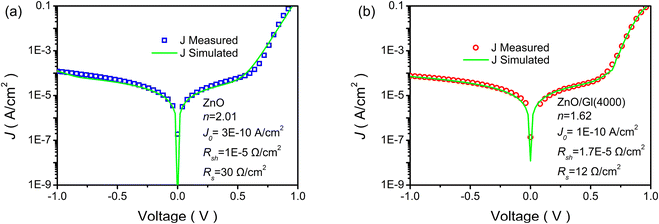 | ||
| Fig. 4 Measured (blue squares or red circles) and simulated (green solid lines) J–V curves without illumination: (a) cell with the pristine ZnO ETL and (b) cell with the ZnO/Gl(4000) ETL. | ||
J 0 is part of the reverse current density in diodes, which is independent of reverse bias. A low J0 means that ZnO ETLs possess excellent hole blocking capability.29 In comparison with the reference cell with a J0 of 3 × 10⁻¹⁰ A cm−2, the cell with ZnO/Gl(4000) as the ETL showed a lower J0 of 1 × 10⁻¹⁰ A cm−2, as depicted in Fig. 4. The decreased J0 value indicated superior hole blocking capability of Gl-modified ZnO, which further confirmed the good junction characteristics in these cells. The superior hole blocking capability contributed to the improved FF in OSCs.
To understand the defect-assisted recombination process, electron-only devices with different ETLs were made to analyze the voltage of the trap-filled limit (VTFL). As shown in Fig. 5a, three different regions are observed in the double-log![[thin space (1/6-em)]](https://www.rsc.org/images/entities/char_2009.gif) J–V curves of electron-only devices. In the TFL region, all traps are filled with the injected carriers, which could reflect the defect passivation of ZnO ETLs. A reduced VTFL of 0.63 V was obtained from the cell with the ZnO/Gl(4000) ETL, suggesting that the introduction of Gl reduced the defect density of ZnO. The suppressed trap-assisted recombination was beneficial to realizing efficient electron extraction and transport in ZnO/Gl(X) ETL-based cells, resulting in improved Jsc and FF.
J–V curves of electron-only devices. In the TFL region, all traps are filled with the injected carriers, which could reflect the defect passivation of ZnO ETLs. A reduced VTFL of 0.63 V was obtained from the cell with the ZnO/Gl(4000) ETL, suggesting that the introduction of Gl reduced the defect density of ZnO. The suppressed trap-assisted recombination was beneficial to realizing efficient electron extraction and transport in ZnO/Gl(X) ETL-based cells, resulting in improved Jsc and FF.
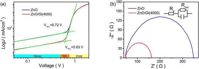 | ||
| Fig. 5 (a) Electron-only devices with pristine ZnO and ZnO/Gl(4000) ETLs and (b) EIS spectra of cells with pristine ZnO and ZnO/Gl(4000) ETLs (the inset represents the equivalent circuit). | ||
To further study the influence of Gl, electrical impedance spectroscopy (EIS) was utilized to compare the electrical characteristics of cells with different ETLs,30 as plotted in Fig. 5b. The transport resistance was extracted from the EIS spectra by fitting with the equivalent circuit. It was clear that the cell with the ZnO/Gl(4000) ETL exhibited a shorter diameter compared to that of the cell with the pristine ZnO ETL. The short diameter meant low transport resistance, which also contributed to the enhanced photovoltaic performance in cells with ZnO/Gl(X) ETLs.
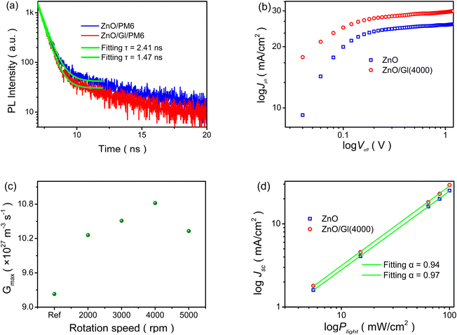
The electron extraction capability of ETLs is directly affected by the charge transport and extraction processes in OSCs, which can be analyzed by the exciton decay dynamics of time-resolved photoluminescence (TRPL) spectra,31 as shown in Fig. 6a. The extracted lifetimes from the samples of ZnO/PM6 and ZnO/Gl(4000)/PM6 were 2.41 and 1.47 ns, respectively. The decreased lifetime meant better electron extraction capability of the ZnO/Gl(4000) ETL compared to the ZnO ETL, resulting in efficient charge extraction and transport processes in ZnO/Gl(X) ETL-based cells.
Moreover, photocurrent densities (Jph) under different effective voltages (Veff) of cells were compared to reveal the exciton generation behavior.32,33Fig. 6b and S4† show the plots of log![[thin space (1/6-em)]](https://www.rsc.org/images/entities/char_2009.gif) Jphversus log
Jphversus log![[thin space (1/6-em)]](https://www.rsc.org/images/entities/char_2009.gif) Veff. The maximum exciton generation rate (Gmax) of cells was calculated from the plots of log Jph–log
Veff. The maximum exciton generation rate (Gmax) of cells was calculated from the plots of log Jph–log![[thin space (1/6-em)]](https://www.rsc.org/images/entities/char_2009.gif) Veff, as summarized in Fig. 6c. A clear enhancement in Gmax was observed in cells with ZnO/Gl(X) ETLs. This result indicates efficient light photon absorption in cells using ZnO/Gl(X) as ETLs, which could contribute to improved Jsc in these cells.
Veff, as summarized in Fig. 6c. A clear enhancement in Gmax was observed in cells with ZnO/Gl(X) ETLs. This result indicates efficient light photon absorption in cells using ZnO/Gl(X) as ETLs, which could contribute to improved Jsc in these cells.
The dependence of Jsc on incident light intensity (Plight) was investigated to reveal charge recombination behaviors in cells with different ETLs.34Fig. 6d and S7† display the plots of the log Jscversus log![[thin space (1/6-em)]](https://www.rsc.org/images/entities/char_2009.gif) Plight of cells with ZnO and ZnO/Gl(4000) ETLs. The power law exponent of α was obtained by linear fitting and α values of 0.94 and 0.97 were extracted from the reference cell with the ZnO ETL and the cell with the ZnO/Gl(4000) ETL, respectively. The increased α (close to 1) in the ZnO/Gl(4000) ETL-based cell indicated less bimolecular recombination loss,35 which helped to realize improved Jsc, FF and PCE in ZnO/Gl(X) ETL-based cells.
Plight of cells with ZnO and ZnO/Gl(4000) ETLs. The power law exponent of α was obtained by linear fitting and α values of 0.94 and 0.97 were extracted from the reference cell with the ZnO ETL and the cell with the ZnO/Gl(4000) ETL, respectively. The increased α (close to 1) in the ZnO/Gl(4000) ETL-based cell indicated less bimolecular recombination loss,35 which helped to realize improved Jsc, FF and PCE in ZnO/Gl(X) ETL-based cells.
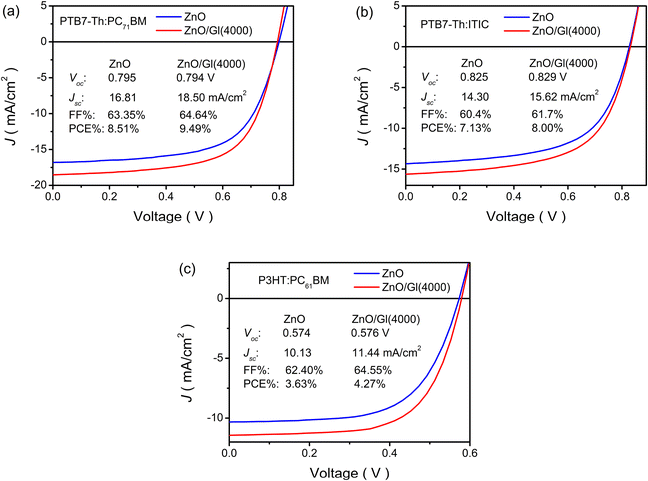
The ZnO/Gl(X) ETLs were also applied in blends of PTB7-Th:PC71BM, PTB7-Th:ITIC, and P3HT:PC61BM light absorber-based OSCs. Impressive enhancements were observed in these cells after the introduction of Gl. As shown in Fig. 7 and Table S2,† >11% enhancements were obtained from these light absorber-based cells after the insertion of Gl compared to the reference cell with the ZnO ETL. These results demonstrated the general applicability of ZnO/Gl(X) as an ETL in fullerene and non-fullerene light absorber-based OSCs.
3. Conclusions
In conclusion, Gl was inserted between a ZnO ETL and light absorbers in inverted OSCs. Due to the hydrogen-bonding interaction between CO and OH groups, the insertion of Gl not only smoothened the interfacial contact, but also passivated OH caused surface defects on the ZnO film. Furthermore, the introduction of Gl improved the junction characteristics, contributed to electron extraction and transport processes, and suppressed bimolecular recombination loss in OSCs. In PM6:Y6 light absorber-based cells, a champion efficiency of 18.03% was obtained, which is >11% higher than that of the reference cell (16.15%). Impressive enhancements (>11%) were also observed in different fullerene and non-fullerene blend light absorber (PTB7-Th:PC71BM, PTB7-Th:ITIC, and P3HT:PC61BM)-based cells, which proved the general applicability of ZnO/Gl(X) as ETLs. A novel strategy by applying Gl on top of ZnO was demonstrated to design highly efficient ETLs for OSCs.Author contributions
Zhongqiang Wang: experimental design, data analysis, writing, and funding acquisition. Yabing Ren, Jiawei Meng, Xuefeng Zou, and Shenjian Wang: experimental operation, data curation, and data validation. Min Zhao: data analysis and funding acquisition. Hua Wang, Yuying Hao, and Bingshe Xu: resources and project administration. Ergang Wang: data analysis, funding acquisition, manuscript review and editing. Shougen Yin: resources and supervision. All authors contributed to the final polishing of the manuscript.Conflicts of interest
There are no conflicts to declare.Acknowledgements
This work was supported by the Shanxi Provincial Natural Science Foundation of China (Grant No. 20210302123149 and 20210302123115) and Research Project Supported by Shanxi Scholarship Council of China (Grant No. 2022-046). This work was carried out with the support of the Open Foundation of Key Laboratory of Display Materials and Photoelectric Devices of Tianjin University of Technology. E. W. thanks the Swedish Research Council (2016-06146 and 2019-02345), the Swedish Research Council Formas, the Knut and Alice Wallenberg Foundation (2017.0186 and 2016.0059) and the Swedish Energy Agency (P2021-90067) for financial support.References
- Y. Li, X. Huang, K. Ding, H. K. M. Sheriff, L. Ye, H. Liu, C.-Z. Li, H. Ade and S. R. Forrest, Nat. Commun., 2021, 12, 5419 CrossRef CAS PubMed
.
- C. Li, J. Zhou, J. Song, J. Xu, H. Zhang, X. Zhang, J. Guo, L. Zhu, D. Wei, G. Han, J. Min, Y. Zhang, Z. Xie, Y. Yi, H. Yan, F. Gao, F. Liu and Y. Sun, Nat. Energy, 2021, 6, 605–613 CrossRef CAS
.
- Y. Zhang, Y. Ji, Y. Zhang, W. Zhang, H. Bai, M. Du, H. Wu, Q. Guo and E. Zhou, Adv. Funct. Mater., 2021, 32, 2205115 CrossRef
.
- P. Bi, S. Zhang, Z. Chen, Y. Xu, Y. Cui, T. Zhang, J. Ren, J. Qin, L. Hong, X. Hao and J. Hou, Joule, 2021, 5, 2408–2419 CrossRef CAS
.
- R. Sun, Y. Wu, X. Yang, Y. Gao, Z. Chen, K. Li, J. Qiao, T. Wang, J. Guo, C. Liu, X. Hao, H. Zhu and J. Min, Adv. Mater., 2022, 34, 2110147 CrossRef CAS
.
- Y. Cui, Y. Xu, H. Yao, P. Bi, L. Hong, J. Zhang, Y. Zu, T. Zhang, J. Qin, J. Ren, Z. Chen, C. He, X. Hao, Z. Wei and J. Hou, Adv. Mater., 2021, 33, 2102420 CrossRef CAS
.
- L. Zhu, M. Zhang, J. Xu, C. Li, J. Yan, G. Zhou, W. Zhong, T. Hao, J. Song, X. Xue, Z. Zhou, R. Zeng, H. Zhu, C.-C. Chen, R. Mackenzie, Y. Zou, J. Nelson, Y. Zhang, Y. Sun and F. Liu, Nat. Mater., 2022, 21, 656–663 CrossRef CAS
.
- C. He, Y. Pan, Y. Ouyang, Q. Shen, Y. Gao, K. Yan, J. Fang, Y. Chen, C.-Q. Ma, J. Min, C. Zhang, L. Zuo and H. Chen, Energy Environ. Sci., 2022, 15, 2537–2544 RSC
.
- K. Chong, X. Xu, H. Meng, J. Xue, L. Yu, W. Ma and Q. Peng, Adv. Mater., 2022, 34, 2109516 CrossRef CAS
.
- J. Song and Z. Bo, Sci. China Chem., 2019, 6, 9–13 CrossRef
.
- Q. Nie, A. Tang, Q. Guo and E. Zhou, Nano Energy, 2021, 87, 106174 CrossRef CAS
.
- Y. Liu, J. Song and Z. Bo, Chem. Commun., 2021, 57, 302–314 RSC
.
- H. Meng, C. Liao, M. Deng, X. Xu, L. Yu and Q. Peng, Angew. Chem., Int. Ed., 2021, 60, 22554–22561 CrossRef CAS
.
- X. Cai, T. Yuan, X. Liu and G. Tu, ACS Appl. Mater. Interfaces, 2017, 9, 36082–36089 CrossRef CAS
.
- H. Gao, X. Wei, R. Yu, F.-Y. Cao, Y. Gong, Z. Ma, Y.-J. Cheng, C.-S. Hsu and Z. Tan, Adv. Opt. Mater., 2022, 10, 2102031 CrossRef CAS
.
- K. Pandi, K. Peramaiah and B. Neppolian, ACS Appl. Energy Mater., 2021, 4, 11480–11487 CrossRef CAS
.
- Y. Tao, H. Liu, D. Wang, F. Zhao, Z. Chen, H. Zhu, H. Chen and C.-Z. Li, Infomat, 2022, 4, e12276 CrossRef CAS
.
- X. Zhou, X. Fan, X. Sun, Y. Zhang and Z. Zhu, Nanoscale Res. Lett., 2015, 10, 29 CrossRef PubMed
.
- C. Hou and H. Yu, Chem. Eng. J., 2021, 407, 127192 CrossRef CAS
.
- J. Zheng, Y. Luo, X. Wen, Q. Zhang, Y. Song, J. Zhou, N. Jiang, L. Liu, F. Huang and Z. Xie, J. Mater. Chem. A, 2021, 9, 9616–9623 RSC
.
- G. K. Poduval, L. Duan, M. A. Hossain, B. Sang, Y. Zhang, Y. Zou, A. Uddin and B. Hoex, Sol. RRL, 2020, 4, 2000241 CrossRef CAS
.
- X. Liu, Z. Zheng, J. Wang, Y. Wang, B. Xu, S. Zhang and J. Hou, Adv. Mater., 2022, 34, 2106453 CrossRef CAS
.
- C.-Z. Li, J. Huang, H. Ju, Y. Zang, J. Zhang, J. Zhu, H. Chen and A. K.-Y. Jen, Adv. Mater., 2016, 28, 7269–7275 CrossRef CAS PubMed
.
- M. Cui, D. Li, X. Du, N. Li, Q. Rong, N. Li, L. Shui, G. Zhou, X. Wang, C. J. Brabec and L. Nian, Adv. Mater., 2020, 32, 2002973 CrossRef CAS PubMed
.
- N. S. Inamuddin, M. I. Ahamed, S. Kanchi and H. A. Kashmery, Sci. Rep., 2020, 10, 5052 CrossRef CAS
.
- S. Zhou, X. Zheng, X. Yu, J. Wang, J. Weng, X. Li, B. Feng and M. Yin, Chem. Mater., 2007, 19, 247–253 CrossRef CAS
.
- R. Zhang, M. Zhao, Z. Wang, Z. Wang, B. Zhao, Y. Miao, Y. Zhou, H. Wang, Y. Hao, G. Chen and F. Zhu, ACS Appl. Mater. Interfaces, 2018, 10, 4895–4903 CrossRef CAS
.
- D. Zhou, Y. Qin, R. Zhong, H. Xu, Y. Tong, B. Hu and Y. Xie, J. Mater. Sci.: Mater. Electron., 2018, 29, 18458–18464 CrossRef CAS
.
- Y. Chen, C. Lin, T. Guo and T. Wen, ACS Appl. Mater. Interfaces, 2018, 10, 26805–26811 CrossRef CAS
.
- C. Huang and H. Yu, ACS Appl. Mater. Interfaces, 2020, 12, 19643–19654 CrossRef CAS PubMed
.
- A. Classen, C. L. Chochos, L. Lueer, V. G. Gregoriou, J. Wortmann, A. Osvet, K. Forberich, I. McCulloch, T. Heumueller and C. J. Brabec, Nat. Energy, 2020, 5, 711–719 CrossRef CAS
.
- S. Lee, Y. Kim, D. Kim, D. Jeong, G.-U. Kim, J. Kim and B. J. Kim, Macromolecules, 2021, 54, 7102–7112 CrossRef CAS
.
- X. Xiong, X. Xue, M. Zhang, T. Hao, Z. Han, Y. Sun, Y. Zhang, F. Liu, S. Pei and L. Zhu, ACS Energy Lett., 2021, 6, 3582–3589 CrossRef CAS
.
- S. Jung, J. Lee, U. Kim and H. Park, Sol. RRL, 2019, 4, 1900420 CrossRef
.
- J. Yu, Y. Xi, C.-C. Chueh, J.-Q. Xu, H. Zhong, F. Lin, S. B. Jo, L. D. Pozzo, W. Tang and A. K.-Y. Jen, Nano Energy, 2017, 39, 454–460 CrossRef CAS
.
Footnote |
† Electronic supplementary information (ESI) available: Experimental section; device architecture of OSCs; chemical structures of PTB7-Th, PC71BM, PM6, Y6, and glucose; XPS spectra of Gl and ZnO/Gl; J–V characteristics of cells using different ETLs; log![[thin space (1/6-em)]](https://www.rsc.org/images/entities/char_2009.gif) Jphversus log Jphversus log![[thin space (1/6-em)]](https://www.rsc.org/images/entities/char_2009.gif) Veff of cells using different ETLs; P(E,T) versus log Veff of cells using different ETLs; P(E,T) versus log![[thin space (1/6-em)]](https://www.rsc.org/images/entities/char_2009.gif) Veff of cells using different ETLs; P(E,T) obtained from cells with different ETLs; log Veff of cells using different ETLs; P(E,T) obtained from cells with different ETLs; log![[thin space (1/6-em)]](https://www.rsc.org/images/entities/char_2009.gif) Jscversus log Jscversus log![[thin space (1/6-em)]](https://www.rsc.org/images/entities/char_2009.gif) Plight of OSCs with ZnO and ZnO/Gl(X) ETLs; Vocversus log Plight of OSCs with ZnO and ZnO/Gl(X) ETLs; Vocversus log![[thin space (1/6-em)]](https://www.rsc.org/images/entities/char_2009.gif) Plight of OSCs with ZnO and ZnO/Gl(X) ETLs; photovoltaic parameters extracted from J–V curves. See DOI: https://doi.org/10.1039/d2ta07856b Plight of OSCs with ZnO and ZnO/Gl(X) ETLs; photovoltaic parameters extracted from J–V curves. See DOI: https://doi.org/10.1039/d2ta07856b |
| This journal is © The Royal Society of Chemistry 2023 |

