
Colloidal quantum dot materials for next-generation near-infrared optoelectronics
Lingju
Meng
 ab,
Qiwei
Xu
c,
Jiangwen
Zhang
c and
Xihua
Wang
*c
ab,
Qiwei
Xu
c,
Jiangwen
Zhang
c and
Xihua
Wang
*c
aDepartment of Applied Physics, Aalto University, Espoo, Finland
bDepartment of Chemistry and Materials Science, Micronova Nanofabrication Centre, Aalto University, Espoo, Finland
cDepartment of Electrical and Computer Engineering, University of Alberta, Edmonton, Canada. E-mail: xihua@ualberta.ca
First published on 12th December 2023
Abstract
Colloidal quantum dots (CQDs) are a promising class of materials for next-generation optoelectronic devices, such as displays, LEDs, lasers, photodetectors, and solar cells. CQDs can be obtained at low cost and in large quantities using wet chemistry. CQDs have also been produced using various materials, such as CdSe, InP, perovskites, PbS, PbSe, and InAs. Some of these CQD materials absorb and emit photons in the visible region, making them excellent candidates for displays and LEDs, while others interact with low-energy photons in the near-infrared (NIR) region and are intensively utilized in NIR lasers, NIR photodetectors, and solar cells. In this review, we have focused on NIR CQD materials and reviewed the development of CQD materials for solar cells, NIR lasers, and NIR photodetectors since the first set of reports on CQD materials in these particular applications.
 Lingju Meng | Dr Lingju Meng received his BS degree in Applied Physics from the University of Science and Technology of China, P. R. China in 2013, and PhD degree in Solid State Electronics from the University of Alberta, Canada in 2020. From 2013 to 2020, he was a Research Assistant in the Department of Electrical and Computer Engineering, University of Alberta. Since 2021, he has been a Postdoctoral Researcher at Aalto University, Finland. His research interests include electronic/optoelectronic devices based on colloidal quantum dots, micro/nanoelectromechanical sensors, and nanofabrication techniques. |
 Qiwei Xu | Dr Qiwei Xu holds his bachelor's degree in Applied Physics from the Beijing University of Posts and Telecommunications in 2016 and received his PhD in Microsystems and Nanodevices from the University of Alberta in 2023. His research interests are utilizing nanostructures for photonics applications. Essentially, he focuses on developing highly efficient and stable optoelectronic devices, such as photodetectors, based on colloidal quantum dots. |
 Jiangwen Zhang | Jiangwen Zhang works on colloidal quantum dot optoelectronic devices. She received her BSc degree from Huazhong University of Science and Technology in 2019 and her MSc degree in Phonics and Plasmas from the University of Alberta in 2022. She joined Dr Xihua Wang's research group as a PhD student in September 2022. |
 Xihua Wang | Dr Xihua Wang works on colloidal quantum dot and cellulose nanocrystal based electronic and photonic devices, as well as micro-/nanostructured devices for sensing and energy harvesting. He received his BSc degree (Physics) from Peking (Beijing) University in 2003 and his Master and PhD degrees from Boston University in 2005 and 2009, respectively. He was a postdoc at the University of Toronto from 2009 to 2012. He joined the Department of Electrical and Computer Engineering at the University of Alberta as an Assistant Professor in July 2012. He received tenure and was promoted to Associate Professor in July 2018. |
1. Introduction
Quantum dots are semiconductor nanoparticles with sizes much smaller than the exciton Bohr radii of their bulk materials.1 This brings about the physical confinement of electronics into a quantum dot, which alters its energy levels and tunes its electronic bandgap. The Nobel Prize in Chemistry, 2023, was awarded to Moungi Bawendi, Louis Brus, and Aleksey Yekimov for the discovery and synthesis of quantum dots. Colloidal quantum dots (CQDs) are quantum dots synthesized using wet chemistry. Thus, they are solution-processed and can be obtained at low cost and large quantities.2 In the past, CQDs and strongly coupled CQD films (CQD solids) have been reported in scientific journals for various optoelectronic devices.3,4 In practical applications, CQD materials have become the key building blocks for QLED displays,5 which have been delivered by manufacturers like Samsung, TCL, and Hisense for many years. However, the successful adoption of CQDs for QLED displays relies on the superior optical properties (e.g., close to unity quantum efficiency) and long-term stabilities of core–shell CQDs. While CQD materials have a bright future for optoelectronics, high-performance CQD optoelectronics require CQD solids with superior electronic properties (e.g., electron mobility) and the tailored optimization of CQD device architecture for each application. Therefore, developing high-performance CQD optoelectronics is very challenging, requiring a great deal of innovation and originality to improve CQD solids and engineer various CQD-integrated optoelectronic devices.Optoelectronics generally refer to devices and systems that generate, transfer, and detect light. Typical optoelectronic devices include displays, light-emitting diodes (LEDs), lasers, photodetectors, and solar cells. As promising materials for optoelectronics, many reviews have been published on CQD materials and devices for displays,6 LEDs,7 lasers,8 photodetectors,9 and solar cells.10 Some CQD materials, such as CdSe, InP, and perovskite-based CQDs, absorb and emit photons in the visible region, making them excellent candidates for displays and LEDs,11 while other CQD materials, such as PbS-, PbSe-, and InAs-based CQDs interact with low-energy photons in the near-infrared (NIR) region and are intensively developed for NIR lasers, NIR photodetectors, and solar cells.12
NIR region is of great interest for solar cells,13 lasers,14 and photodetectors15 for their immense potential in optical telecommunication, facial and gesture recognition, terrestrial mapping, night vision, and security surveillance. NIR CQDs having a similar bandgap with Si can absorb photons with energies above 1.1 eV and are perfect candidates for solar cells. In this review, we will focus on NIR CQD materials and showcase their development for applications in solar cells, NIR lasers, and NIR photodetectors since the emergence of those research topics.
2. CQD solar cells
Quantum dot solar cells (QDSCs) have been extensively researched due to their unique property of multi-exciton generation (MEG), which offers QDSCs the potential to surpass the Shockley–Queisser limit for solar cells, or called photovoltaic (PV) devices. As shown in Fig. 1a, to achieve the highest theoretical efficiency, the ideal bandgap (Eg) of light absorbers should be around 1.3 eV, which corresponds to the absorption wavelength of around 900 nm, just in the f NIR region. It is noteworthy that the QDSC in this review refers to the CQD solar cell as the majority and the record QDSCs in the field are based on CQDs. Lead chalcogenide (PbS, PbSe, etc.) CQDs, especially PbS CQD, have become perfect candidates for QDSCs because of their suitable absorption spectra and high absorption coefficient (104–105 cm−1).16,17 The lately emerged perovskite CQDs normally do not absorb NIR, except doping with rare earth elements like Er and Yb.18 However, the rare-earth-doped perovskite QDs are not suitable for solar energy harvesting. Therefore, perovskite CQDs will not be discussed in this review.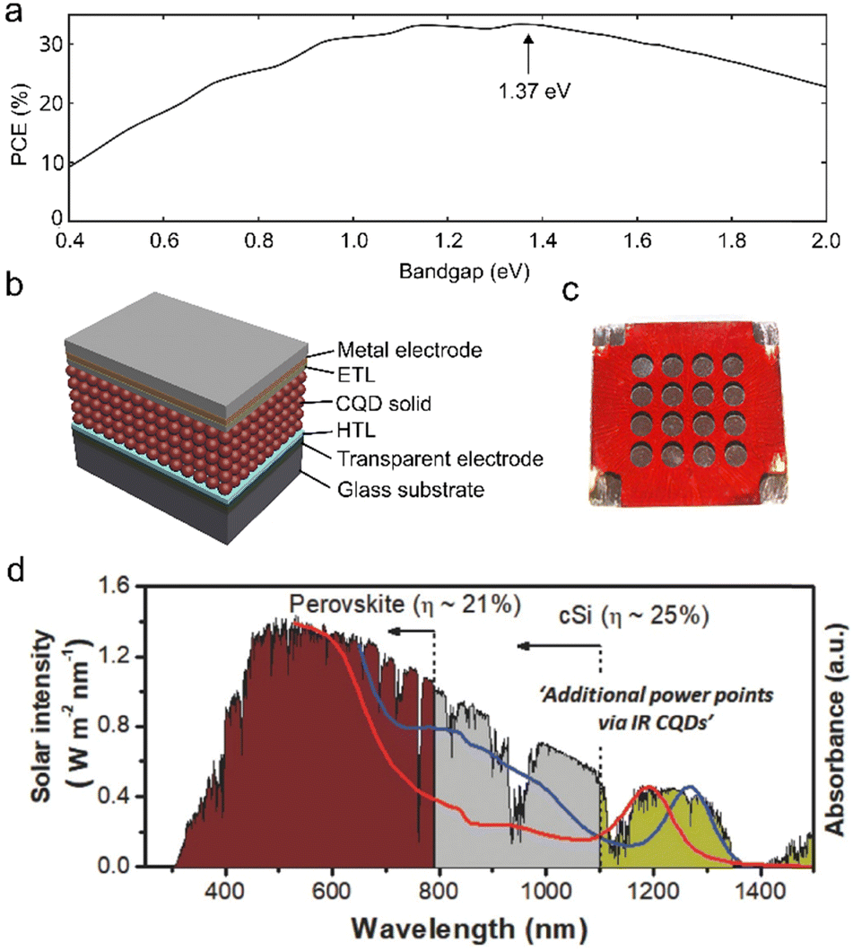 | ||
| Fig. 1 (a) Shockley–Queisser limit: PCE vs. bandgap.19 (b) Typical structure of a single-junction QDSC. Adapted with permission from ref. 20. Copyright 2015, John Wiley & Sons, Inc. (c) Photograph of a PbS QDSC. Reprinted from ref. 21 with CC BY-SA 3.0 license https://creativecommons.org/licenses/by-sa/3.0/ accessed on July 28th, 2023. (d) Solar spectrum and NIR CQD absorption. Reprinted with permission from ref. 22. Copyright 2015, John Wiley & Sons, Inc. | ||
The earliest applications of NIR CQDs in photovoltaics are either incorporating CQDs with wide bandgap materials to make dye-sensitized solar cells23,24 or blending CQDs with other semiconductors like organic photovoltaics.25 In 2005, Maria et al. reported an NIR QDSC based on the junction between PbS CQD solid and P3OT, an organic semiconductor.26 The National Renewable Energy Laboratory reported PbSe and PbS QDSCs in 200827 and 2010,28 with the PbS QDSC based on a heterojunction between PbS CQD solid and ZnO nanocrystal solid reaching a power conversion efficiency (PCE) of 3% (certified). Ma et al. reported a Schottky-junction QDSC based on ternary PbSxSe1−x CQDs, and the champion device reached a PCE of 3.3%.29
A typical structure of single-junction QDSCs can be seen from Fig. 1b and c. The device is normally comprised of several essential building blocks: the CQD solid as the light absorber, electron transport layer (ETL), hole transport layer (HTL), and electrodes (metals and transparent conductive oxides). Many strategies to enhance the PCE of single-junction lead chalcogenide QDSCs have been developed. The Sargent group has been focused on the surface chemistry of PbS CQDs. Halide atomic ligand exchange,30,31 methylammonium iodide ligand exchange,32 and phase-transfer ligand exchange (CQD ink with PbX2 (X = Br and I))33,34 have all been utilized to create more suitable PbS CQD solids for higher PCE. Different device architectures have also been developed to increase the PCE, including the gradient doping structure35 and inverted structure.36,37 Besides all these efforts, engineering the ETL and HTL has also been proven to be an effective route to increase PCE in recent endeavors, and the highest among them has reached 14%.38
The absorption spectrum of CQDs can be easily tuned by altering the size of CQDs, which can be achieved by changing the injection temperature in synthesis. Thus, by setting the bandgap to 1.0 eV or less, the first excitonic peak of the CQD solid will be more than 1200 nm, which means that the solid will have strong absorption in the NIR region. In recent years, PbS CQDs have been back into the spotlight of the photovoltaic research community for their ability to absorb NIR light over the wavelength of 1100 nm, which corresponds to 15% of the AM 1.5 solar irradiance.39 This makes it a perfect complement to silicon solar cells and perovskite solar cells, as shown in Fig. 1d. By harvesting NIR over 1100 nm, it can be added to the PCE of Si solar cells. Moreover, as a solution-processed polycrystalline material, CQD thin films can be mass-manufactured by different low-cost printing technologies, like blade printing,40 spray printing,41 and ink-jet printing.42 These technologies are suitable to be integrated into the current state-of-the-art solar cell manufacturing process, which enables the feasibility of large-scale manufacture of Si/CQD or perovskite/CQD tandem solar cells.
In 2015, Ip et al. demonstrated a multi-junction PbS QDSC with the first excitonic peak at ∼1200 nm.43 By utilizing a novel electron transport layer of PEIE, the device reached a full-spectrum PCE of 7.3%. To verify the feasibility of the QDSC, extra filters made of Si (cut-off wavelength: 1100 nm) and perovskite (cut-off wavelength: 750 nm) were utilized to acquire the values of PCE with radiation of specific NIR bands. The values of PCE with Si and perovskite filters are 0.8% and 2.8%, respectively, and the I–V curves of those devices are shown in Fig. 2a.
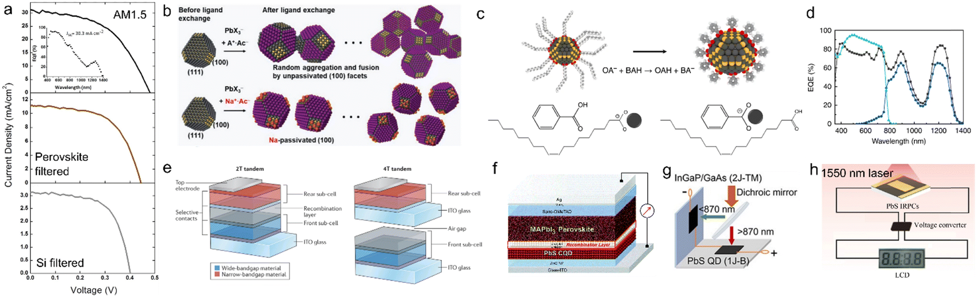 | ||
| Fig. 2 (a) I–V curves of a single-junction PbS CQD NIR solar cell under different conditions: AM 1.5, perovskite filtered, and Si filtered. Adapted with permission from ref. 43. Copyright 2015, American Chemical Society. (b) Illustration of passivating the (100) facets on PbS CQDs by Na+. Reprinted with permission from ref. 44. Copyright 2019 John Wiley & Sons, Inc. (c) Illustration of BA ligand exchange on PbS CQDs. Reprinted from ref. 45 with CC BY 4.0 license https://creativecommons.org/licenses/by/4.0/ (d) EQE results of devices with PbS-BA (amber) and PbS-EDT (navy) HTLs. Note: the cyan data points are the EQE of a perovskite solar cell. Reprinted from ref. 45 with CC BY 4.0 license https://creativecommons.org/licenses/by/4.0/ (e): Illustration of a 2T tandem solar cell and 4T tandem solar cell. Reprinted with permission from ref. 46. Copyright 2021 from Springer Nature Publishing Group. (f) Illustration of a perovskite/PbS CQD tandem solar cell. Reprinted with permission from ref. 47. Copyright 2018 from the Royal Society of Chemistry. (g) Illustration of spectral splitting solar cells by an InGaP/GaAs two-junction subcell and an NIR PbS quantum dot/ZnO nanowire subcell. Reprinted with permission from ref. 48. Copyright 2018 from American Chemical Society. (h) Illustration of an LCD screen powered by an NIR PbS QDSC harvesting a 1550 nm laser. Adapted with permission from ref. 49. Copyright 2023 from Springer Nature Publishing Group. | ||
The biggest difference between early single-junction PbS QDSCs and NIR PbS QDSCs for future tandem integration is the size of the CQDs. CQD solids with longer first-excitonic wavelengths consist of larger-sized CQDs, which contain a large portion of nonpolar (100) facets. However, the (100) facets were generally believed not to be passivated by commonly used atomic halide ligands. In 2019, Kim et al. developed a new strategy in phase-transfer ligand exchange to passivate the (100) facets.44 They utilized sodium acetate (NaAc) in the phase-transfer ligand exchange process, and the Na+ would passivate the (100) facets (Fig. 2b). The device possessed PCE of 8.1% under AM 1.5 and 0.9% with a Si filter. Liu et al. then employed ammonium formate in the ligand exchange process and reached a Si-filtered PCE of 0.96%.39 Besides the surface chemistry of CQDs, many other strategies have also been developed for increasing the PCE in the NIR region. Sun et al. mixed small-Eg CQDs with large-Eg CQDs to create a different absorber for higher Voc and achieved PCE of 0.94% with a Si filter.50 Choi et al.51 and Ge et al.52 developed more suitable components for NIR QDSCs, AZO ETL, and IHO transparent electrodes. Kim et al.,22 Liu et al.,53 and Baek et al.54 focused on the NIR QDSC structure. They developed a gradient doping structure, optimized the absorber thickness specifically for NIR, and patterned the HTL as a reflector. In 2020, Lee et al. developed an orthogonal colloidal quantum dot ink, PbS-BA (benzoic acid), to create the HTL (Fig. 2c),45 which will minimize the damage to the main absorber layer during HTL deposition. As a result, there is a significant increase in external quantum efficiency in the PbS-BA device (Fig. 2d), and the Si-filtered PCE reached 1.43%, which is the highest so far. The milestone works on single-junction NIR solar cells optimized for NIR absorption are listed in Table 1.
| Type | First-excitonic peak (nm) | PCE (AM 1.5) | PCE (perovskite filter) | PCE (Si filter) | Ref. |
|---|---|---|---|---|---|
| MoO3/PbS/PEIE/TiO2 | 1300 | 7.3% | 2.8% | 0.8% | 43 |
| PbS/ZnO | 1180 | 8.1% | NA | 0.9% | 44 |
| PbS-EDT/PbS-ink/ZnO | 1100 | 7.2% | NA | 0.96% | 39 |
| PbS-EDT/PbS-ink/ZnO | 1150 + 1520 | 8.5% | NA | 0.94% | 50 |
| PbS-EDT/PbS-ink/CAZO | 1200 | 8.35% | NA | 0.99% | 51 |
| PbS-EDT/PbS-ink/ZnO | 1300 | 11.15% | NA | 1.25% | 52 |
| PbS-EDT/Gradient PbS/ZnO | 1240 | 9.5% | 3.9% | 1.0% | 22 |
| PbS-EDT/PbS-ink/ZnO | 1270 | 9.5% | NA | 1.3% | 53 |
| MoO3/PBDTTT-E-T/PbS-ink/ZnO | 1188 | NA | NA | 1.34% | 54 |
| PbS-BA/PbS-ink/ZnO | ∼1230 | 8.87% | 3.57% | 1.43% | 45 |
As a result, tandem solar cells integrating NIR CQDs with Si, perovskite, and other visible light absorbers have been demonstrated. The integration strategies can be generally divided into the two-terminal (2T) route and the four-terminal (4T) route (Fig. 2e). A 2T tandem cell is the monolithic integration of two solar cells, while a 4T tandem cell is the mechanical integration of two cells. 4T devices are relatively easier to integrate (no recombination layer involved), but they normally include more wiring and transparent electrodes, which are not ideal for commercial applications.55 In 2018, Karani et al. demonstrated a prototype of a 2T perovskite/PbS CQD tandem cell.56 In the following years, by employing a recombination layer consisting of SnO2 and n-PEDOT, Zhang et al. reported a 2T perovskite/PbS CQD tandem device with PCE over 11%.47 Manekkathodi et al. then demonstrated a 4T perovskite/PbS CQD tandem cell, which achieved a PCE of 20.2% (Fig. 2f).57 Tavakoli et al. developed a new recombination layer of CuPC/Au/MoO3/ITO for the perovskite/PbS CQD tandem cell and reached an impressive PCE of 17.1% in 2T configuration and 21.1% in 4T configuration.58 The PCE of 4T devices is similar to that of the previous report,57 while the PCE in 2T significantly increases by employing the new recombination layer. In the previously mentioned work,45 Lee et al. also demonstrated a 4T perovskite/PbS CQD tandem solar cell by utilizing a semi-transparent perovskite solar cell, which has reached PCE of 22.07%.
QDSCs have also been integrated into solar cells other than perovskite solar cells. Kim et al. combined QDSC with the organic solar cell, resulting in a 2T organic/PbS CQD tandem solar cell with a PCE of 13.7%.59 Crisp et al.60 and Kern et al.61 have developed CdTe/PbS CQD and Sb2S3/PbS CQD tandem solar cells and the PCE values of their devices have reached 4.7% and 5.64%, respectively. The PCE of the 2T Sb2S3/PbS CQD tandem solar cell presented by Kern et al. has surpassed those of the control devices (Sb2S3 and PbS CQD single junction devices). This achievement strongly proves the feasibility of the designed device architecture and configuration, including the recombination layer. Besides all these experimental endeavours, a theoretical study of an a-Si/PbS CQD tandem solar cell has also been investigated, elucidating a 12% efficiency.62 The milestone works on tandem solar cells with QDSCs are listed in Table 2 shown below.
In recent years, novel applications of NIR QDSCs have also been developed. Because of the development in epitaxial lift-off technology, the cost of two-junction III–V compound solar cells has been significantly lowered.63 Consequently, Wang et al. demonstrated spectral splitting solar cells by InGaP/GaAs two-junction subcells and NIR PbS quantum dot/ZnO nanowire subcells (Fig. 2g).48 Using a dichroic mirror, NIR with wavelengths over 870 nm is transmitted onto the PbS CQD subcell (bottom of the mirror) and other wavelengths onto the InGaP/GaAs subcell (side of the mirror). The PbS CQD subcells were designed in a ZnO/PbS-TBAI/PbS-EDT architecture, and the main absorbing layer, PbS-TBAI, is with the first-excitonic peak at 1550 nm. The PbS CQD subcell reached a PCE of 2.44% after wavelength splitting. The whole cell's PCE was over 30% in both 2T and 4T configurations.
With the development of Internet-of-Things (IoT) technology and sensing technologies,64 wireless optical power transfer (WOPT) is gaining more attention with its ability to replace wiring in various working scenarios. Zhu et al. designed a PbS QDSC for utilization in WOPT.49 The CQD solid showed the first excitonic peak at an optical fiber communication wavelength of 1550 nm, and the device showed a promising PCE of over 10% with a 1550 nm laser. As shown in Fig. 2h, the PbS QDSC was able to drive an LCD screen by harvesting a 1550 nm laser.
3. CQD lasers and quantum light sources
Because of the extraordinary narrow-emission bandwidth, quantum dots have been widely applied in various semiconductor lasers.65 Most of these works utilized epitaxial quantum dots, differing from the easy and cost-effective production of CQDs. In recent years, CQDs have attracted tremendous attention in the laser research community. CQD holds unique properties like tunable emission and a nearly temperature-dependent gain threshold.8 Moreover, as CQD is a class of solution-processed materials, it is easier to integrate into the complementary metal–oxide–semiconductor (CMOS) fabrication process, which will enable low-cost on-chip laser source solutions. Current research on CQD laser mostly focuses on the visible spectrum,66e.g., CdSe CQD67 and perovskite CQD.68NIR laser is an essential ingredient in optical communication and many other industrial applications. However, as a bandgap tunable material, CQD has not been introduced into this field until recently. The main reason is that for the popular CQD NIR absorbers, such as the lead chalcogenide CQDs, the degeneracy at the band edge is as high as eight, which means that the multi-exciton process exists in lead chalcogenide CQDs. This property is favourable for photovoltaic applications but is uncomplimentary for lasing applications because the multi-exciton process will induce fast, non-radiative Auger recombination. The illustration of the biexciton Auger recombination is shown in Fig. 3a. It can be seen that instead of creating the stimulated emission, Auger recombination will transfer the energy to another charge carrier, which will cause a fast Auger decay to suppress the emission. Consequently, it will increase the optical gain threshold and shorten the optical gain lifetime. It is noteworthy that in bulk materials, because of the translational momentum conservation, the Auger decay rates are low.69 However, in CQDs, as the translational momentum conservation is relaxed, the fast Auger decay will suppress lasing uppress.70
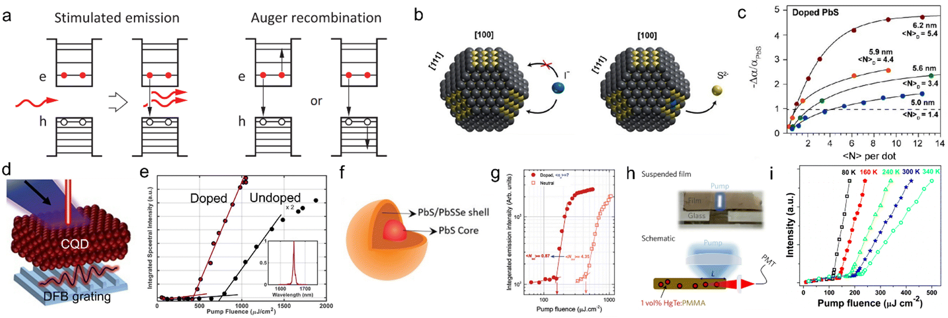 | ||
| Fig. 3 (a) Illustrations of the biexciton processes of stimulated emission and Auger recombination. Reprinted with permission from ref. 69 Copyright 2021, Springer Nature Publishing Group. (b) Illustration of selective doping on (100) facets on PbS CQDs by replacing S2− with I−. Reprinted with permission from ref. 71. Copyright 2020, American Chemical Society. (c) The gain comparison of differently sized PbS CQD solids with different doping schemes. Reprinted with permission from ref. 71. Copyright 2020, American Chemical Society. (d) Illustration of the first DFB CQD laser. Adapted with permission from ref. 72. Copyright 2021, Springer Nature Publishing Group. (e) Comparison of optically pumped lasing characteristics of DFB CQD lasers with doped CQD solid and undoped CQD solid. Adapted with permission from ref. 72. Copyright 2021 Springer Nature Publishing Group. (f) Illustration of a core–shell structure PbS CQD. Reprinted with permission from ref. 73. Copyright 2023 John Wiley & Sons, Inc. (g) Optically pumped lasing characteristics of doped and undoped core–shell PbS CQD DFB lasers. Reprinted with permission from ref. 73. Copyright 2023, John Wiley & Sons, Inc. (h) Schematic of the HgTe/PMMA laser and optically pumped lasing setup. Reprinted with permission from ref. 74. Copyright 2023, Nature Publishing Group. (i) Optically pumped lasing characteristics of Ag2Se CQD lasers with different temperatures. Reprinted with permission from ref. 75. Copyright 2022, the Royal Society of Chemistry. | ||
Despite the theoretical facts, some early works still managed to demonstrate amplified spontaneous emission in the NIR band with lead chalcogenide CQDs76–78 with some acceptable figure-of-merits because of the large absorption cross-section of lead chalcogenide CQDs.
To solve this problem, the Konstantatos Group concentrates on engineered PbS CQDs. Based on previous work on CdSe CQD,79 in 2020, they accomplished permanently heavily doped PbS CQDs by using iodide ions to replace the sulfide ions on the (100) surfaces of PbS CQDs (Fig. 3b). As a result, the doped electrons presenting on the conduction band will help reach the population inversion. By this mean, they successfully reached ASE with single-exciton gain and gain lifetime of 25–35 ps in PbS CQD films, and the lasing range can be tuned from 1530 nm to 1650 nm, covering the L-band and C-band.71 In 6.2 nm CQDs, single-exciton gain can be achieved as what can be seen in the transient absorption measurement in Fig. 3c. In a following-up work, Whitworth et al. integrated the aforementioned doped PbS CQD film with a distributed feedback (DFB) cavity, demonstrating a PbS CQD DFB laser (Fig. 3d).72 The lasing threshold of the DFB laser is 430 μJ cm−2 (Fig. 3e), while linewidths were as low as ∼0.9 meV. Taghipour et al. further optimized the PbS CQD lasing film by mixing CQDs with ZnO nanocrystals80 and developing a core–shell structure of PbS/PbSSe CQDs (Fig. 3f).73 The ZnO nanocrystals embedded in the PbS CQD solid will remotely passivate the in-gap states to suppress the Auger recombination, enabling a lasing threshold as low as 385 μJ cm−2. The core–shell structure will heavily suppress the Auger process.81 By combining the core–shell structure with the previously mentioned heavily doped PbS CQDs, the gain threshold is lowered to sub-single-exciton level and the measured lasing threshold is 300 μJ cm−2. The gain increased to an amazing value of 2180 cm−1 (Fig. 3g), which is the highest of the current state-of-the-art CQD NIR lasers. Optically pumped amplified spontaneous emission in PbS CQD film was also observed in an electrically driven device, which can be a promising approach for future NIR laser diodes.82 Besides conventional PbS CQD solids, PbS-CQD doped glass was also developed, and optical amplification has been observed.83 This solution can be potentially used in optical-fiber lasers.
Other investigations on this topic utilized materials other than lead chalcogenide to go around the problem of Auger recombination caused by the eightfold degeneracy. Geiregat et al. employed HgTe CQDs embedded in a PMMA matrix (Fig. 3h) and reached a lasing threshold of 40 mW cm−2 in continuous waves.74 Ag2Se CQD is another good candidate. Liao et al. observed amplified spontaneous emission in an Ag2Se CQD film, and the lasing threshold is as low as ∼200 μJ cm−2,75 which shows great potential in future lasing applications. In this work, the temperature-dependent lasing characterization was performed (Fig. 3i). At 80 K, the lasing threshold is 114 μJ cm−2, which verified the point that the gain threshold of the CQD laser is insensitive to temperature. The milestone works on NIR CQD lasers are listed in Table 3.
| Type | Temperature | ASE wavelengths | Pump | Threshold | Gain | Ref. |
|---|---|---|---|---|---|---|
| PbSe CQD (film) | Cryogenic | 1550 nm | 800 nm (pulsed) | ∼2 mW | ∼100 cm−1 | 76 |
| PbS CQD (film) | RT | ∼1300 nm | 800 nm (pulsed) | 1 mJ cm−2 | 260 cm−1 | 77 |
| PbS CQD (capillary) | Cryogenic | 1532 nm | 800 nm (pulsed) | 177 μJ cm−2 | NA | 78 |
| PbS CQD (film) | RT | 1530 nm | 800 nm (pulsed) | 70 μJ cm−2 | ∼110 cm−1 | 71 |
| PbS CQD (DFB) | RT | 1650 nm | 1030 nm (pulsed) | 430 μJ cm−2 | ∼100 cm−1 | 72 |
| PbS CQD (DFB) | RT | 1650 nm | 1030 nm (pulsed) | ∼385 μJ cm−2 | NA | 80 |
| PbS core–shell CQD (DFB) | RT | 1670 nm | 1030 nm (pulsed) | 300 μJ cm−2 | 2180 cm−1 | 73 |
| HgTe CQD (in PMMA) | RT | ∼1500 nm | 1028 nm (CW) | 50 mW cm−2 | 100–500 cm−1 | 74 |
| Ag2Se CQD (film) | Cryogenic & RT | 1312 nm | 800 nm (pulsed) | 114 (80 K) & 200 (RT) μJ cm−2 | NA | 75 |
Unlike lasers, which are coherent light sources, quantum light sources emit anti-bunched photons down to one single photon. They are essential devices for quantum information technologies. As ‘artificial atoms’, quantum dots are instinctive for this application because the discrete energy levels allow emission of single photons or multiple entangled photons. Over the past decades, epitaxial quantum dots have been widely exploited in single-photon sources.84 In recent years, various CQD-based single-photon sources have been developed for quantum light sources, such as CdSe CQDs85 and perovskite CQDs.86,87 However, research on NIR CQD quantum light sources is still not sufficient. In 2016, Nozaka et al. realized single NIR photon emission by a single PbS CQD coupled in a Si cavity.88 In 2017, Xie et al. utilized an antenna fabricated on fiber to detect NIR single-photon emission from PbS CQDs in a PMMA matrix.89 But till now, there has still been no systematic work on quantum light characterization, such as degree of coherence characterization.
4. CQD photodetectors
Photodetectors utilize the photoelectric effect, in which photons with sufficient energy higher than the bandgap of the semiconductor material hit the material surface and excite electrons, which are then free to move under an internal or externally applied electric field and form a photocurrent. Photodetectors are among the most ubiquitous devices nowadays and cover almost all the optical spectrum. The largest volume of applications is from image and video cameras, high dynamic range (HDR) cameras in our cell phones, fast-speed and high-resolution cameras for live broadcasts, palm-size digital cameras to dashcams installed on automobiles, etc. Charge-coupled devices (CCD) have dominated the imaging market for decades since their invention in the 1960s, as they provide HDR, high accuracy, and high image qualities. Advanced by complementary-metal–oxide semiconductor (CMOS) technology, CMOS cameras have taken over the market, as the technology offers a smaller footprint, lower cost, and power consumption with much faster speed compared to CCD cameras, while CCD cameras are only used in high-end demanding applications, such as space telescope and medical equipment, due to the high accuracy and greater HDR.Silicon, the most mature material utilized in the modern integrated circuit (IC) industry, is widely employed as the absorbing material inside photodetectors as well as imaging cameras. However, due to its weak absorption in IR spectral regions, other bulk materials are therefore introduced, such as germanium, indium gallium arsenide (InGaAs), lead sulfide (PbS), etc. On the other hand, benefiting from the high absorption, tunable bandgap through crystal size control, low-cost synthesis, and solution processing, CQD materials have emerged as alternative candidates for photodetection. In the IR range, especially that beyond Si absorption (>1000 nm), CQD photodetectors have raised tremendous attention. While various CQD materials have been exploited for the application, main materials, including lead (PbX, X stands for S, Se, Te), mercury chalcogenide (HgX, X stands for S, Se, Te), and III–V CQDs have stood out among the others. In the NIR range, PbS CQDs have emerged as the most mature technology, thanks to the low trap density and superior stability. While most other CQDs photodetectors are exploited for the mid-IR range, their applications in NIR will also be briefly discussed here.
In this section, we will revisit the early studies on CQD photodetectors, which mainly focus on increasing device efficiency, sensitivity, and speed through device structure design and material innovations. We do notice that, in recent years, the focus has been shifted towards improving the CQD ink stability and forming arrays of photodetectors when integrated with backplane platforms such as CMOS read-out integrated circuits (ROICs) to enable low-cost image sensors. With ink stability continuing to improve, large-area film homogeneity will also be enhanced, which is crucial for large-area integration of CQDs with ROICs and achieving higher manufacturing yields, especially at wafer levels. We will also discuss other platforms with which CQDs could potentially seek to integrate, such as Si photonics.
The configurations for CQD-based photodetectors are categorized into three types (Fig. 4): photoconductor, photodiode, and phototransistor. Comparison of milestone works with these three device configurations are summarized in Table 4.
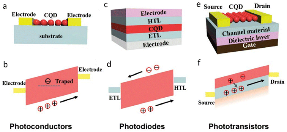 | ||
| Fig. 4 Configurations of previously demonstrated CQD NIR photodetectors and their energy band diagrams. (a) and (b) Photoconductor, (c) and (d) photodiode, and (e) and (f) phototransistor. Reprinted with permission from ref. 9. Copyright 2020, John Wiley & Sons, Inc. | ||
| Structure | Rise/fall time | Detectivity [Jones] | EQE | Responsivity [A W−1] | Voltage bias | Ref. |
|---|---|---|---|---|---|---|
| Photoconductor | NA | 1.8 × 10¹³@1300 nm | NA | >103 | 40 V | 90 |
| Photoconductor | NA | 3.2 × 10¹⁰@1400 nm | NA | <0.1 | 10 V | 91 |
| Photoconductor | 400 ns–2 μs | 1 × 10⁹@1400 nm | NA | 30 | 60 V | 92 |
| Phototransistor | 10–12 μs | 2.1 × 10¹⁰@1000 nm | NA | 0.18 | V DS = 5 V; VGS = 1 V | 93 |
| Phototransistor | ≤42 ms | 3 × 10¹¹@940 nm | NA | 1.58 | 10 V | 94 |
| Phototransistor | 10 ms | 7 × 10¹³@950 nm | NA | 5 × 10⁷ | V DS = 5 V | 95 |
| Phototransistor | ≤12 ms | 2.2 × 10¹²@980 nm | 28%@VG = 0 | 600 | V G = −15 V | 96 |
| Phototransistor | 0.95 to 1 ms | 5 × 10⁹ to 1 × 10¹¹@850 nm | NA | 5 × 10⁴ to 2 × 10² | V GS = 60 V to VGS = −40 V | 97 |
| Phototransistor | sub-ms | 1 × 10¹³@1600 nm | 14% | 4 × 10⁷ | V TD = 0.3 V | 98 |
| Photodiode | 300 ns | 1 × 10¹²@1450 nm | 25% | NA | −1 V | 99 |
| Photodiode | 4.6 to 8 μs | 1.1 × 10¹²@1000 nm, −1.5 V | 5% to 20% | NA | 0 to −1.5 V | 100 |
| Photodiode | 9.5 to 7 μs | 1.1 × 10¹²@1130 nm, −1 V | 24%@−1 V |
|
0 to −3 V | 101 |
| Photodiode | 318 μs | 7.98 × 10¹¹@890 nm, −7 V | 15–183% | 1.31@−7 V | 0 to −7 V | 102 |
| Photodiode | 160 μs | 2.26 × 10¹¹@930 nm, −3 V | 10% to 166% | 1.24@−3 V | −1 V to −4 V | 103 |
| Photodiode | 3 to 8 ms | 5 × 10¹¹ to 7 × 10¹³@1200 nm | 10% to 18700% | NA | −4 V to −12 V | 104 |
| Photodiode | 0.8 to 47.6 μs | 2.94 × 10¹¹@1490 nm | 12.7% | 0.153 | −0.25 V | 105 |
| Photodiode | 1.2 to 1.9 μs | 3.2 × 10¹¹ to 8 × 10¹⁰@128 0nm | 35% to 44% | Around 0.1 | −1 V to −4 V | 106 |
| Photodiode | 50 μs | 4.73 × 10¹³ to 1.92 × 10¹³@1550 nm | NA | 125 to 410 | −0.4 V to −1.5 V | 107 |
Photoconductor
A photoconductor features the most straightforward device structure among the others. Its name suggests that the device will be more electrically conducting under light illumination because the light illumination excites electrons, which increases the number of carriers in the conducting channel, leading to reduced channel resistance. Photoconductor possesses gains, and the widely accepted gain mechanism is that generated photocarriers under illumination circulate multiple times in the device before recombination, which is equivalent to creating multiple times more photocarriers. Thus, the gain (G) in a photoconductor can be approximated aswhere τrlt and τtt are recombination lifetime (or carrier lifetime) and transit time, L is the channel length, μ is carrier mobility, and Vi and Vbias are the built-in and external bias voltages, respectively. The equation is an estimation, and it is more complicated in practice. For instance, electric fields will rarely be evenly distributed across channels, and mobility values for electrons and holes are rarely the same. Detailed analyses of these scenarios are outside the scope of this review. In many photoconductors based upon materials such as gallium arsenide (GaAs), nanowires and other 2-dimensional (2D) materials, non-ideal states situated in the device localize minority carriers, which may increase τrlt of minority carriers and finally leads to further increase of photoconductive gain. In a CQD-based photoconductor, the photo-gain is also enhanced by large number of trap states associated with CQDs, leading to ‘trap-assisted’ gain. With light illumination, excess majority carriers circulate inside the channel through metal contacts while minority carriers are localized inside trap states until they escape and recombine. As such, these trap states act like trapping centers that prolong minority carrier lifetimes. In contrast, others argue the classical theory to be imprecise and even misleading.108 They argue a photoconductor intrinsically exhibits no high gain, while experimentally observed high photo-gain in the photoconductor is induced by extrinsic effects, such as non-ideal surface states that localize minority carriers, creating an excess number of majority carriers, which change channel conductivity and increase the photo-gain. Nevertheless, both theories reach a consensus that photo-gain in the photoconductor is associated with non-ideal states in the devices.
Very early studies on CQD photodetectors mostly exploited photoconductor structures. The first published attempt of CQD photodetector was demonstrated by Wang and Herron in 1992 using cadmium sulfide (CdS) with the photoconductor structure.109 Because the CQD exhibits near-insulating properties, the authors utilized a hole-transporting polymer as a carrier-transporting medium and doped it with the cadmium sulfide (CdS) CQD, which served as sensitizer centers for photogeneration. Other Cd-based CQDs were also investigated, such as cadmium solenoid (CdSe) and cadmium tellurium (CdTe).110–112 Later studies were focused on exploring photoconductors using pure CQD solids, with devices demonstrated both in lateral and sandwich structures,113,114 which were, however, challenged by the extremely poor photocurrents and thus low efficiencies due to the near-insulating colloids. The challenge was finally addressed in 2003 when a strategy, what now is the so-called ‘solid–ligand exchange’ protocol, was proposed to replace long native and insulating ligands with shorter and more conductive ones, e.g., dithiols or diamines.115
The first NIR CQD photodetector was demonstrated by Sargent and co-workers in 2004 with the photoconductor structure. The photoconductor was based on a PbS-CQD/polymer composite. Although the internal quantum efficiency was extremely low (∼10−5), the study was the first to showcase the possibility of CQD for a plethora of NIR photodetection applications.116 Later in 2006, with the help of solid-state ligand-exchange and short ligand of n-butylamine (length ∼0.6 nm), the same group made a breakthrough and demonstrated an ultrasensitive NIR photoconductor using pure PbS-CQD solids, with a responsivity greater than 1000 A W−1 and specific detectivity up to 1.8 × 10¹³ Jones at 1300 nm and a voltage bias of 40 V (Fig. 5a). The high photo-gain is closely associated with the in-gap trap state.90 It has been shown that the in-gap trap states close to the mid of PbS CQD bandgap are formed during solid-state ligand exchange, which could significantly prolong τrlt and therefore, increase photo-gain.117–119 These in-gap states were also shown to play a dominant role in carrier transport in the dark,118 which inevitably increases dark current. Photoconductors consisting of other CQD materials are mainly for longer IR wavelengths, although some NIR applications have been demonstrated. Heiss’ group demonstrated the first HgTe CQD photoconductor using the inkjet-printing technique and showed a responsivity less than 0.1 A W−1 at a voltage bias of 10 V at 1.4 μm. The efficiency gradually increases with decreasing illumination power, showing a non-linear response in the intensity range, which is induced by trap states in the device91 (Fig. 5b). The low efficiency is mainly due to the low-mobility CQDs arising from their long organic ligand (dodecanenthiol). Photoconductors made with short thiol-capped HgTe CQDs showed a slight increase in the responsivity (0.4 A W−1) at 60 V bias at a wavelength of 1.4 μm and low illumination intensity. Under sufficiently high illumination intensity (∼0.8 W cm−2), the device exhibited a 3 dB bandwidth higher than 1 MHz (1 kHz @ 0.8 mW cm−2) but much reduced responsivity (0.02 A W−1)92 (Fig. 5c). This intensity-dependent behavior is universal for the photodetectors based on the trap-assisted gain mechanism manifest the extremely important role of in-gap states for photodetector performances. In such devices, with increasing illumination intensity, more in-gap states are occupied, which leads to a higher biomolecular recombination rate and shorter carrier lifetime. While a shorter carrier lifetime leads to lower gain, it does expedite photodetector responses.
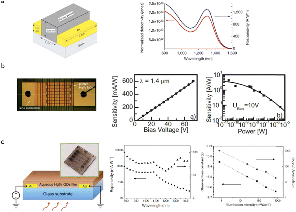 | ||
| Fig. 5 (a) Device structure of the ultrasensitive NIR photoconductor using pure PbS-CQD solids, and the responsivity and normalized detectivity spectra. Reprinted with permission from ref. 90. Copyright 2006, Springer Nature Limited. (b) Top view of the inkjet-printed nanocrystal photodetector, and its bias dependence and illumination power dependence of sensitivity at 1.4 μm. Reprinted with permission from ref. 91. Copyright 2007, John Wiley & Sons, Inc. (c) Device structure of the aqueous HgTe CQD based photoconductors; responsivity and IQE as a function of wavelength, and the change of the temporal response and the responsivity with different illumination levels. Reprinted with permission from ref. 92. Copyright 2014, John Wiley & Sons, Inc. | ||
Nonetheless, photoconductor devices based upon HgTe exhibit lower efficiency and sensitivity values (typical specific detectivity of lower than the order of 1010 Jones) compared to PbS counterparts (up to the order of 1013 Jones), mainly due to their larger number of trap states associated with the material.
The interest in CQD photoconductor studies rapidly faded away, which was when CQD phototransistor studies gained momentum. Since a phototransistor essentially has more control over the channel with one more terminal, CQD phototransistors quickly became the platform, which is highly versatile for studying CQD material science and device structure innovation.
The application scenarios of photoconductors mostly fall into two major categories. First, due to their ease of fabrication, they show up in applications where sensitivity is not required but cost is highly valued, e.g., low-wave infrared detection. Second, their simple architecture avoids photon absorption from other materials. Therefore, they are extensively exploited in UV and X-ray imaging, where signals from visible light should be excluded.
Phototransistors
Compared to photoconductor devices, phototransistors have three terminals, which offer much better control over channel CQD materials. By applying gate voltages in addition to source and drain biases, the carrier concentration, and thus, channel conductivity will vary. This provides chances for the studies of material sciences. Nagpal and Klimov utilized such a structure to study the role of in-gap states for the charge transport and photoconductivity of CQD films.118 By applying a more negatively biased gate voltage, two new spectral peaks were observed at 0.9 eV and 1.5 eV for CQDs with a bandgap of Eg = 1.3 eV. The new peaks were found to be associated with the optical transitions between quantized valence bands (1S and X) and the in-gap states (Fig. 6a). The peaks were more prominent with greater negative gate voltage because, at such voltage, the in-gap states were less occupied and more optical transitions occur. Such gating effects were absent with pristine CQD films, which suggested the in-gap states were likely introduced during the ligand-exchange step. It was also concluded that these in-gap states formed weakly conducting pathways, which were responsible for charge transport under dark while under illumination, photocurrents were dominated by hole transport at the valence band edge (Fig. 6a). In 2015, Zhang et al., for the first time, demonstrated the images of the conducting pathway induced by the in-gap states using Kelvin probe force microscopy and confirmed that under dark, electrons percolate via the pathway while holes percolate via the valence band (Fig. 6b).120 These in-gap states could be, however, detrimental to device performances. For instance, open-circuit voltage in CQD solar cells will be determined by the in-gap states and always be lower than the ideal value for a given bandgap (Eg). For photodetector devices, while under illumination, gain could be enhanced owing to prolonged carrier lifetime, and the dark current sees an inevitable increase induced by the in-gap states and device response will be slowed down by long carrier lifetimes. One solution to mediate this is by adding electron donors, which provide electrons that passivate in-gap states and thus effectively reduce dark current and improve device speed (Fig. 6c).121 Another way to circumvent the problem has been proposed by Adinolfi et al. By adding a layer of molybdenum trioxide (MoO3) atop the CQD channel layer, a heterojunction is formed between the two materials, which fully depletes the channel and effectively suppresses the dark current. The built-in electric field also expedites charge carrier escape from the trap states, reducing minority carrier lifetimes. Therefore, the gain is reduced while the device speed is increased (Fig. 6d). The MoO3 layer modulates the device uppress just like the gate does in conventional phototransistors.93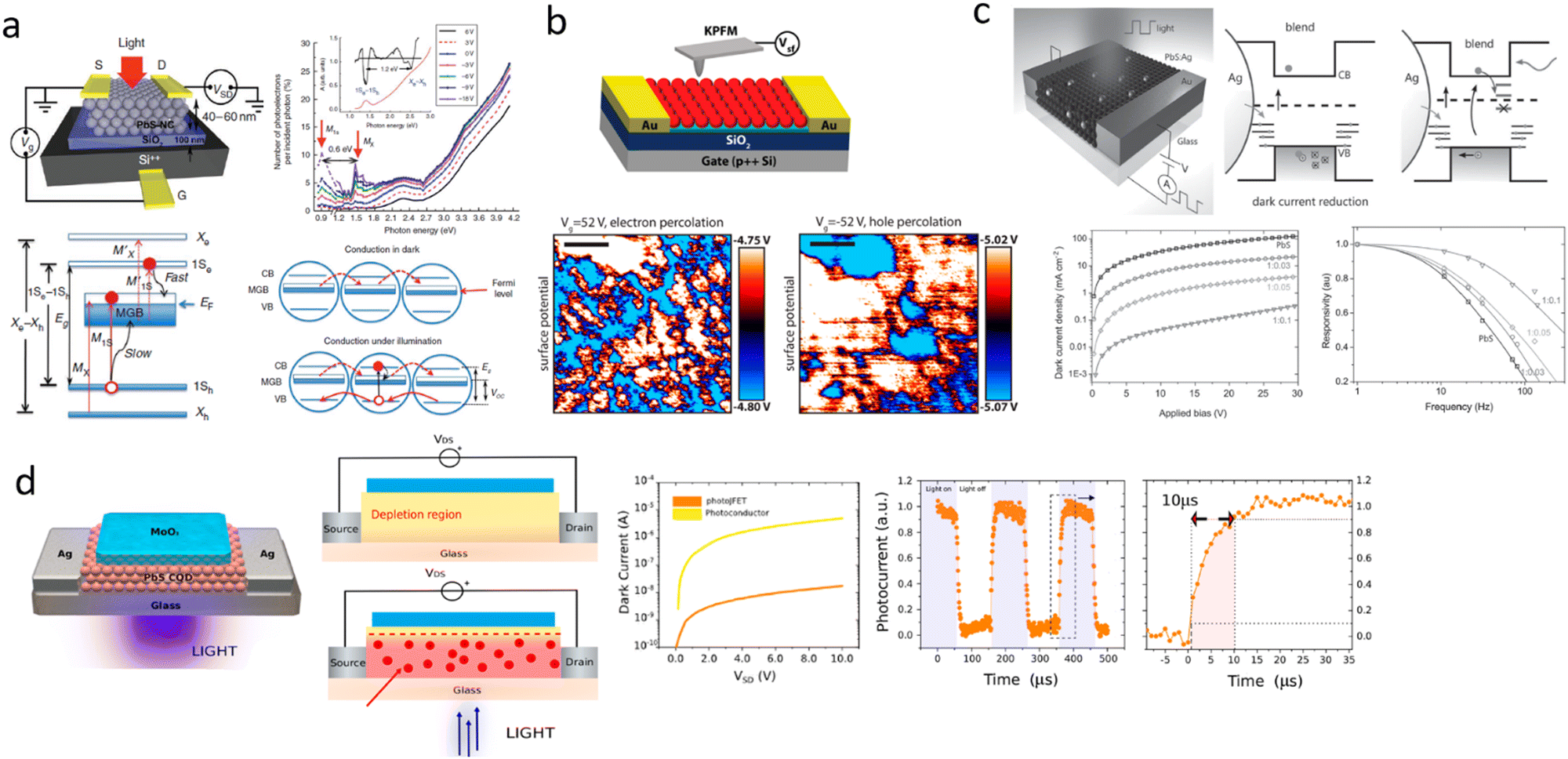 | ||
| Fig. 6 (a) Device structure of PbS–NC OFETs; photocurrent as a function of incident photon energy shown in terms of the number of photoelectrons per 100 incident photons (new peaks at 0.9 eV and 1.5 eV were found); energy level diagram and conduction mechanisms in dark and under illumination. Reprinted with permission from ref. 118. Copyright 2011, Springer Nature Limited. (b) Device structure of a CQD thin film FET and KPFM probe setup, and surface potential maps at Vg = 52 V and Vg = −52 V. Reprinted with permission from ref. 120. Copyright 2015, American Chemical Society. (c) Device structure of PbS:Ag photoconductor; mechanism responsible for the dark current reduction; dark current density–applied voltage trends for different PbS QD:Ag NP combination; responsivity as a function of frequency for different PbS QD:Ag NP combination. Reprinted with permission from ref. 121. Copyright 2015, John Wiley & Sons, Inc. (d) Device structure of the photoJFET with MoO3 layer. The fully depleted device exhibited reduces carriers, whereas illumination generates large number of free carriers. Comparison of dark current between the photoJEFT and a pure CQD photoconductor. The speed characterization of the photoJFET. Reprinted with permission from ref. 93. Copyright 2015 American Chemical Society. | ||
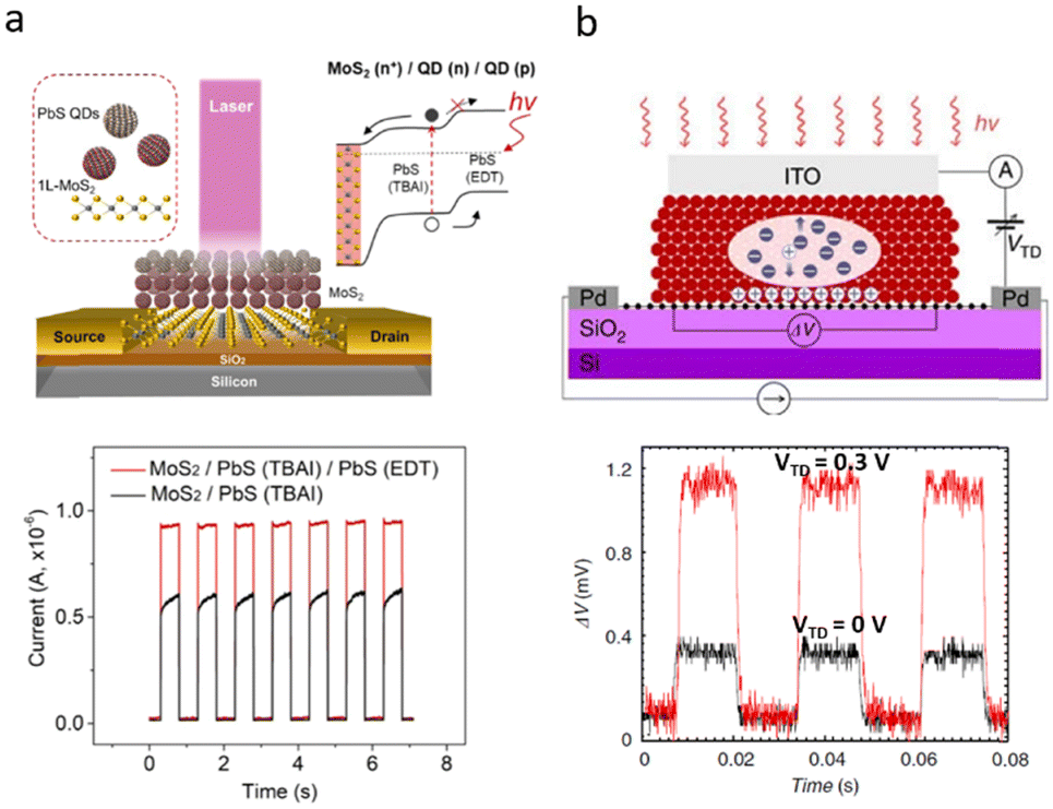
CQDs normally exhibit low carrier mobility, and this leads to limited gain. Extensive studies have been demonstrated to integrate CQDs with high-mobility materials, forming a hybrid phototransistor structure and exhibiting superior photo gain. CQDs have been successfully combined with MAPbI3 perovskite,94 various 2D materials, including graphene,95 Bi2O2Se nanosheets122 and transition metal dichalcogenide (TMD) materials such as MoS2 and WS296,123 (Fig. 7). In the hybrid structure, high-absorption CQDs serve as the sensitizing gate while high-mobility materials are applied as the conducting channel. The CQDs gate and channel form a built-in field with which, under light, photocarriers generated in the CQD layer will transit to the channel and then circulate in the channel repeatedly. One deficiency is the relatively low speed due to the slow separation process of photocarriers inside the CQD layer. To this end, some have demonstrated the integration of CQD junctions as a photo-gate, and the strong built-in field inside the CQD layer swiftly separates the generated photocarriers97,98,124 (Fig. 8). Several reports have provided a thorough review of hybrid phototransistors, in which detailed discussions and comparisons of device working mechanisms and performances are also given.9,125
 | ||
| Fig. 7 CQDs combined with (a) a MAPbI3 perovskite and the corresponding responsivity and detectivity spectra on light wavelength. Reprinted with permission from ref. 94. Copyright 2019 American Chemical Society. (b) Graphene and its spectral responsivity of two phototransistors of single and bilayer graphene with PbS CQDs. Reprinted with permission from ref. 95. Copyright 2012, Springer Nature Limited. (c) Bi2O2Se nanosheets and the photoresponse spectra. Reprinted with permission from.122 Copyright 2019, American Chemical Society. (d) and (e) MoS2 and the corresponding responsivity as a function of wavelength. Reprinted with permission from ref. 123 Copyright 2014, John Wiley & Sons, Inc. Adapted with permission from ref. 96. Copyright 2016, American Chemical Society. | ||
 | ||
| Fig. 8 (a) Device structure of the MoS2/PbS QD hybrid phototransistor and its temporal response traces. Reprinted with permission from ref. 97. Copyright 2022, American Chemical Society. (b) Device structure of the hybrid graphene-CQD phototransistor and its temporal response traces. Reprinted with permission from ref. 98. Copyright 2016, Springer Nature Limited. | ||
Because phototransistors are able to effectively regulate the signal, they mostly appear in applications for weak signal detection.
Photodiodes
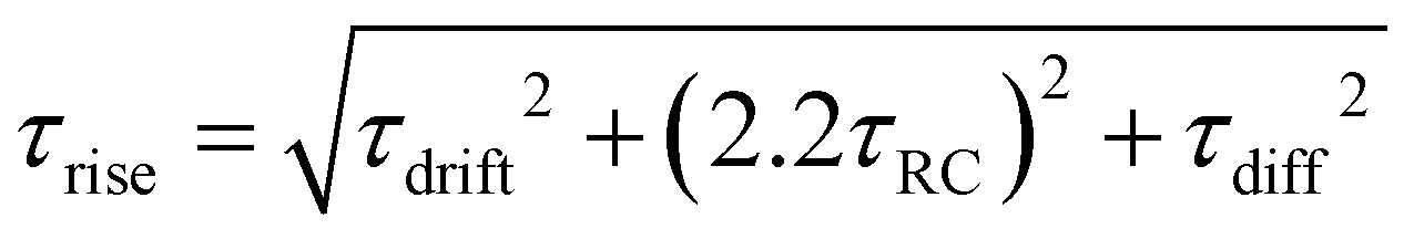
CQD photodiodes exhibit built-in electric field, which could be generated from the Schottky junctions between CQDs and metal electrodes, or the p–n homojunctions within CQDs, or the heterojunctions between CQDs and heavily doped electron/hole transport layers and/or other semiconductor materials. Compared to the trap-assist gain mechanism discussed in CQD photoconductor and phototransistor structures, the working mechanism in a CQD photodiode is based on charge separation under an electric field; therefore, conventional photodiodes work under zero or reverse voltage bias and offer no gain but the fastest speed and lowest dark current. In addition, for a photodetector, photocurrent (Iph) scales with light intensity (P) as Iph ∼ Pk, where k ≤ 1 is an empirical number that decreases when carrier trapping and emission from trap states dominate the devices. When k decreases, photocurrent will be less linear with light intensity. Most reported CQD photodiodes show k values close to 1. Photodetector speed is characterized by rise time (τrise) and 3 dB bandwidth (f3dB). Rise time in a photodiode is given byτdrift is the transit time taken by photocarriers to quickly travel in the depletion region under the built-in and externally applied electric field. τRC is the resistor–capacitor (RC) time constant required by the output signal to exponentially increase to 1 − e−1 or fall to e−1 of its peak steady-state value; for this exponential increase/fall to reach 90%/10%, a multiplier factor of 2.2 must be added. τdiff is the diffusion time required by photocarriers in the neutral region to slowly diffuse to the electrodes or depletion region before being swept by the electric field. From the equation, to have the highest speed possible, it is desirable to eliminate the diffusion process and have a fully depleted photodiode.
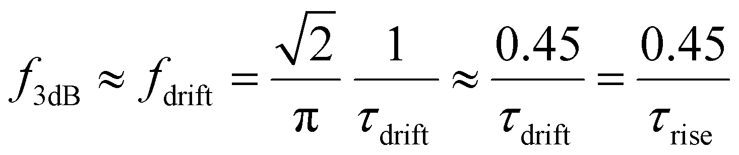
Further, f3dB is correlated with the τrise. When the photodetector speed is limited by carrier drift time (τrise ≈ τdrift)
Advances in CQD photodiodes have been reviewed in detail elsewhere,9,126,127 and here we will focus on the main milestones. Schottky junction photodiodes are constructed using suitable metals, e.g., Au for n-type and Al for p-type CQDs. Clifford et al. presented the first CQD Schottky photodiode, in which a Schottky junction is formed between the p-type PbS CQD and Al electrode, whereas an ohmic contact is formed between ITO and the CQD. 3 dB bandwidths of 1.5 MHz and 3 MHz at reverse biases of −0.5 V and −5 V were achieved, respectively (Fig. 9a).99 This was done by reducing the CQD layer thickness to be equal to the width of the depletion region, and thus, the photocarrier transport is solely based on drift. However, due to the weak built-in field, the depletion width and thus, the thickness of the active layer is only 180 nm. The over-thin active layer leads to inadequate light absorption and low efficiency. Additionally, the thin active layer, combined with the lack of hole-blocking layer and trap states existing at the Al/CQD interface, induces a large dark leakage current (>1 μA cm−2@−0.5 V) (Fig. 9a). Nevertheless, the device speed yielded by the Schottky photodiode structure was among the fastest for many years. Pal et al. improved dark current by adding a hole blocking layer of zinc oxide (ZnO), which extends the depletion region width and thus effectively uppress dark current (25 nA cm−2@−0.5 V)100 (Fig. 9b). By adding an extra layer of electron blocking layer of nickel oxide (NiO), Manders et al. managed to further reduce dark current to be lower than 20 nA cm−2@−0.5 V101 (Fig. 9c).
 | ||
| Fig. 9 (a) A schematic of the PbS CQD photodiode, frequency dependence (3 dB) on bias, and steady-state I–V characteristics in the dark and at 17.9 μW cm−2 illumination at 1550 nm. Reprinted with permission from ref. 99. Copyright 2008, Springer Nature Limited. (b) Device structure of ITO/PEDOT:PSS/PbS-NQD/ZnO/Al photodiode; its energy band diagram and the I–V characteristics in dark and under 200 μW cm−2 illumination at 500 nm. Reprinted with permission from.100 Copyright 2012, John Wiley & Sons, Inc. (c) Device structure of the PbS CQD photodetector with NiO electron blocking layer; its energy band diagram and dark current density on bias. Reprinted with permission from ref. 101. Copyright 2014 John Wiley & Sons, Inc. | ||
Among the other CQD materials, mercury chalcogenide CQDs exhibit the highest spectral tunability. While they are widely used for MIR, some NIR photodetectors have been demonstrated, and one typical example is the HgTe photodetector. HgTe CQDs are easily synthesized and have a widely tunable bandgap, having the potential to be applied in photodetectors in SWIR, MWIR, and even LWIR range. For example, Chen et al. recently reported a universal homojunction HgTe CQD infrared photodetector. This HgTe photodetector achieved a high detectivity of 1011 to 1012 Jones and EQE near 90% at the wavelength range of 1.5 to 3.6 μm.128 InAs CQD material is also attractive due to its non-toxicity.129,130 InAs CQDs have a very narrow band gap in the bulk form, which gives them the tunable sensing range. Moreover, the low dielectric constant of InAs CQDs films potentially allows for faster response times in photodetectors.
CQD photodiodes with high gain could also be achieved by introducing trap states in the device. This converts the gain mechanism from charge separation in a conventional CQD photodiode to trap-assisted gain, which is exploited in the CQD photoconductor and phototransistor but comes at the expense of deteriorated dark current and device speed. Shen et al. introduced a NIR, visible-blind CQD photodiode without any filter, which is done by fabricating a thick active layer (4 μm) and generated holes will not make it to the other side of the Ag electrode.102 PbS CQDs as sensitizing centers were mixed with PDTP-DFBT and PCBM as electron and hole transporting matrixes, and the hole trapping effect from the CQDs induced electron injection from the cathode. As a result, an EQE exceeding 100% (∼180%) was achieved at −7 V. Such high voltage bias is mainly due to the over-thick active layer. Because of the trap-assisted gain, a moderate dark current of 0.6 μA cm−2 and a slow response time of 318 μs were obtained (Fig. 10a). Another similar work was done by the same group, in which ZnO nanoparticles with a large number of electron trap states were introduced into the CQD:PCBM:P3HT blend, triggering hole injections from the anode.100 As such, EQE exceeding 1000% and 150% at −4 V were achieved in visible and NIR regions, respectively, but with a large dark current of 10 μA cm−2 at −4 V and a sluggish rise time of 160 μs (Fig. 10b). So's group presented a p–i–n CQD photodiode, in which ZnO and TPAC polymer served as hole and electron blocking layers.103 Instead of introducing trap states in the active layer, the TAPC layer was distorted with trap states. These non-ideal states were induced by Ag atoms that penetrated into the TAPC layer during the thermal evaporation process for the top Ag electrode deposition. A high EQE of 18![[thin space (1/6-em)]](https://www.rsc.org/images/entities/char_2009.gif) 700% at −13 V was achieved at the expense of a high dark current of 40 μA cm−2 at −13 V and a slow fall time of 8 ms as the photocarriers need to slowly detrap from the trap states (Fig. 10c).
700% at −13 V was achieved at the expense of a high dark current of 40 μA cm−2 at −13 V and a slow fall time of 8 ms as the photocarriers need to slowly detrap from the trap states (Fig. 10c).
 | ||
| Fig. 10 (a) Device structure of the nanocomposite photodetectors; the energy diagram of the photodetectors under illumination without and with PbS CQD traps; EQE spectra with PbS CQDs, and dark current and photocurrent curves with PbS CQDs. Reprinted with permission from ref. 102. Copyright 2016, the Royal Society of Chemistry. (b) Device structure of the dual-quantum dot hybrid photodetector; the energy band diagram under illumination and reverse bias; EQE spectra of the device under reverse bias; photo- and dark-current density–voltage curves of P3HT:PCBM, PbS:P3HT:PCBM and PbS:P3HT:PCBM:ZnO devices. Reprinted with permission from ref. 103. Copyright 2014, John Wiley & Sons, Inc. (c) Device structure of a gain PbS QD photodiode; energy band diagram under illumination; EQE spectra as function of wavelength under different reverse bias; I–V curves under dark and under illumination intensities of 165 μW cm−2. Reprinted with permission from ref. 104. Copyright 2015, John Wiley & Sons, Inc. | ||
Photodiodes hold extremely fast responses. Thus, they are widely employed in instantaneous imaging.
CQD inks for photodetectors
CQDs reviewed above are processed with solid-phase ligand exchange protocol. The CQD inks, which are passivated by lead halides through a solution-phase ligand exchange process, have produced the highest-quality photovoltaic devices by far. This phase-transfer exchange (PTE) method can provide lower defect concentrations, improved carrier transport, and better control over the film morphology of the CQDs; This one-step spin-coating also enables large-scale manufacturing. Niu et al. first introduced halogen ion ligands to PTE CQDs.131 CQDs with a larger size present the appealing potential of capturing photons in the IR range. However, as the size of the CQD increases, utilizing the PTE method for ink synthesis becomes challenging. This is because an increasing number of non-polar (100) facets become exposed with the increase in CQD size; however, lead halides can only passivate (111) facets effectively. To address this problem, Kim et al. introduced Na+ cations into the lead halide system, which can selectively passivate (100) facets44 (Fig. 2b). This approach ensured protection from CQD aggregation during the ligand exchange process and improved the performance of photovoltaic devices. Fan et al. presented a mixed lead halide (including PbI2, PbBr2 and PbCl2) ligand exchange method132 (Fig. 11a). Each lead halide is allowed to attach onto the most attritive facets, leading to enhanced passivation and higher carrier transport. The mixed lead halide PbS CQDs photovoltaic devices exhibited 90% IQE across the entire solar spectrum and 81% EQE in the infrared range. Furthermore, Choi et al. demonstrated a cascade surface modification method that can provide mastery over doping and solubility, facilitating both n-type and p-type CQD inks that seamlessly mix in the same solvent while ensuring complete surface passivation133 (Fig. 11b). Additionally, InAs CQD ink130 and HgTe CQD ink128 are also highly attractive to fabricate high-quality optoelectronic devices. | ||
| Fig. 11 (a) Lead halide exchange from an oleate capped PbS CQD to a halide-capped PbS CQD. Reprinted with permission from ref. 132. Copyright 2019, John Wiley & Sons, Inc. (b) Ligand exchange with lead halide anions and lead halide anions re-exchange with the functional ligands to render a p-type character process. Reprinted with permission from ref. 33. Copyright 2020, Springer Nature Limited. | ||
CQD integration with Si
Integrating Si CQDs effectively extends its spectral response into the IR range, while utilizing a Si-based platform opens a plethora of applications for CQDs. Masala et al. demonstrated a CQD photodetector in which CQDs were integrated with c-Si via a CQD:Si heterojunction and showcased the first heterojunction photodetector that exhibited appreciable EQEs in the NIR region.134 Building a high-quality heterojunction between Si and CQDs is a persistent challenge. Ning's group inserted a thin passivating ZnO layer between Si and PbS CQDs, resulting in a lower carrier recombination rate at the interface.105 The photodetector with a 10 nm ZnO layer showed a detectivity of 4.08 × 10¹¹ Jones at 1490 nm and response time up to microsecond scale (Fig. 12a). Top of form, thanks to the passivation of Si surface by two-step chlorination/methylation treatment method demonstrated by Xu et al.135 and the high-quality PbS CQDs ink passivated by lead halides as discussed in the previous content, a highly efficient c-Si:PbS CQD heterojunction photodiode was achieved by Xu et al.106 In this photodiode structure, the ZnO layer served as the electron transfer/hole blocking layer, and EDT-PbS CQDs layer served as the buffer layer to reduce interface carrier recombination and facilitate charge collection. The proposed heterojunction photodiode exhibited a detectivity of up to 2.58 × 10¹¹ Jones at −1 V bias voltage, an EQE up to 44% at −2 V bias voltage, and an ultrafast response time less than 4 μs (Fig. 12b). Zhou et al. presented a p-Si:PbS CQDs NIR photodetector with a photovoltage triode structure.107 When light is introduced, carriers generated in the CQD layer are separated by the built-in field. Photoelectrons transferred to the n-CQD region are temporarily localized at the p-Si:n-CQD boundary, which causes a negative photovoltage in the n-CQD region. Consequently, holes in silicon are pulled by this photovoltage and move to the CQDs region. This photodetector achieved both low dark current of 10−9 A cm−2 at 0 V bias voltage and ultra-high detectivity of 4.73 × 10¹³ Jones at 1550 nm and −0.4 V bias voltage (Fig. 12c). Recently, driven by the need of NIR imaging for applications such as autonomous driving, CQDs have been integrated with Si-ROICs to realize imager sensors. Researchers have extensively studied PbS CQDs based imagers that sense in the NIR range, as well as HgTe CQDs in the NIR and deeper in the MIR regime. The imagers could be achieved by integrating the CQD photodiode, pinned photodiode136 or photoconductor with Si-ROICs,137 or by forming a CQD/Si heterojunction.138 Pejovic et al. presented a PbS:Si-ROICs SWIR image sensor with a 3T pixel design, which achieved a 768 × 512-pixel array, 5 μm pixel pitch, and an EQE of 40% at 1450 nm.139 STMicroelectronics announced an NIR and SWIR image sensor with PbS CQDs thin film, which achieved pixel sizes down to 1.62 μm and a high EQE of 60% at 1400 nm.140 Emberion demonstrated an imager using a combination of PbS CQDs and graphene with 640 × 512 array size, which can operate in the 400–2000 nm range and achieved 20 μm pixel size and around 20% EQE at 1550 nm.141 Recently, a HgTe CQD imager was reported by Tang's group, which has a large format 1280 × 1024 pixel arrays and a pixel pitch of 15 μm. This imager exhibited 14% EQE with a cut-off wavelength of around 2 μm.142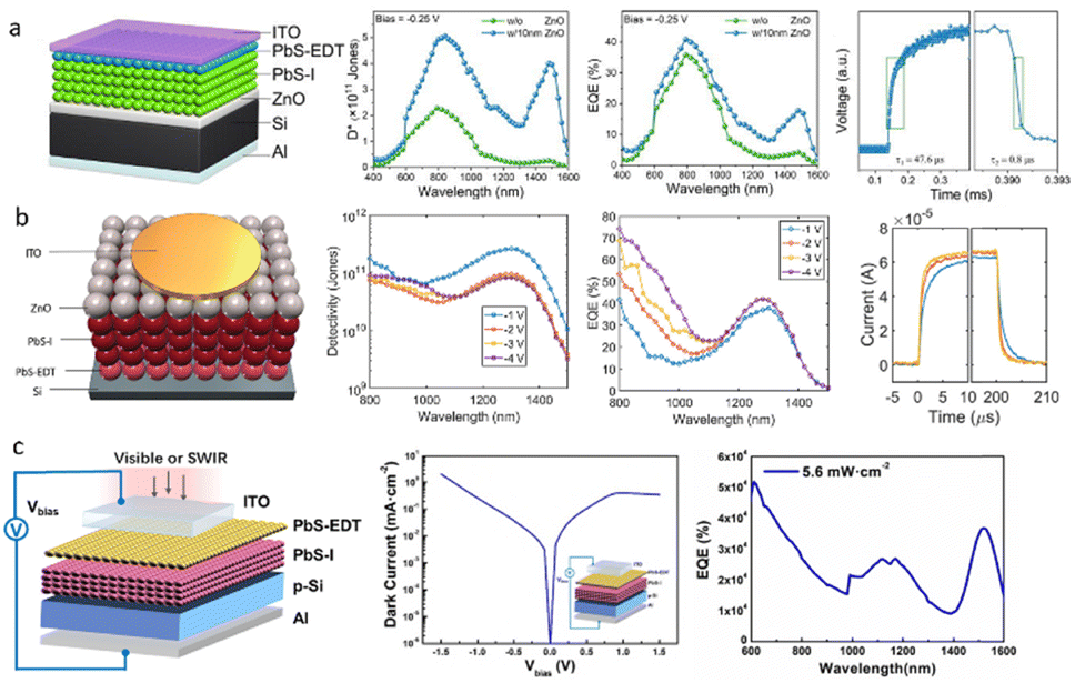 | ||
| Fig. 12 (a) Schematic of the structure of a Si:CQD photodiode with a 10 nm ZnO layer; detectivity spectra as function of wavelength; EQE spectra of the PD with and without ZnO layer; response time spectra. Reprinted with permission from ref. 105. Copyright 2020, AIP Publishing. (b) Device structure of a c-Si:PbS CQD heterojunction photodiode; detectivity spectra as function of wavelength under different bias; EQE spectra under different spectra; and response time spectra. Reprinted with permission from ref. 106. Copyright 2022, American Chemical Society. (c) Device structure of the p-Si:PbS CQDs photodetector; dark current curve; the spectral EQE plot. Reprinted with permission from ref. 107. Copyright 2021, Springer Nature Limited. | ||
5. Other applications
Since NIR technologies have broad applications in health, inspection, surveillance, etc., CQD optoelectronic devices have been integrated into research fields more closely aligned with engineering applications. In this section, two specific applications, wearable CQD optoelectronic devices and CQD biomedical devices, will be discussed.Wearable NIR CQD optoelectronic devices
Photoplethysmography (PPG) is a widely adopted technique to monitor physiological signals in current wearable electronic devices, exemplified by smartwatches. Within this context, CQDs have been identified as a promising candidate for wearable PPG devices. Beyond their exceptional NIR sensing capabilities, CQDs exhibit additional intriguing properties that entice researchers in this domain. As a class of polycrystalline materials, CQDs confer the capacity for deformation, a highly desirable trait for wearable devices. The solution processability of CQDs also makes them suitable for roll-to-roll (R2R) mass production for wearable devices.In 2014, Gao et al. reported a PPG heart rate detector employing a photoconductor using PbS CQD/carbon nanotube composite with PMMA encapsulation. Clear systole, diastole, and reflection are captured by the device.143 Subsequently, by introducing PI into the CQD suspension, Liang et al. optimized the morphology of the resulting PbS CQD thin film for better flexibility. They achieved a hetero-junction with the PbS CQD thin film on a flexible substrate, resulting in a wearable PPG device that can retrieve accurate PPG signals.144 Furthermore, other NIR CQDs have also been utilized to retract PPG signals, e.g., Cu–In–Se (CISe) CQD. In 2022, Li et al. developed a wearable PPG sensor based on hetero-junctions featuring a CISe CQD thin film.145
Expanding beyond wearable single CQD photodetectors, wearable CQD photodetectors (e.g., PbS CQD146) have also been designed to cater to a broader range of applications, including multispectral imaging, which can be applied in a variety of fields (machine vision, health imaging, artificial intelligence, etc.). In 2016, Tang et al. developed a flexible HgTe CQD photoconductor pixel array with different HgTe CQDs possessing different absorption features.147 In 2023, Liu et al. introduced a wearable imager based on a PbS CQD photodiode array capable of sensing photons from X-ray to NIR.148 PbS CQD has also found applications in wearable PV devices to power wearable healthcare devices.149 Remarkably, the device reached a PCE of 10.05% at AM 1.5 condition.
It is noteworthy that other wearable devices such as gas sensor,150 touch sensor151 and antibiotic surfaces have also been developed. However, because the primary focus of this article is on optoelectronic devices, they will not be discussed here.
NIR CQD biomedical devices
Due to their exceptional photoluminescence capability in the NIR band, NIR CQDs have been widely employed as biomarkers in biomedical imaging.152,153 Since the biomarkers are mostly free-standing CQDs, which are not on the device level, we will not extend the discussion here.Another interesting biomedical application that has emerged recently is the CQD optoelectronic biointerface. Novel bio-interface technologies have emerged in recent years.154 In 2022, Karatum et al. demonstrated a biointerface based on the PbS CQD heterojunction. With NIR activation, due to the photoelectric effect, electrical stimulation will be generated on the device to stimulate neurons.155
6. Conclusions and prospects
Since the first set of reports on CQDs for solar cells, NIR lasers and NIR photodetectors in the 1990s and 2000s, those fields have gone through rapid development in the past two decades. CQD single-junction solar cells have reached 14% efficiency, and multi-junction solar cells using CQDs as NIR absorbers have achieved above 22% efficiency. Optically pumped NIR lasers using CQDs have been demonstrated, although electrically pumped lasers are preferred for practical applications. Finally, CQDs photodetectors have already been demonstrated using various device architectures. CQD materials have also been employed for the NIR imaging sensors.In the foreseeable future, there remain unexplored avenues within the realm of CQD optoelectronic devices and related research:
(1) System-level integration of CQD PV devices for IoT and wearable devices: CQD PV devices exhibit significant promise for future IoT and wearable devices. However, system-level integration with sensing and logic platforms is still lacking. In the future, there is a pressing need for extensive research in comprehensive platform-level integration solutions to harness the full potential of CQD PV devices in these applications.
(2) Advanced tandem CQD PV solutions: both 2T and 4T tandem CQD PV solutions need further exploration. The current PCE achieved in tandem PV devices utilizing CQD subcells falls short of their inherent potential. Future research endeavours can be focused on optimizing tandem PV devices by integrating CQDs with other materials, such as Si and perovskite thin films. This collaborative approach has the potential to significantly enhance the PCE of tandem PV systems.
(3) Electrically pumped CQD lasers and photonic integration: presently, CQD lasers predominantly rely on optical pumping. As the field progresses toward integrated photonics, there is a compelling need to develop electrically pumped CQD lasers. Additionally, there is a critical need to explore the integration of CQD lasers with passive photonic components and even active photonic components. Such integration efforts can open up new possibilities in future optical interconnection, biosensing platforms, LiDAR, etc.
(4) CQDs integrated into the Si platform will bring NIR imaging sensors to new markets like LiDAR ranging and AR/VR. CQD-based single-photon avalanche diode (SPAD) using the Si platform has a huge potential for quantum information.
In the next decade, innovation and originality to improve CQD materials and engineer CQD device structures will foster the development of CQD optoelectronics.
Conflicts of interest
There are no conflicts to declare.Acknowledgements
The authors appreciate funding support from the Natural Sciences and Engineering Research Council of Canada.Notes and references
- W. E. Buhro and V. L. Colvin, Nat. Mater., 2003, 2, 138–139 CrossRef CAS PubMed.
- J. Jean, J. Xiao, R. Nick, N. Moody, M. Nasilowski, M. Bawendi and V. Bulović, Energy Environ. Sci., 2018, 11, 2295–2305 RSC.
- C. R. Kagan, E. Lifshitz, E. H. Sargent and D. V. Talapin, Science, 2016, 353, aac5523 CrossRef PubMed.
- M. Liu, N. Yazdani, M. Yarema, M. Jansen, V. Wood and E. H. Sargent, Nat. Electron., 2021, 4, 548–558 CrossRef.
- E. Jang and H. Jang, Chem. Rev., 2023, 123, 4663–4692 CrossRef CAS PubMed.
- Y.-M. Huang, K. J. Singh, A.-C. Liu, C.-C. Lin, Z. Chen, K. Wang, Y. Lin, Z. Liu, T. Wu and H.-C. Kuo, Nanomaterials, 2020, 10, 1327 CrossRef CAS PubMed.
- J. Kim, J. Roh, M. Park and C. Lee, Adv. Mater., 2023, 2212220 CrossRef PubMed.
- Y.-S. Park, J. Roh, B. T. Diroll, R. D. Schaller and V. I. Klimov, Nat. Rev. Mater., 2021, 6, 382–401 CrossRef CAS.
- K. Xu, W. Zhou and Z. Ning, Small, 2020, 16, 2003397 CrossRef CAS PubMed.
- G. H. Carey, A. L. Abdelhady, Z. Ning, S. M. Thon, O. M. Bakr and E. H. Sargent, Chem. Rev., 2015, 115, 12732–12763 CrossRef CAS PubMed.
- C. R. Kagan, L. C. Bassett, C. B. Murray and S. M. Thompson, Chem. Rev., 2020, 121, 3186–3233 CrossRef PubMed.
- R. Wang, Y. Shang, P. Kanjanaboos, W. Zhou, Z. Ning and E. H. Sargent, Energy Environ. Sci., 2016, 9, 1130–1143 RSC.
- J. Zhou, J. Zhu, W. He, Y. Cao, J. Pang, J. Ni and J. Zhang, J. Alloys Compd., 2023, 938, 168593 CrossRef CAS.
- I. P. Marko and S. J. Sweeney, IEEE J. Sel. Top. Quantum Electron., 2017, 23, 1–12 Search PubMed.
- Y. Cao, P. Qu, C. Wang, J. Zhou, M. Li, X. Yu, J. Pang, W. Zhou, H. Liu and G. Cuniberti, Adv. Opt. Mater., 2022, 10, 2200816 CrossRef CAS.
- L. Hu, Z. Yang, A. Mandelis, A. Melnikov, X. Lan, G. Walters, S. Hoogland and E. H. Sargent, J. Phys. Chem. C, 2016, 120, 14416–14427 CrossRef CAS.
- I. Ramiro, B. Kundu, M. Dalmases, O. Özdemir, M. Pedrosa and G. Konstantatos, ACS Nano, 2020, 14, 7161–7169 CrossRef CAS PubMed.
- Y. Zhu, G. Pan, L. Shao, G. Yang, X. Xu, J. Zhao and Y. Mao, J. Alloys Compd., 2020, 835, 155390 CrossRef CAS.
- https://www.mathworks.com/matlabcentral/fileexchange/43879-shockleyqueisser .
- M. Yuan, O. Voznyy, D. Zhitomirsky, P. Kanjanaboos and E. H. Sargent, Adv. Mater., 2015, 27, 917–921 CrossRef CAS PubMed.
- https://en.wikipedia.org/wiki/Quantum_dot_solar_cell#cite_note-1 .
- J. Kim, O. Ouellette, O. Voznyy, M. Wei, J. Choi, M.-J. Choi, J. W. Jo, S.-W. Baek, J. Fan and M. I. Saidaminov, et al. , Adv. Mater., 2018, 30, 1803830 CrossRef PubMed.
- P. Yu, K. Zhu, A. G. Norman, S. Ferrere, A. J. Frank and A. J. Nozik, J. Phys. Chem. B, 2006, 110, 25451–25454 CrossRef CAS PubMed.
- A. Zaban, O. Mićić, B. Gregg and A. Nozik, Langmuir, 1998, 14, 3153–3156 CrossRef CAS.
- S. A. McDonald, G. Konstantatos, S. Zhang, P. W. Cyr, E. J. Klem, L. Levina and E. H. Sargent, Nat. Mater., 2005, 4, 138–142 CrossRef CAS PubMed.
- A. Maria, P. W. Cyr, E. J. Klem, L. Levina and E. H. Sargent, Appl. Phys. Lett., 2005, 87, 213112 CrossRef.
- J. M. Luther, M. Law, M. C. Beard, Q. Song, M. O. Reese, R. J. Ellingson and A. J. Nozik, Nano Lett., 2008, 8, 3488–3492 CrossRef CAS PubMed.
- J. M. Luther, J. Gao, M. T. Lloyd, O. E. Semonin, M. C. Beard and A. J. Nozik, Adv. Mater., 2010, 22, 3704–3707 CrossRef CAS PubMed.
- W. Ma, J. M. Luther, H. Zheng, Y. Wu and A. P. Alivisatos, Nano Lett., 2009, 9, 1699–1703 CrossRef CAS PubMed.
- J. Tang, K. W. Kemp, S. Hoogland, K. S. Jeong, H. Liu, L. Levina, M. Furukawa, X. Wang, R. Debnath and D. Cha, et al. , Nat. Mater., 2011, 10, 765–771 CrossRef CAS PubMed.
- L. Meng and X. Wang, Energies, 2022, 15, 2458 CrossRef CAS.
- X. Lan, O. Voznyy, F. P. García de Arquer, M. Liu, J. Xu, A. H. Proppe, G. Walters, F. Fan, H. Tan and M. Liu, et al. , Nano Lett., 2016, 16, 4630–4634 CrossRef CAS PubMed.
- M. Liu, O. Voznyy, R. Sabatini, F. P. García de Arquer, R. Munir, A. H. Balawi, X. Lan, F. Fan, G. Walters and A. R. Kirmani, et al. , Nat. Mater., 2017, 16, 258–263 CrossRef CAS PubMed.
- J. Xu, O. Voznyy, M. Liu, A. R. Kirmani, G. Walters, R. Munir, M. Abdelsamie, A. H. Proppe, A. Sarkar and F. P. García de Arquer, et al. , Nat. Nanotechnol., 2018, 13, 456–462 CrossRef CAS PubMed.
- C.-H. M. Chuang, P. R. Brown, V. Bulović and M. G. Bawendi, Nat. Mater., 2014, 13, 796–801 CrossRef CAS PubMed.
- R. Wang, X. Wu, K. Xu, W. Zhou, Y. Shang, H. Tang, H. Chen and Z. Ning, Adv. Mater., 2018, 30, 1704882 CrossRef PubMed.
- L. Meng, Q. Xu, U. K. Thakur, L. Gong, H. Zeng, K. Shankar and X. Wang, ACS Appl. Mater. Interfaces, 2020, 12, 53942–53949 CrossRef CAS PubMed.
- H. I. Kim, S.-W. Baek, H. J. Cheon, S. U. Ryu, S. Lee, M.-J. Choi, K. Choi, M. Biondi, S. Hoogland and F. G. de Arquer, et al. , Adv. Mater., 2020, 32, 2004985 CrossRef CAS PubMed.
- M. Liu, F. Che, B. Sun, O. Voznyy, A. Proppe, R. Munir, M. Wei, R. Quintero-Bermudez, L. Hu and S. Hoogland, et al. , ACS Energy Lett., 2019, 4, 1225–1230 CrossRef CAS.
- N. Sukharevska, D. Bederak, V. M. Goossens, J. Momand, H. Duim, D. N. Dirin, M. V. Kovalenko, B. J. Kooi and M. A. Loi, ACS Appl. Mater. Interfaces, 2021, 13, 5195–5207 CrossRef CAS PubMed.
- I. J. Kramer, G. Moreno-Bautista, J. C. Minor, D. Kopilovic and E. H. Sargent, Appl. Phys. Lett., 2014, 105, 163902 CrossRef.
- G. Kara, S. Bolat, K. Sharma, M. J. Grotevent, D. N. Dirin, D. Bachmann, R. Furrer, L. F. Boesel, Y. E. Romanyuk and R. M. Rossi, et al. , Adv. Mater. Technol., 2023, 2201922 CrossRef CAS.
- A. H. Ip, A. Kiani, I. J. Kramer, O. Voznyy, H. F. Movahed, L. Levina, M. M. Adachi, S. Hoogland and E. H. Sargent, ACS Nano, 2015, 9, 8833–8842 CrossRef CAS PubMed.
- Y. Kim, F. Che, J. W. Jo, J. Choi, F. P. García de Arquer, O. Voznyy, B. Sun, J. Kim, M.-J. Choi and R. Quintero-Bermudez, et al. , Adv. Mater., 2019, 31, 1805580 CrossRef PubMed.
- S. Lee, M.-J. Choi, G. Sharma, M. Biondi, B. Chen, S.-W. Baek, A. M. Najarian, M. Vafaie, J. Wicks and L. K. Sagar, et al. , Nat. Commun., 2020, 11, 4814 CrossRef CAS PubMed.
- Y. J. Ahn, S. G. Ji and J. Y. Kim, J. Korean Ceram. Soc., 2021, 58, 399–413 CrossRef CAS.
- Y. Zhang, M. Gu, N. Li, Y. Xu, X. Ling, Y. Wang, S. Zhou, F. Li, F. Yang and K. Ji, et al. , J. Mater. Chem. A, 2018, 6, 24693–24701 RSC.
- H. Wang, S. Nakao, N. Miyashita, Y. Oteki, M. Giteau, Y. Okada, T. Takamoto, H. Saito, S. Magaino and K. Takagi, et al. , ACS Energy Lett., 2022, 7, 2477–2485 CrossRef CAS.
- M. Zhu, Y. Zhang, S. Lu, Z. Wang, J. Zhou, W. Ma, R. Zhu, G. Chen, J. Zhang and L. Gao, et al. , Front. Optoelectron., 2023, 16, 1–11 CrossRef PubMed.
- B. Sun, O. Ouellette, F. P. García de Arquer, O. Voznyy, Y. Kim, M. Wei, A. H. Proppe, M. I. Saidaminov, J. Xu and M. Liu, et al. , Nat. Commun., 2018, 9, 4003 CrossRef PubMed.
- J. Choi, J. W. Jo, F. P. G. de Arquer, Y.-B. Zhao, B. Sun, J. Kim, M.-J. Choi, S.-W. Baek, A. H. Proppe and A. Seifitokaldani, et al. , Adv. Mater., 2018, 30, 1801720 CrossRef PubMed.
- C. Ge, E. Yang, X. Zhao, C. Yuan, S. Li, C. Dong, Y. Ruan, L. Fu, Y. He and X. Zeng, et al. , Small, 2022, 18, 2203677 CrossRef CAS PubMed.
- S. Liu, M.-Y. Li, K. Xiong, J. Gao, X. Lan, D. Zhang, L. Gao, J. Zhang and J. Tang, Nano Res., 2023, 16, 2392–2398 CrossRef CAS.
- S.-W. Baek, P. Molet, M.-J. Choi, M. Biondi, O. Ouellette, J. Fan, S. Hoogland, F. P. García de Arquer, A. Mihi and E. H. Sargent, Adv. Mater., 2019, 31, 1901745 CrossRef PubMed.
- Z. Wang, Z. Song, Y. Yan, S. Liu and D. Yang, Adv. Sci., 2019, 6, 1801704 CrossRef PubMed.
- A. Karani, L. Yang, S. Bai, M. H. Futscher, H. J. Snaith, B. Ehrler, N. C. Greenham and D. Di, ACS Energy Lett., 2018, 3, 869–874 CrossRef CAS.
- A. Manekkathodi, B. Chen, J. Kim, S.-W. Baek, B. Scheffel, Y. Hou, O. Ouellette, M. I. Saidaminov, O. Voznyy and V. E. Madhavan, et al. , J. Mater. Chem. A, 2019, 7, 26020–26028 RSC.
- M. M. Tavakoli, H. T. Dastjerdi, P. Yadav, D. Prochowicz, H. Si and R. Tavakoli, Adv. Funct. Mater., 2021, 31, 2010623 CrossRef CAS.
- H. I. Kim, S.-W. Baek, M.-J. Choi, B. Chen, O. Ouellette, K. Choi, B. Scheffel, H. Choi, M. Biondi and S. Hoogland, et al. , Adv. Mater., 2020, 32, 2004657 CrossRef CAS PubMed.
- R. W. Crisp, G. F. Pach, J. M. Kurley, R. M. France, M. O. Reese, S. U. Nanayakkara, B. A. MacLeod, D. V. Talapin, M. C. Beard and J. M. Luther, Nano Lett., 2017, 17, 1020–1027 CrossRef CAS PubMed.
- S. Kern, G. Yi, P. Büttner, F. Scheler, M.-H. Tran, S. Korenko, K. E. Dehm, I. Kundrata, S. Albrecht, J. Bachmann and R. W. Crisp, Monolithic two-terminal tandem solar cells using Sb2S3 and solution-processed PbS quantum dots achieving an open-circuit potential beyond 1.1 V, ChemRxiv, 2023, preprint DOI:10.26434/chemrxiv-2023-f4k03.
- S. Kashyap, R. Pandey, J. Madan and R. Sharma, Phys. Status Solidi A, 2020, 217, 2000252 CrossRef CAS.
- R. Tatavarti, G. Hillier, G. Martin, A. Wibowo, R. Navaratnarajah, F. Tuminello, D. Hertkorn, M. Disabb, C. Youtsey, D. McCallum, et al., 2009 34th IEEE Photovoltaic Specialists Conference (PVSC), 2009, pp. 002065–002067 Search PubMed.
- Y. Li, S. Huang, S. Peng, H. Jia, J. Pang, B. Ibarlucea, C. Hou, Y. Cao, W. Zhou, H. Liu and G. Cuniberti, Small, 2023, 19, 2206126 CrossRef CAS PubMed.
- S. Pan, V. Cao, M. Liao, Y. Lu, Z. Liu, M. Tang, S. Chen, A. Seeds and H. Liu, J. Semiconductors, 2019, 40, 101302 CrossRef CAS.
- P. Geiregat, D. Van Thourhout and Z. Hens, NPG Asia Mater., 2019, 11, 41 CrossRef CAS.
- N. Ahn, C. Livache, V. Pinchetti, H. Jung, H. Jin, D. Hahm, Y.-S. Park and V. I. Klimov, Nature, 2023, 617, 79–85 CrossRef CAS PubMed.
- S. Yakunin, L. Protesescu, F. Krieg, M. I. Bodnarchuk, G. Nedelcu, M. Humer, G. De Luca, M. Fiebig, W. Heiss and M. V. Kovalenko, Nat. Commun., 2015, 6, 8056 CrossRef CAS PubMed.
- H. Jung, N. Ahn and V. I. Klimov, Nat. Photonics, 2021, 15, 643–655 CrossRef CAS.
- J. M. Pietryga, K. K. Zhuravlev, M. Whitehead, V. I. Klimov and R. D. Schaller, Phys. Rev. Lett., 2008, 101, 217401 CrossRef PubMed.
- S. Christodoulou, I. Ramiro, A. Othonos, A. Figueroba, M. Dalmases, O. Ozdemir, S. Pradhan, G. Itskos and G. Konstantatos, Nano Lett., 2020, 20, 5909–5915 CrossRef CAS PubMed.
- G. Whitworth, M. Dalmases, N. Taghipour and G. Konstantatos, Nat. Photonics, 2021, 15, 738–742 CrossRef CAS PubMed.
- N. Taghipour, M. Dalmases, G. L. Whitworth, M. Dosil, A. Othonos, S. Christodoulou, S. M. Liga and G. Konstantatos, Adv. Mater., 2023, 35, 2207678 CrossRef CAS PubMed.
- P. Geiregat, A. J. Houtepen, L. K. Sagar, I. Infante, F. Zapata, V. Grigel, G. Allan, C. Delerue, D. Van Thourhout and Z. Hens, Nat. Mater., 2018, 17, 35–42 CrossRef CAS PubMed.
- C. Liao, L. Tang, Y. Li, S. Sun, L. Wang, J. Xu, Y. Jia and Z. Gu, Nanoscale, 2022, 14, 10169–10175 RSC.
- R. Schaller, M. Petruska and V. Klimov, J. Phys. Chem. B, 2003, 107, 13765–13768 CrossRef CAS.
- V. Sukhovatkin, S. Musikhin, I. Gorelikov, S. Cauchi, L. Bakueva, E. Kumacheva and E. Sargent, Opt. Lett., 2005, 30, 171–173 CrossRef CAS PubMed.
- S. Hoogland, V. Sukhovatkin, I. Howard, S. Cauchi, L. Levina and E. Sargent, Opt. Express, 2006, 14, 3273–3281 CrossRef CAS PubMed.
- K. Wu, Y.-S. Park, J. Lim and V. I. Klimov, Nat. Nanotechnol., 2017, 12, 1140–1147 CrossRef CAS PubMed.
- N. Taghipour, G. L. Whitworth, A. Othonos, M. Dalmases, S. Pradhan, Y. Wang, G. Kumar and G. Konstantatos, Adv. Mater., 2022, 34, 2107532 CrossRef CAS PubMed.
- M. Nasilowski, P. Spinicelli, G. Patriarche and B. Dubertret, Nano Lett., 2015, 15, 3953–3958 CrossRef CAS PubMed.
- N. Taghipour, I. Tanriover, M. Dalmases, G. L. Whitworth, C. Graham, A. Saha, O. Özdemir, B. Kundu, V. Pruneri and K. Aydin, et al. , Adv. Funct. Mater., 2022, 32, 2200832 CrossRef CAS.
- D. Chen, B. Xu, Z. Fang, D. Zhang, T. Man, J. Mo, X. Liu, Z. Xu, Y. Liu and S. Cao, et al. , Adv. Photonics Res., 2022, 3, 2200097 CrossRef CAS.
- P. Senellart, G. Solomon and A. White, Nat. Nanotechnol., 2017, 12, 1026–1039 CrossRef CAS PubMed.
- X. Lin, X. Dai, C. Pu, Y. Deng, Y. Niu, L. Tong, W. Fang, Y. Jin and X. Peng, Nat. Commun., 2017, 8, 1132 CrossRef PubMed.
- G. Rainò, M. A. Becker, M. I. Bodnarchuk, R. F. Mahrt, M. V. Kovalenko and T. Stöferle, Nature, 2018, 563, 671–675 CrossRef PubMed.
- H. Utzat, W. Sun, A. E. Kaplan, F. Krieg, M. Ginterseder, B. Spokoyny, N. D. Klein, K. E. Shulenberger, C. F. Perkinson and M. V. Kovalenko, et al. , Science, 2019, 363, 1068–1072 CrossRef CAS PubMed.
- T. Nozaka and K. Mukai, Phys. E, 2016, 78, 14–18 CrossRef CAS.
- Z. Xie, Y. Lefier, M. A. Suarez, M. Mivelle, R. Salut, J.-M. Merolla and T. Grosjean, Nano Lett., 2017, 17, 2152–2158 CrossRef CAS PubMed.
- G. Konstantatos, I. Howard, A. Fischer, S. Hoogland, J. Clifford, E. Klem, L. Levina and E. H. Sargent, Nature, 2006, 442, 180–183 CrossRef CAS PubMed.
- M. Böberl, M. V. Kovalenko, S. Gamerith, E. J. W. List and W. Heiss, Adv. Mater., 2007, 19, 3574–3578 CrossRef.
- M. Chen, H. Yu, S. V. Kershaw, H. Xu, S. Gupta, F. Hetsch, A. L. Rogach and N. Zhao, Adv. Funct. Mater., 2013, 24, 53–59 CrossRef.
- V. Adinolfi, I. J. Kramer, A. J. Labelle, B. R. Sutherland, S. Hoogland and E. H. Sargent, ACS Nano, 2015, 9, 356–362 CrossRef CAS PubMed.
- J.-Y. Zhang, J.-L. Xu, T. Chen, X. Gao and S.-D. Wang, ACS Appl. Mater. Interfaces, 2019, 11, 44430–44437 CrossRef CAS PubMed.
- G. Konstantatos, M. Badioli, L. Gaudreau, J. Osmond, M. Bernechea, F. P. de Arquer, F. Gatti and F. H. Koppens, Nat. Nanotechnol., 2012, 7, 363–368 CrossRef CAS PubMed.
- D. Kufer, T. Lasanta, M. Bernechea, F. H. Koppens and G. Konstantatos, ACS Photonics, 2016, 3, 1324–1330 CrossRef CAS.
- S. Pak, Y. Cho, J. Hong, J. Lee, S. Lee, B. Hou, G.-H. An, Y.-W. Lee, J. E. Jang, H. Im, S. M. Morris, J. I. Sohn, S. Cha and J. M. Kim, ACS Appl. Mater. Interfaces, 2018, 10, 38264–38271 CrossRef CAS PubMed.
- I. Nikitskiy, S. Goossens, D. Kufer, T. Lasanta, G. Navickaite, F. H. Koppens and G. Konstantatos, Nat. Commun., 2016, 7, 11954 CrossRef CAS PubMed.
- J. P. Clifford, G. Konstantatos, K. W. Johnston, S. Hoogland, L. Levina and E. H. Sargent, Nat. Nanotechnol., 2008, 4, 40–44 CrossRef PubMed.
- B. N. Pal, I. Robel, A. Mohite, R. Laocharoensuk, D. J. Werder and V. I. Klimov, Adv. Funct. Mater., 2012, 22, 1741–1748 CrossRef CAS.
- J. R. Manders, T.-H. Lai, Y. An, W. Xu, J. Lee, D. Y. Kim, G. Bosman and F. So, Adv. Funct. Mater., 2014, 24, 7205–7210 CrossRef CAS.
- L. Shen, Y. Zhang, Y. Bai, X. Zheng, Q. Wang and J. Huang, Nanoscale, 2016, 8, 12990–12997 RSC.
- R. Dong, C. Bi, Q. Dong, F. Guo, Y. Yuan, Y. Fang, Z. Xiao and J. Huang, Adv. Opt. Mater., 2014, 2, 549–554 CrossRef CAS.
- J. W. Lee, D. Y. Kim and F. So, Adv. Funct. Mater., 2015, 25, 1233–1238 CrossRef CAS.
- X. Xiao, K. Xu, M. Yin, Y. Qiu, W. Zhou, L. Zheng, X. Cheng, Y. Yu and Z. Ning, Appl. Phys. Lett., 2020, 116, 101102 CrossRef CAS.
- Q. Xu, I. T. Cheong, H. Song, V. Van, J. G. Veinot and X. Wang, ACS Photonics, 2022, 9, 2792–2801 CrossRef CAS.
- W. Zhou, L. Zheng, Z. Ning, X. Cheng, F. Wang, K. Xu, R. Xu, Z. Liu, M. Luo, W. Hu, H. Guo, W. Zhou and Y. Yu, Nat. Commun., 2021, 12, 6696 CrossRef CAS PubMed.
- Y. Dan, X. Zhao, K. Chen and A. Mesli, ACS Photonics, 2018, 5, 4111–4116 CrossRef CAS.
- Y. Wang and N. Herron, Chem. Phys. Lett., 1992, 200, 71–75 CrossRef CAS.
- C. B. Murray, D. J. Norris and M. G. Bawendi, J. Am. Chem. Soc., 1993, 115, 8706–8715 CrossRef CAS.
- N. C. Greenham, X. Peng and A. P. Alivisatos, Phys. Rev. B: Condens. Matter Mater. Phys., 1996, 54, 17628–17637 CrossRef CAS PubMed.
- D. S. Ginger and N. C. Greenham, Phys. Rev. B: Condens. Matter Mater. Phys., 1999, 59, 10622–10629 CrossRef CAS.
- D. S. Ginger and N. C. Greenham, J. Appl. Phys., 2000, 87, 1361–1368 CrossRef CAS.
- N. Y. Morgan, C. A. Leatherdale, M. Drndić, M. V. Jarosz, M. A. Kastner and M. Bawendi, Phys. Rev. B: Condens. Matter Mater. Phys., 2002, 66, 075339 CrossRef.
- P. Guyot-Sionnest and C. Wang, J. Phys. Chem. B, 2003, 107, 7355–7359 CrossRef CAS.
- S. A. McDonald, P. W. Cyr, L. Levina and E. H. Sargent, Appl. Phys. Lett., 2004, 85, 2089–2091 CrossRef CAS.
- D. Bozyigit, S. Volk, O. Yarema and V. Wood, Nano Lett., 2013, 13, 5284–5288 CrossRef CAS PubMed.
- P. Nagpal and V. I. Klimov, Nat. Commun., 2011, 2, 486 CrossRef PubMed.
- D. Bozyigit, M. Jakob, O. Yarema and V. Wood, ACS Appl. Mater. Interfaces, 2013, 5, 2915–2919 CrossRef CAS PubMed.
- Y. Zhang, D. Zherebetskyy, N. D. Bronstein, S. Barja, L. Lichtenstein, D. Schuppisser, L.-W. Wang, A. P. Alivisatos and M. Salmeron, Nano Lett., 2015, 15, 3249–3253 CrossRef CAS PubMed.
- F. P. García de Arquer, T. Lasanta, M. Bernechea and G. Konstantatos, Small, 2015, 11, 2636–2641 CrossRef PubMed.
- P. Luo, F. Zhuge, F. Wang, L. Lian, K. Liu, J. Zhang and T. Zhai, ACS Nano, 2019, 13, 9028–9037 CrossRef CAS PubMed.
- D. Kufer, I. Nikitskiy, T. Lasanta, G. Navickaite, F. H. Koppens and G. Konstantatos, Adv. Mater., 2014, 27, 176–180 CrossRef PubMed.
- Q. Xu, L. Meng, T. Zeng, K. Sinha, C. Dick and X. Wang, Opt. Lett., 2019, 44, 463 CrossRef CAS PubMed.
- D. Kufer and G. Konstantatos, ACS Photonics, 2016, 3, 2197–2210 CrossRef CAS.
- R. Saran and R. J. Curry, Nat. Photonics, 2016, 10, 81–92 CrossRef CAS.
- F. P. García de Arquer, A. Armin, P. Meredith and E. H. Sargent, Nat. Rev. Mater., 2017, 2, 16100 CrossRef.
- M. Chen, X. Xue, T. Qin, C. Wen, Q. Hao and X. Tang, Adv. Mater. Technol., 2023, 8, 2300315 CrossRef CAS.
- L. K. Sagar, G. Bappi, A. Johnston, B. Chen, P. Todorović, L. Levina, M. I. Saidaminov, F. P. García de Arquer, D.-H. Nam, M.-J. Choi, S. Hoogland, O. Voznyy and E. H. Sargent, Chem. Mater., 2020, 32, 7703–7709 CrossRef CAS.
- P. Xia, B. Sun, M. Biondi, J. Xu, O. Atan, M. Imran, Y. Hassan, Y. Liu, J. M. Pina, A. M. Najarian, L. Grater, K. Bertens, L. K. Sagar, H. Anwar, M. Choi, Y. Zhang, M. Hasham, F. P. García de Arquer, S. Hoogland, M. W. Wilson and E. H. Sargent, Adv. Mater., 2023, 35, 2301842 CrossRef CAS PubMed.
- G. Niu, L. Wang, R. Gao, W. Li, X. Guo, H. Dong and Y. Qiu, Phys. Chem. Chem. Phys., 2013, 15, 19595–19600 RSC.
- J. Z. Fan, N. T. Andersen, M. Biondi, P. Todorović, B. Sun, O. Ouellette, J. Abed, L. K. Sagar, M. Choi, S. Hoogland, F. P. de Arquer and E. H. Sargent, Adv. Mater., 2019, 31, 1904304 CrossRef CAS PubMed.
- M.-J. Choi, F. P. García de Arquer, A. H. Proppe, A. Seifitokaldani, J. Choi, J. Kim, S.-W. Baek, M. Liu, B. Sun, M. Biondi, B. Scheffel, G. Walters, D.-H. Nam, J. W. Jo, O. Ouellette, O. Voznyy, S. Hoogland, S. O. Kelley, Y. S. Jung and E. H. Sargent, Nat. Commun., 2020, 11, 103 CrossRef CAS PubMed.
- S. Masala, V. Adinolfi, J.-P. Sun, S. D. Gobbo and O. Voznyy, et al. , Adv. Mater., 2015, 27, 7445–7450 CrossRef CAS PubMed.
- Q. Xu, I. T. Cheong, L. Meng, J. G. Veinot and X. Wang, ACS Nano, 2021, 15, 18429–18436 CrossRef CAS PubMed.
- J. Lee, E. Georgitzikis, Y. Hermans, N. Papadopoulos, N. Chandrasekaran, M. Jin, A. B. Siddik, F. De Roose, G. Uytterhoeven, J. H. Kim, R. Puybaret, Y. Li, V. Pejovic, G. Karve, D. Cheyns, J. Genoe, P. E. Malinowski, P. Heremans and K. Myny, Nat. Electron., 2023, 6, 590–598 CrossRef.
- C. Gréboval, D. Darson, V. Parahyba, R. Alchaar, C. Abadie, V. Noguier, S. Ferré, E. Izquierdo, A. Khalili, Y. Prado, P. Potet and E. Lhuillier, Nanoscale, 2022, 14, 9359–9368 RSC.
- Q. Xu, X. Tong, J. Zhang and X. Wang, Electronics, 2023, 12, 2695 CrossRef.
- V. Pejovic, J. Lee, E. Georgitzikis, Y. Li, J. H. Kim, I. Lieberman, P. E. Malinowski, P. Heremans and D. Cheyns, IEEE Electron Device Lett., 2021, 42, 1196–1199 Search PubMed.
- J. S. Steckel, E. Josse, A. G. Pattantyus-Abraham, M. Bidaud, B. Mortini and H. Bilgen, et al., 2021 IEEE International Electron Devices Meeting (IEDM), 2021 Search PubMed.
- M. Allen, A. Bessonov and T. Ryhänen, SID Symposium Digest of Technical Papers, 2021, 52, 987–990 CrossRef CAS.
- Y. Luo, Y. Tan, C. Bi, S. Zhang, X. Xue, M. Chen, Q. Hao, Y. Liu and X. Tang, APL Photonics, 2023, 8, 056109 CrossRef CAS.
- L. Gao, D. Dong, J. He, K. Qiao, F. Cao, M. Li, H. Liu, Y. Cheng, J. Tang and H. Song, Appl. Phys. Lett., 2014, 105, 151903 CrossRef.
- X. Liang, Y. Liu, P. Liu, J. Yang, J. Liu, Y. Yang, B. Wang, J. Hu, L. Zhang, G. Yang, S. Lu, G. Liang, X. Lan, J. Zhang, L. Gao and J. Tang, Sci. Bull., 2023, 68, 698–705 CrossRef PubMed.
- S. Li, J. H. Jang, W. Chung, H. Seung, S. I. Park, H. Ma, W. J. Pyo, C. Choi, D. S. Chung, D. Kim, M. K. Choi and J. Yang, ACS Nano, 2023, 17, 20013–20023 CrossRef CAS PubMed.
- A. Shultz, B. Liu, M. Gong, M. Alamri, M. Walsh, R. C. Schmitz and J. Z. Wu, ACS Appl. Nano Mater., 2022, 5, 16896–16905 CrossRef CAS.
- X. Tang, X. Tang and K. W. C. Lai, ACS Photonics, 2016, 3, 2396–2404 CrossRef CAS.
- J. Liu, P. Liu, T. Shi, M. Ke, K. Xiong, Y. Liu, L. Chen, L. Zhang, X. Liang, H. Li, S. Lu, X. Lan, G. Niu, J. Zhang, P. Fei, L. Gao and J. Tang, Nat. Commun., 2023, 14, 5352 CrossRef CAS PubMed.
- S. W. Baek, J. Cho, J. S. Kim, C. Kim, K. Na, S. H. Lee, S. Jun, J. H. Song, S. Jeong, J. W. Choi and J. Y. Lee, Adv. Mater., 2018, 30, 1707224 CrossRef PubMed.
- Z. Hu, L. Zhou, L. Li, J. Liu, H. Li, B. Song, J. Zhang, J. Tang and H. Liu, Sens. Actuators, B, 2023, 388, 133850 CrossRef CAS.
- L. Meng, Q. Xu, S. Fan, C. R. Dick and X. Wang, Appl. Phys. Lett., 2017, 111, 183103 CrossRef.
- P. Zhao, Q. Xu, J. Tao, Z. Jin, Y. Pan, C. Yu and Z. Yu, Wiley Interdiscip. Rev.: Nanomed. Nanobiotechnol., 2018, 10, e1483 Search PubMed.
- O. T. Bruns, T. S. Bischof, D. K. Harris, D. Franke, Y. Shi, L. Riedemann, A. Bartelt, F. B. Jaworski, J. A. Carr, C. J. Rowlands, M. W. B. Wilson, O. Chen, H. Wei, G. W. Hwang, D. M. Montana, I. Coropceanu, O. B. Achorn, J. Kloepper, J. Heeren, P. T. C. So, D. Fukumura, K. F. Jensen, R. K. Jain and M. G. Bawendi, Nat. Biomed. Eng., 2017, 1, 0056 CrossRef CAS PubMed.
- J. Pang, S. Peng, C. Hou, H. Zhao, Y. Fan, C. Ye, N. Zhang, T. Wang, Y. Cao, W. Zhou, D. Sun, K. Wang, M. H. Rümmeli, H. Liu and G. Cuniberti, ACS Sens., 2023, 8, 482–514 CrossRef CAS PubMed.
- O. Karatum, H. N. Kaleli, G. O. Eren, A. Sahin and S. Nizamoglu, ACS Nano, 2022, 16, 8233–8243 CrossRef CAS PubMed.
| This journal is © The Royal Society of Chemistry 2024 |