Rapid growth of SiC single crystals using CVD-SiC block sources via a sublimation method
Seong-Min
Jeong
 *a,
Yong-Hyeon
Kim
a,
Ju-Hyeong
Sun
a,
Jae-Hyeon
Park
a,
Yun-Ji
Shin
a,
Si-Young
Bae
a,
Chang-Min
Kim
b and
Won-Jae
Lee
c
aSemiconductor Materials Center, Korea Institute of Ceramic Engineering and Technology (KICET), Jinju 52851, Korea. E-mail: bradjeong@gmail.com
bHana Materials Inc., Asan 31413, Korea
cDepartment of Materials Engineering, Dong-Eui University, Busan 47340, Korea
First published on 2nd May 2024
Abstract
By adopting CVD-SiC recycled blocks as a SiC source, SiC crystals were successfully grown with a high growth rate of 1.46 mm h−1via the PVT method. The micropipe density and the dislocation density of the grown crystal suggested good crystal quality despite its high growth rate.
Silicon carbide (SiC), a wide bandgap semiconductor, has excellent properties that can be utilized in applications such as high voltage, high power, and high frequency, and its demand has increased rapidly in recent years, especially in the field of power semiconductors. For power semiconductor applications, SiC single crystals are grown by sublimation using high-purity SiC sources at a high temperature of 2100–2500 °C, followed by recrystallization on a seed crystal via the physical vapor transport (PVT) method, and then processed to obtain a single crystal substrate on a wafer. To date, SiC crystals are typically grown with the PVT method at a growth rate of 0.3 to 0.8 mm h−1 to control crystallinity, which is relatively slower than other single-crystal materials for semiconductor applications.1 When SiC crystals are grown via the PVT method at a high growth rate, quality degradations including carbon inclusion, purity degradation, polycrystalline growth, grain boundary formation, and increased dislocations and pore defects have not been excluded so far.1 Hence, the rapid growth of SiC has not been developed yet and the slow growth rate of SiC has been a big barrier preventing the productivity of SiC substrates.
On the other hand, the rapid growth of SiC has recently been reported not via the PVT method but via the high-temperature chemical vapor deposition (HTCVD) method.2–5 The HTCVD method uses vapor phases containing Si and C as the SiC source in the reactor. HTCVD has not yet been used for the mass production of SiC, and rather requires further research and development to be commercialized from now on.2–5 However, it was very interesting that SiC single crystals could be grown with good crystal quality even with the high growth rate of ∼3 mm h−1via the HTCVD method.5
Meanwhile, SiC components have been used in the semiconductor processes under harsh environments requiring extremely high purity process control.6–9 For the semiconductor process application, SiC components with a high purity of ∼99.9999% (∼6 N) are typically synthesized via the CVD process from the source of methyltriclorosilane (CH3Cl3Si, MTS).8,9 However, CVD-SiC components have been discarded after usage so far, despite their high purity. That is the reason why the discarded CVD-SiC components are recently considered as SiC sources for SiC crystal growth though some recycling processes, including crushing and purifying, are still required to meet the high requirements as the source for crystal growth.
In this study, we adopted the discarded CVD-SiC blocks to recycle the materials as the sources for growing SiC crystals. The CVD-SiC blocks for single crystal growth were prepared as size-controlled crushed blocks, which have a significantly different shape and size when compared to the commercial SiC powder commonly used in the PVT process and were therefore expected to exhibit significantly different behavior for SiC single crystal growth. Before the SiC single crystal growth experiments, computer simulations were performed to obtain high growth rates, and hot zones were configured accordingly to perform single crystal growth. After the crystal growth, the grown crystal was evaluated with cross-sectional tomography, micro-Raman spectroscopy, high-resolution X-ray diffraction, and synchrotron white beam X-ray topography.
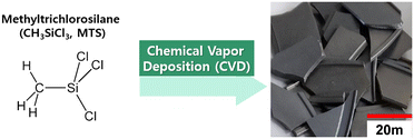
Fig. 1 shows the CVD-SiC source used for the PVT growth of SiC crystals in this study. As described in the introduction, the CVD-SiC components are synthesized from MTS via the CVD process and shaped for semiconductor use via mechanical processes. N is doped in the CVD process to have electric conductivity for the semiconductor process applications. After semiconductor process usages, the CVD-SiC components are crushed to be prepared as the source for crystal growth, as shown in Fig. 1. The CVD-SiC source was prepared as a thin plate with an average thickness of ∼0.5 mm and a mean particle size of 49.75 mm.
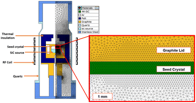
From the CVD-SiC sources shown in Fig. 1, SiC crystals were grown in the induction heating furnace via the PVT method. To evaluate the temperature distribution of the hot zone, a commercial simulation code, VR-PVT 8.2 (STR, Republic of Serbia) was used.10 The reactor with the hot zone was modelled as a 2D axis-symmetric model, as shown in Fig. 2 with its meshed model. All the materials used in the simulation are shown in Fig. 2, and their properties are listed in Table 1.8–11 Based on the simulation, 2 inch SiC crystals were grown via the PVT method at the temperature range of 2250–2350 °C for 4 hours under 35 Torr in an Ar atmosphere. A 4° off-axis 4H-SiC wafer was used for the SiC seed. The grown crystals were evaluated using micro-Raman spectroscopy (Witec, UHTS 300, Germany) and high-resolution XRD (HRXRD, X'Pert-PROMED, PANalytical, the Netherlands). The concentrations of impurities in the grown SiC crystals were evaluated using dynamic secondary ion mass spectrometry (SIMS, Cameca IMS-6f, France). The dislocation densities of the grown crystals were evaluated with synchrotron white beam X-ray topography at the Pohang Light Source.
 | ||
| Fig. 2 Drawings of the hot-zone for PVT growth in the induction heating furnace and its meshed model. | ||
| Properties [unit] | SiC (crystal)10,11 | SiC (source)8–10 | Graphite10 | Felt10 | Quartz10 | Ar (ref. 10) | Stainless steel10 |
|---|---|---|---|---|---|---|---|
| Density [kg m−3] | 3220 (ref. 11) | 3210 (ref. 9) | 1950 | 120 | 2210 | — | 7850 |
| Thermal conductivity [W m−1 K−1] | 288 (ref. 10) | 203.7 (ref. 8) | 150 | 0.336 | 1.4 | 1 | 44.5 |
| Heat capacity [J kg−1 K−1] | 1000 (ref. 10) | 1000 (ref. 10) | 710 | 200 | 730 | — | 475 |
| Surface emissivity | 0.9 (ref. 11) | 0.6 (ref. 10) | 0.9 | 0.8 | 0.01 | — | 0.1 |
| Electrical conductivity [S m−1] | 1000 (ref. 10) | 1000 (ref. 10) | 75![[thin space (1/6-em)]](https://www.rsc.org/images/entities/char_2009.gif) 400 400 |
430 | 1 × 10⁻¹⁴ | 1 | 1.7 × 10⁶ |
Since both the HTCVD method and PVT method grow crystals in the equilibrium state of the gas–solid phase at the growth front, the successful rapid growth of SiC via the HTCVD method leads to the challenge of the rapid growth of SiC via the PVT method in this study. While the HTCVD method uses a gaseous source with easy flow control, the PVT method uses a solid source that is not directly flow controlled. Of course, the flow rate supplied to the growth front in the PVT method could be controlled by the sublimation amount of the solid source by controlling the temperature distribution, but the precise control of temperature distribution in the PVT method is not easily achieved in real growing systems.
By increasing the temperature of the source in the PVT reactor, the growth rate of SiC could be increased by increasing the flow rate of the sublimed sources. To realize stable crystal growth, temperature control at the growth front is especially important.2–5 To increase the growth rate without polycrystal formation, a high-temperature gradient at the growth front is required as demonstrated in SiC growth via the HTCVD method.2–5 The thermal conduction along the vertical direction to the backside of the lid is not sufficiently big, and the accumulated heat at the growth front should be dissipated to the growth surface by thermal radiation, resulting in the formation of excess surfaces which means the polycrystal growth.3
Both the mass transfer and the recrystallization process of the PVT method are quite similar to those of the HTCVD method, despite their difference in the SiC sources. This means that the rapid growth of SiC is also achievable when the sublimation rate of the SiC source is sufficiently high. However, there have been several reasons why high-quality SiC single crystals via the PVT method could not be achieved under high growth conditions so far. In general, commercial powders contain a mixture of small and large particles, and due to the difference in surface energy, small particles have relatively high impurity concentration and are sublimated before large particles, which causes high impurity concentration in the grown crystals at the beginning of growth. In addition, since solid SiC is decomposed into solid C and vapor species such as Si, SiC2, and Si2C at high temperatures, solid C is inevitably formed when the SiC source is sublimed in the PVT method. If the formed solid C is sufficiently small and light, the small C particles, the so-called “C dust”, could be transported to the crystal surface with strong mass transport under rapid growth conditions and result in inclusions in the growth crystal. To reduce the metal impurities and the C dust, therefore, the particle size of the SiC sources was typically required to be no more than 200 μm in diameter, while the growth rate was controlled to be not higher than ∼0.4 mm h−1 to maintain slow mass transport excluding the flying C dust. The metal impurities and the C dust cause the degradation of grown SiC crystals, which have been the main barrier preventing the rapid growth of SiC via the PVT method.
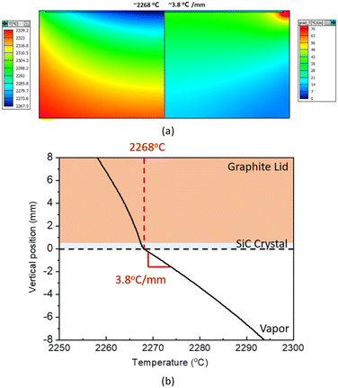
In this study, the flying C dust under strong mass transport is excluded by adopting the crushed CVD-SiC sources which do not contain small particles. Hence, we designed the hot-zone structures to achieve rapid growth of SiC via the PVT method based on multiphysics simulations, and the temperature distribution and the temperature gradient from the simulations are shown in Fig. 3a.
 | ||
| Fig. 3 (a) Temperature distribution and temperature gradient in the PVT reactor near the growth front obtained with FE analysis and (b) vertical temperature distribution along axisymmetric line. | ||
Compared to a typical hot-zone setup for growing SiC crystals at a growth rate of 0.3 to 0.8 mm h−1 under a small temperature gradient below 1 °C mm−1, the hot-zone setup in this study had a relatively large temperature gradient of ∼3.8 °C mm−1 at a growth temperature of ∼2268 °C. The temperature gradient value in this study is comparable to the case of the rapid growth of SiC via the HTCVD method at the growth rate of 2.4 mm h−1, where the temperature gradients were set to ∼14 °C mm−1.3 From the vertical temperature distribution shown in Fig. 3b, we confirmed no inverse temperature gradient near the growth front that could form polycrystals, as explained in the literature.3
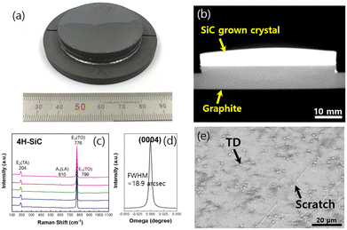
The SiC crystals were grown for 4 hours from the CVD-SiC source in the PVT system, as explained in Fig. 2 and 3. From the number of SiC growths, a representative growth of the SiC crystal was selected and is shown in Fig. 4a. The thickness and the growth rate of the grown SiC crystal shown in Fig. 4a were 5.84 mm and 1.46 mm h−1, respectively. The effect of the SiC source on crystal quality, polytype, morphology, and purity of the grown SiC crystals shown in Fig. 4a was investigated, as shown in Fig. 4b–e. The cross-sectional tomographic image in Fig. 4b showed that the crystal was grown as a convex shape since their growing conditions were not fully optimized. According to the micro-Raman spectra shown in Fig. 4c, however, the grown crystals were identified as a single phase of 4H-SiC without any polytype inclusion. The full-width at half maximum (FWHM) value obtained with X-ray rocking curve analysis was 18.9 arcsec for the (0004) peak, which also confirms good crystal quality.
Fig. 4e shows white beam X-ray topography identifying scratches and threading dislocations in the polished wafer for the grown crystal. The dislocation density of the grown crystal was measured as ∼3000 ea cm−2, which was slightly more than the dislocation density of the seed crystal, ∼2000 ea cm−2. The grown crystal was confirmed to have a relatively small dislocation density, which is comparable to the crystal quality of commercial wafers. It was interesting to note that the rapid growth of the SiC crystal was achieved with the PVT method under a big temperature gradient by adopting the CVD-SiC crushed block as the source. The concentrations of B, Al, and N in the grown crystal were measured as 2.18 × 10¹⁶, 7.61 × 10¹⁵, and 1.98 × 10¹⁹ atom per cm3, respectively. The concentration of P in the grown crystal was below the detection limit of P (<1.0 × 10¹⁴ atom per cm3). The concentrations of the impurities acting as charge carriers were sufficiently low except N, which was intentionally doped in the CVD process.
Though the crystal growth in this study was small-scaled considering the commercialized products, it was meaningful that the rapid growth of SiC with good crystal quality via the PVT method was successfully demonstrated by adopting the CVD-SiC source. Since the CVD-SiC source has cost competitiveness by recycling discarded materials despite its excellent performance, we expect its popular utilization as a promising SiC source to replace the powder-form SiC sources. To apply the CVD-SiC source to the rapid growth of SiC, the temperature distribution of the PVT system needs to be optimized, which opens further issues to be studied from now on.
Conclusions
In this study, the rapid growth of SiC crystals via the PVT method is successfully demonstrated under high-temperature gradient conditions by adopting the crushed CVD-SiC blocks. It was interesting to note that the rapid growth of SiC crystals was achieved with the PVT method by replacing the SiC source. This method is expected to significantly improve the mass-producibility of SiC single-crystal fabrication, ultimately reducing the unit cost of SiC substrates and improving the spread of high-performance power devices.Author contributions
Seong-Min Jeong was responsible for the conceptualization of the research and the drafting of the manuscript. Yong-Hyeon Kim and Ju-Hyeong Sun jointly conducted the experimental growth of crystals and performed detailed inspections of the resulting crystals. Jae-Hyeon Park executed the simulations related to the crystal growth process. Data analysis was carried out by Yun-Ji Shin and Si-Young Bae, focusing on interpreting the experimental results. The provision of material sources and access to experimental facilities were managed by Chang-Min Kim and Won-Jae Lee.Conflicts of interest
There are no conflicts to declare.Acknowledgements
This work was financially supported by the KICET strategic research program (No. KPP23004) funded by the Korea Institute of Ceramic Engineering and Technology.References
- T. Kimoto and J. A. Cooper, Fundamentals of silicon carbide technology: growth, characterization, devices, and applications, John Wiley & Sons Singapore Pte. Ltd., Singapore, 2014 Search PubMed.
- N. Hoshino, I. Kamata, T. Kanda, Y. Tokuda, H. Kuno and H. Tsuchida, Appl. Phys. Express, 2000, 13, 095502 CrossRef.
- Y. Tokuda, E. Makino, N. Sugiyama, I. Kamata, N. Hoshino, J. Kojima, K. Hara and H. Tsuchida, J. Cryst. Growth, 2016, 448, 29 CrossRef CAS.
- N. Hoshino, I. Kamata, Y. Tokuda, E. Makino, T. Kanda, N. Sugiyama, H. Kuno, J. Kojima and H. Tsuchida, J. Cryst. Growth, 2017, 478, 9 CrossRef CAS.
- Y. Tokuda, N. Hoshino, H. Kuno, H. Uehigashi, T. Okamoto, T. Kanda, N. Ohya, I. Kamata and H. Tsuchida, Mater. Sci. Forum, 2020, 1004, 5 Search PubMed.
- F. Loumagne, F. Langlais and R. Naslain, J. Cryst. Growth, 1995, 155, 198 CrossRef CAS.
- G. Chichignoud, M. Ucar-Morais, M. Pons and E. Blanquet, Surf. Coat. Technol., 2007, 201, 8888 CrossRef CAS.
- Tokai Carbon Korea Co. Ltd., https://www.tck.co.kr/eng/business/SolidSiC.php, (accessed 23 February 2024).
- Hana Materials Inc., https://en.hanamts.com/product-temp2/, (accessed 23 February 2024).
- STR Group, https://str-soft.com/crystal-growth/pvt-sic/, (accessed 23 February 2024).
- H. Luo, X. Han, Y. Huang, D. Yang and X. Pi, Crystals, 2021, 11, 1581 CrossRef CAS.
| This journal is © The Royal Society of Chemistry 2024 |


