 Open Access Article
Stacking engineering in layered homostructures: transitioning from 2D to 3D architectures
Jiamin
Wang
ab,
Fang
Cheng
c,
Yan
Sun
 *d,
Hai
Xu
*abe and
Liang
Cao
 *f
*f
aChangchun Institute of Optics, Fine Mechanics & Physics (CIOMP), Chinese Academy of Sciences, Changchun 130033, P. R. China. E-mail: xuhai@ciomp.ac.cn
bUniversity of Chinese Academy of Sciences, Chinese Academy of Sciences, Beijing 100049, P. R. China
cState Key Laboratory for Organic Electronics and Information Displays & Jiangsu Key Laboratory for Biosensors, Institute of Advanced Materials (IAM), Jiangsu National Synergetic Innovation Center for Advanced Materials (SICAM), Nanjing University of Posts and Telecommunications, Nanjing 210023, P. R. China
dInstitutes of Physical Science and Information Technology, Anhui University, Hefei 230601, P. R. China. E-mail: yansun@ahu.edu.cn
eCenter of Materials Science and Optoelectronics Engineering, University of Chinese Academy of Sciences, Beijing 100049, P. R. China
fAnhui Key Laboratory of Low-Energy Quantum Materials and Devices, High Magnetic Field Laboratory, HFIPS, Chinese Academy of Sciences, Hefei 230031, P. R. China. E-mail: lcao@hmfl.ac.cn
First published on 12th February 2024
Abstract
Artificial materials, characterized by their distinctive properties and customized functionalities, occupy a central role in a wide range of applications including electronics, spintronics, optoelectronics, catalysis, and energy storage. The emergence of atomically thin two-dimensional (2D) materials has driven the creation of artificial heterostructures, harnessing the potential of combining various 2D building blocks with complementary properties through the art of stacking engineering. The promising outcomes achieved for heterostructures have spurred an inquisitive exploration of homostructures, where identical 2D layers are precisely stacked. This perspective primarily focuses on the field of stacking engineering within layered homostructures, where precise control over translational or rotational degrees of freedom between vertically stacked planes or layers is paramount. In particular, we provide an overview of recent advancements in the stacking engineering applied to 2D homostructures. Additionally, we will shed light on research endeavors venturing into three-dimensional (3D) structures, which allow us to proactively address the limitations associated with artificial 2D homostructures. We anticipate that the breakthroughs in stacking engineering in 3D materials will provide valuable insights into the mechanisms governing stacking effects. Such advancements have the potential to unlock the full capability of artificial layered homostructures, propelling the future development of materials, physics, and device applications.
1. Introduction
In 2004, graphene was successfully mechanically exfoliated from its three-dimensional (3D) counterpart of highly oriented pyrolytic graphite (HOPG).1 The exceptional characteristics confined within this two-dimensional (2D) limit of monolayer structure, including the quantum Hall effect,2,3 excellent thermal conductivity,4 high mechanical strength,5 and ultra-high carrier mobility,3 make graphene a promising material for a wide range of applications. Concurrently, substantial research efforts have been devoted to exploiting alternative 2D materials similar to graphene.6–17 Numerous materials such as transition metal dichalcogenides (TMDs),6,12 hexagonal boron nitride/carbonitride (h-BN/h-BCN),7–9 transition metal carbides/nitrides (MXenes),13,14 silicene,15 phosphorene,9,10 and borophene16,17 have been reported to exhibit extraordinary (opto)electrical, optical, magnetic, mechanical, thermal and emergent properties.In addition to the pursuit of new artificial layered materials, the realm of stacking engineering in 2D materials presents promising prospects. Notably, the absence of dangling bonds on the surface of layered materials and the favorable van der Waals (vdW) interactions between layers facilitate the restacking of layered materials into artificial heterostructures.18–20 This stacking engineering approach not only overcomes lattice mismatch challenges but also permits the amalgamation of diverse 2D material building blocks, each endowed with complementary properties, resulting in the creation of tailored functionalities.19–21
While significant progress has been made in constructing heterostructures featuring distinct 2D building layers,12,19,20 there is a concurrent shift in focus towards the exploration of 2D homostructures, characterized by identical 2D layers.22Fig. 1 illustrates the chronological roadmap of breakthroughs in stacking engineering in layered homostructures and outlines the future trends from 2D to 3D. The emergent properties of stacked bi-/tri-layered homostructures achieved by controlling twist angles and lateral sliding between adjacent layers in 2018 and 2021, respectively, have given rise to the emerging fields of twistronics23,24 and slidetronics.25,26 These fields are fundamentally driven by the modulation of structural symmetry. In addition, heterophase homostructures formed by distinct structural phases of chemically homogeneous materials can be achieved by intra-layer atomic sliding proposed in monolayer TMDs in 2014. These structures exhibit exotic properties due to alteration of interlayer coupling. The introduction of new physics and/or mechanisms of 2D homostructures, such as moiré flat bands and sliding ferroelectricity, has led to growing interest in re-evaluating the physical properties of 3D bulk materials hosting a non-centrosymmetric structure. 3R-MoS2, which was obtained 70 years ago,27 is found to exhibit spontaneous polarization in thin film due to the lack of inversion and mirror symmetry associated with natural interlayer sliding.28 Moreover, efforts have been dedicated to the controlled vertical stacking of 2D layers in 3D bulk structures, with the introduction of symmetry-breaking elements. The aim is to address the challenges faced by 2D homostructures, such as environmental instability, poor scalability, and limited defect tolerance, which hinder the commercial applications of 2D materials.
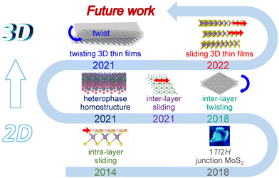 | ||
| Fig. 1 The chronological roadmap of experimental key developments in stacking engineering within layered homostructures, progressing from the 2D to 3D structure. | ||
This perspective aims to provide a comprehensive overview of recent advancements in stacking engineering within layered homostructures, spanning from 2D to 3D structures. As depicted in Fig. 1, the primary focus is on achieving precise control over translational and rotational degrees of freedom between vertically stacked planes or layers. In Section 2, we delve into the morphologies and structural phase transitions in monolayer TMDs induced by changes in intra-layer stacking sequences, as illustrated in the bottom part of Fig. 1. Illusatrated in the middle part of Fig. 1, section 3 outlines the unique features of stacked 2D homostructures, achieved through control of the inter-layer rotational and translational degrees of freedom, as well as the features of heterophase homostructures brought about by specific structural phase transitions, highlighting key recent studies. The endeavors made in stacking engineering within 3D structures are described in Section 4, as illustrated in the top part of Fig. 1. Additionally, we provide an outlook on the future opportunities that lie within stacking engineering in layered 3D bulk materials.
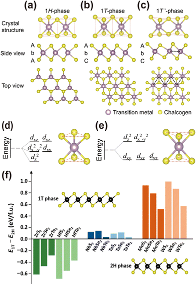 | ||
| Fig. 2 Atomic layer structures of (a) the 1H-phase, (b) 1T-phase and (c) 1T′-phase of monolayer TMDs. Schematic of energy splitting of transition metal d-orbitals in (d) trigonal prismatic H and (e) octahedral T crystal structures. (f) The energy difference between 1T- and 1H-phases for groups 4, 5, and 6 TMDs calculated by using DFT.30 Reprinted with permission from ref. 30. Copyright 2018, American Chemical Society. | ||
2. Single layer TMD materials
2.1 Structural phase of monolayer TMDs
TMD materials are composed of transition metal atoms (M), typically from group-4 to group-10 of the periodic table, bonded to chalcogen atoms (X), such as sulfur, selenium, or tellurium, denoted as MX2.6,29 Unlike traditional 3D materials, TMD crystals exhibit a quasi-2D layered structure, characterized by stacked MX2 layers held together by vdW forces, making monolayer TMDs stable 2D materials. However, differing from graphene with a truly monolayer atomic structure, monolayer TMDs feature a triple-atomic-layer structure, where a transition metal layer is sandwiched between two chalcogen atomic layers.29In the monolayer structure of MX2, the on top stacking of two chalcogen atomic layers leads to the trigonal prismatic coordination of metal atoms. The formed 1H-phase exhibits out-of-plane chalcogen–metal–chalcogen elemental AbA arrangements, as illustrated in Fig. 2(a). By rotating the top chalcogen layer by 60° with respective to the bottom chalcogen layer, the octahedral coordination of metal atoms is achieved, forming the 1T-phase. This 1T-phase features out-of-plane elemental AbC arrangements, as shown in Fig. 2(b).12 For some TMDs, the 1T-phase is unstable and will relax to the distorted 1T′-phase due to the formation of metal–metal bonds, as depicted in Fig. 2(c).
The stability of different structural phases (H-, T-, and distorted T′) in monolayer TMDs depends on the ligand field splitting of d-orbitals and the number of d-electrons of transition metals.31,32 The splitting of d-orbitals under trigonal prismatic H and octahedral T crystal fields is illustrated in Fig. 2(d) and (e), respectively. The H-phase presents three energy levels (dz2, dx2–y2,xy and dxz,yz), while the T-phase features two energy levels (dxy,xz,yz and dz2,x2−y2). The coordination preference is determined by the number of electrons occupying the lower energy dz2 orbital. Density functional theory (DFT) calculations generally indicate that group-4 TMDs favor the T-phase, whereas group-5 and group-6 TMDs favor the H-phase (Fig. 2(f)).30 However, exceptions exist, such as WTe2, where the T′-phase with lower periodicity is obtained.33
2.2 Structural phase transition and advancements
The electronic properties of monolayer TMDs in their T- and H-phases are distinctive and are governed by the interaction between the metal d- and chalcogen p-orbitals.34–36 Generally, monolayer T-/T′-MX2 normally exhibits metallic behavior due to the partial filling of the lowest dxy,xz,yz orbitals. This metallic character holds promise for applications in electrocatalysis and energy storage. In contrast, H-MX2 is semiconducting due to the full occupation of the lowest dz2 orbital, resulting in an optical bandgap of 1.0–2.5 eV.37 Notably, monolayers 1H-MoS2 and 1H-WSe2 demonstrate good semiconducting behavior, making them suitable for opto-electronic device applications.38 Furthermore, beyond metallic39,40 and semiconducting electronic phases,34 monolayer TMDs also exhibit a diverse range of electronic phases, including Mott insulating,41 charge density waves (CDWs),42,43 and superconducting states,44 which are subjected to the structural phase. For instance, monolayer 1T-TaS2 is accepted as a Mott-insulator,45–47 whereas monolayer 1H-TaS2 is a superconductor.48,49 Additionally, specific TMDs manifest topological electronic phases, such as the quantum spin hall effect in group-6 1T′-MX2.50–54 These electronic phases in T-, T′- and H-phases, whether stable or metastable, are summarized in Fig. 3(a).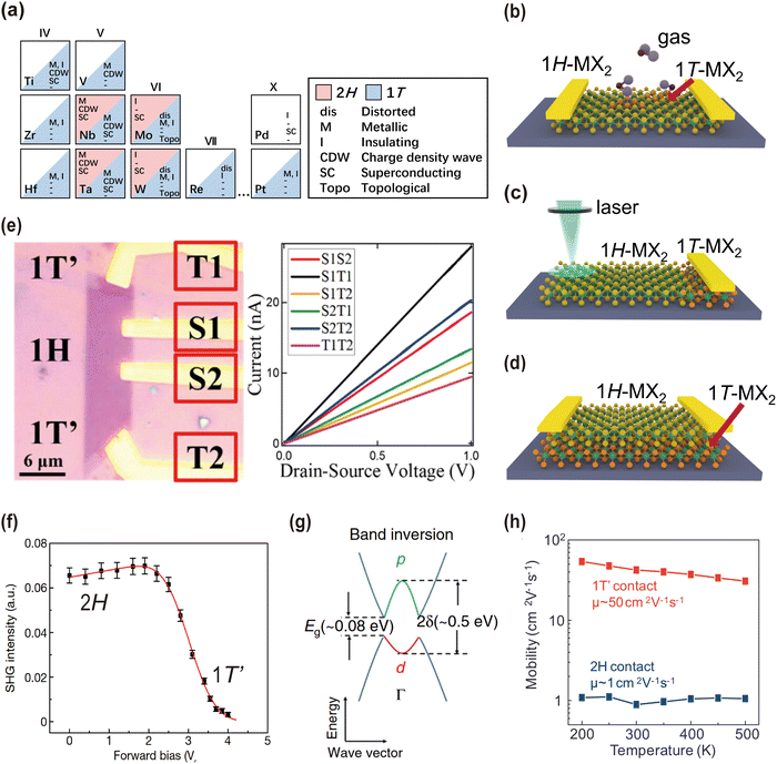 | ||
| Fig. 3 (a) The currently known existing structural phases (2H, 1T or distorted T) and the observed electronic phases of the layered TMDs.12 Reprinted with permission from ref. 12. Copyright 2017, Macmillan Publishers Limited. The schematic of (b) sensing and actuating devices utilizing MX2, (c) lateral 1T/1H MX2 heterophase homostructures and (d) vertical 1T/1H MX2 heterophase homostructures. (e) The optical micrograph of the 1T′–1H–1T′ MoTe2 field effect transistor device and the current–bias voltage (I–V) characteristics of all possible connections.55 Reprinted with permission from ref. 55. Copyright 2017, American Chemical Society. (f) The variation of SHG intensity of monolayer MoTe2 under forward bias. An increase in voltage bias results in the formation of the T′-phase, exhibiting a pronounced decrease in SHG intensity.56 Reprinted with permission from ref. 56. Copyright 2017, Springer Nature. (g) The band structure of 1T′-MoS2 shows a fundamental gap (Eg) and an inverted gap (2δ).50 Reprinted with permission from ref. 50. Copyright 2017, Springer Nature. (h) Variation of the carrier field-effect mobility with temperature for 2H-MoTe2 and 1T′-MoTe2 contacts.57 Reprinted with permission from ref. 57. Copyright 2015, The American Association for the Advancement of Science. | ||
The sandwiched stacking arrangement of monolayer TMDs with X–M–X′ triple-atomic-layers introduces additional translational or rotational degrees of freedom, offering opportunities for stacking engineering, often termed a structural phase transition. Due to their distinct electronic properties, such as metallic T-phases and semiconducting H-phases, phase transition can alter the properties of monolayer TMDs, without the need for the introduction of additional atoms.58 It is widely accepted that electron injection can trigger the structural phase transition. Thus, various external stimuli, including laser irradiation,57 electron beam irradiation,59 electric field,60 magnetic field,61 thermal heating,62 electrostatic doping,56,63 mechanical strain,64–67 absorption,68,69 pressure,70–72 chemical intercalation,73–78 and proton intercalation,79 have been identified as effective strategies. For a more detailed description and summary, readers are recommended to refer to excellent reviews written by Yao Xiao80 and by Xinmao Yin.81
Here, we provide brief examples based on the advancements in structural phase transition of TMDs.
(i) Reversible phase transitions and sensing devices: the reversible transition between the H-phase and T-/T′-phase can be achieved through distinct external stimuli. For instance, alkali metal intercalation, such as Li-ions, can donate electrons to group-6 1H-MX2, inducing a transition from the semiconducting 1H-phase to metallic 1T-phase, whereas a mild annealing process can gradually restore the 1H-phase.73 Other stimuli, such as electrostatic doping,82,83 mechanical strain,64–67 pressure,70–72 and absorption of gases, chemicals and biomolecules (Fig. 3(b)),68,69,78,84 can also initiate phase transitions. The changes in electronic conductivity (Fig. 3(e)), and optical response of different structural phases, such as second-harmonic generation (SHG) characterization of lattice symmetry (Fig. 3(f)) and Raman characterization,83,85 are highly sensitive and selective. These characteristics make them suitable for applications in sensing and actuating devices.
(ii) Irreversible transition to the metastable phase: currently, one of the primary methods for producing monolayer TMDs involves exfoliation from bulk TMD materials. However, the experimental synthesis of metastable bulk TMDs remains a challenge, hindering the direct preparation of the corresponding metastable monolayers. In this regard, inducing irreversible phase transitions from stable phases represents a promising strategy to access metastable phases and elucidate their physical properties. For example, the charge transfer along with interfacial tensile strain occurring at 1H-MoS2/metal interfaces triggers a transition to 1T′-MoS2,86,87 which is proposed to be a quantum spin hall insulator (Fig. 3(g)).50
(iii) Creation of lateral heterophase homostructures: the irreversible and area-selective transition from the stable H-phase (T-phase) to metastable T-/T′-phase (H-phase) can be triggered by high-energy particle irradiation, such as electron beam,59 ion beam88 and laser irradiation.89 These methods offer advantages, such as local patterning, controllable intensity, and high efficiency. The area-selective phase transition results in the creation of lateral 1T/1H heterophase homostructures (cf.Fig. 3(c)). The reduced contact resistance improves the performance of transistor devices by yielding low subthreshold swing values and large on/off ratios.75 As an illustration, laser irradiation of 1H-MoTe2 generates Te-vacancies, causing a transition from the semiconducting H-phase to metallic T′-phase with controlled patterning.57 The covalent bonds at the phase boundary and matched work function between H- and T-phases facilitate the formation of an ohmic heterophase homostructure. The reduced electron scattering at the electrode/1T-MoTe2/1H-MoTe2 interfaces results in an increased carrier mobility, which is 50 times higher than that at the electrode/1H-MoTe2 interface (Fig. 3(h)). Consequently, a high and thermally stable on/off current ratio of 106 is achieved.
(iv) Fabrication of vertical heterophase homostructures: monolayer phase transition enables the fabrication of vertical heterophase homostructures, or 1H-/1T-MX2, as illustrated in Fig. 3(d) by minimizing the risk of contamination during the transfer or film deposition process. This allows for the construction of distinct electronic phases associated with H- and T-phases. This feature, combined with the rich variety of chemical compositions, positions TMDs as an excellent platform for exploring emergent properties, such as Majorana fermions90 and Kondo lattice,91 due to the complex interaction between combined electronic states.92–100 Further details will be discussed in Section 3.3.
In other words, the above is just a few examples of the applications that can benefit from the structural phase transitions in monolayer TMDs. The ability to control and manipulate these transitions opens up new avenues for tailoring the properties of TMDs and exploring their potential in various technological domains. Although significant progress has been made, the precise control of structural phase transition remains a challenge, particularly concerning achieving a complete transition to the target phases.
2.3 Mechanism of structural phase transition
The kinetics and transformation pathways of structural phase transitions in monolayer TMDs are still open questions. Within this unique “monolayer homostructure” of TMDs, the sliding of atomic layers kinetically within the sandwiched structure plays a crucial role.101 This sliding is facilitated by the reduction of elastic energy constraints in 2D materials. Fig. 4(a) illustrates the phase transition from H- to T-phases, as well as from H- to 60° (or 180°) rotational H′-phases in monolayer 1H-MoS2, achieved through intra-layer S- and Mo-plane sliding, respectively.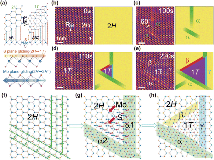 | ||
| Fig. 4 Intra-layer atomic layer sliding induced structural phase transition. (a) Schematic of 1H- to 1T- and 1H- to 1H′-phase transition of monolayer MoS2 in basal plane and cross-sectional views. STEM images along with the corresponding schematic illustrations of (b) monolayer 1H-MoS2 doped with Re substitution dopants and atomic movement 1H- to 1T-phase transition at (c) t = 100 s; (d) t = 110 s; (e) t = 220 s. Schematic of (f) α-phase nucleation, (g) sliding in the S- and Mo-planes leading to the transition tendency from the H-phase to the T-phase, and (h) formation of the T-phase. Three different boundaries are found at three edges between the 1T- and 1H-phases.59 Reprinted with permission from ref. 59. Copyright 2014, Springer Nature Limited. | ||
To monitor the dynamic process of structural phase transition, in situ structural studies in both real space and reciprocal space are highly desirable.80,81Fig. 4(b)–(e) present the as-sequential aberration-corrected scanning transmission electron microscopy (STEM) images of monolayer 1H-MoS2 at 600 °C, along with the corresponding schematic illustrations.59 The heating provides the activation energy for atom displacement, and continuous electron beam irradiation during STEM measurement triggers the atomic displacement in the initially exfoliated Re-doped H-MoS2 monolayer (Fig. 4(b)). After 100 s, constriction of three Mo zigzag chains as illustrated in Fig. 4(f) leads to two non-parallel intermediate α-phase bands, as shown in Fig. 4(c). At 110 s, 1T-MoS2 has emerged at the corner of the contacted α-phase bands (Fig. 4(d)), resulting from the sliding of S- and Mo-atoms as illustrated in Fig. 4(g). This newly formed 1T-phase enlarges in size with further electron beam irradiation (Fig. 4(e)). Simultaneously, two β- and γ-boundaries with structures illustrated in Fig. 4(h) are observed. Notably, the Re-dopants substituting Mo-atoms serve as n-type dopants.102 The additional electrons provided by Re-atoms facilitate the atomic arrangement distortion, which explains the nucleation tendency of the α-phase at the vicinity of Re dopants (Fig. 4(d)).
In addition to the atom mechanism, accompanying changes in electronic structures and vibrational properties can provide valuable insights into the charge mechanism of structural phase transition. Synchrotron-based time-resolved techniques, such as time-resolved and angle-resolved photoemission spectroscopy (tr-ARPES),103 and infrared and Raman spectroscopy,104,105 offer nanometer spatial and femtosecond temporal resolution, making them ideal tools to track the intricacies of intra-layer atomic plane sliding associated with structural phase transitions.
3. Stacking engineering in 2D homostructures
The field of 2D materials expanded to bilayer or multi-layer homostructure systems,106 whose electronic, optical, magnetic, and mechanical properties change dramatically with stacking order.107 In vertically stacked bilayers and multi-layer homostructures, the translational or rotational degrees of freedom are more easily manipulated compared to monolayers. This is due to the weaker out-of-plane vdW interaction and the stronger in-plane covalent bonding, resulting in smaller energy barriers. Recent findings have highlighted that the inter-layer twisting and sliding in these structures offer intriguing electronic properties and fascinating physics not found in the constituent layers,20,108 opening two new fields of “twistronics” and “slidetronics”. Both fields are still at their early development stages and hold infinite possibilities.3.1 Stacked 2D homostructures by inter-layer twisting
In 2018, unconventional superconductivity in bilayer graphene was discovered by rotation of the top graphene layer with respect to the bottom one by the “magic angle” of 1.1°.23 The small twist angle induces the intriguing electronic properties distinguishing from the constituent layer. This breakthrough has catalyzed the technological, experimental, and theoretical progress of restacked 2D materials, leading to the emergence of the field of “twistronics”, which explores the interplay between the twist angles and electronics.Several techniques have been developed to accurately manipulate and control the fabrication of stacked 2D materials with desired twist angles and to identify these angles. The stacking techniques include tear-and-stack,109 optical alignment of crystal edges,110 and in situ rotation mediated by atomic force microscopy tips.111 The tear-and-stack technique is commonly used for fabricating homobilayers and homotrilayers. As illustrated in Fig. 5(a)–(d), a hemispherical handle is utilized to pick up a thin h-BN flake and then partially contact a source 2D monolayer. The different interaction strengths between the h-BN-2D monolayer and handle-2D monolayer result in the tearing of the 2D monolayer after lifting the handle. The hemispherical handle is then laterally translated to pick up the remaining part, achieving aligned stacking. The precise control of the twist angle can be achieved by carefully rotating the hemispherical hand during the pick-up sequence. However, the limitations such as restricted sample area, twist angle inhomogeneity, constraint on the number of stacking layers, and poor reproducibility of this technique hinder its large-scale fabrication, characterization, and industrial applications. Recently, millimeter size twisted bilayer graphene has been grown by the plasma-enhanced chemical vapor deposition (CVD) method,112 making it an alternative strategy for large-area homogeneity twisted homobilayer fabrication.
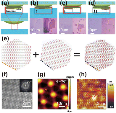 | ||
| Fig. 5 (a)–(d) Illustration of the tear-and-stack technique for a homobilayer with fine twist angle control. (a) Schematic of a hemispherical handle picking h-BN for twisted graphene substrates. The top of panel (b) shows the schematic of the h-BN substrate partially aligned with graphene under an optical microscope. (c) Part of graphene in the monolayer is lifted up by a hemispherical handle substrate with h-BN, rotated at a special angle, and then (d) moved laterally to stack with the remaining graphene on the substrate to achieve precisely aligned twisted bilayer graphene (tBLG). The bottom of panels (b)–(d) illustrated the corresponding optical image.109 Reprinted with permission from ref. 109. Copyright 2016, American Chemical Society. (e) tBLG forming the moiré superlattice.113 Reprinted with permission from ref. 113. Copyright 2017, National Academy of Sciences. (f) High-resolution TEM image of tBLG shows a clear moiré period, and the inset shows the fast Fourier transform (FFT) of the image, which shows precisely the twist angle of 29°.114 Reprinted with permission from ref. 114. Copyright 2016, The Authors, published by Springer Nature. (g) Atomically resolved STM topography of tBLG with a twist angle of 0.79°.115 Reprinted with permission from ref. 115. Copyright 2019, The Authors, under exclusive licence to Springer Nature Limited. (h) Characteristics of tBLG with a twist angle of 5.0° determined using conductive atomic force microscopy (C-AFM), showing a clear atomic stacking structure having a moiré period.116 Reprinted with permission from ref. 116. Copyright 2019, Wiley-VCH Verlag GmbH & Co. KGaA, Weinheim. | ||
Accurately determining the twist angle in stacked 2D layers remains a challenge due to the possibility of relaxation to the energetically favorable configuration. Even slight deviations in the angle can lead to distinct properties. For instance, insulating states and superconductivity were reported in tBLG at a twist angle of ∼0.93°,117 where unconventional superconductivity emerged at ∼1.1°.23 Several effective methods have been developed for predicting and quantifying the twist angle including STEM,114 scanning tunneling microscopy (STM),115 atomic force microscopy (AFM),116 Raman spectroscopy,112 photoluminescence (PL) spectroscopy118 and second-harmonic generation (SHG).119
Fig. 5(e) illustrates the moiré superlattice of bilayer graphene. The STEM, STM, and AFM imaging techniques provide detailed real-space structural characteristics as depicted in Fig. 5(f)–(h), respectively. The twist angles can be determined from the corresponding moiré period. In addition, Raman spectroscopy, PL spectroscopy and SHG serve as powerful tools for determining the twist angle by examining the angular dependence of characteristic signals. The combination of Raman, PL spectroscopy, and SHG allows for a remarkable improvement in the uncertainty to ∼0.01°.
Different inter-lattice interactions at various stacking angles give rise to variations in lattice vibrations. Fig. 6(a) displays the Raman spectra of bilayer graphene, illustrating the evolution of various signature modes with changing twist angles.120 As the twist angle increases, the intensity of the G peak and 2D band attributed to the graphene single layer progressively enhances, exhibiting a distinct angular dependence. At ∼9°, a new feature of R′ appears. At a specific twist angle of ∼12°, R′ disappears and R appears. This is due to the presence of a static potential energy in rotationally stacked bilayer graphene that arises from the interaction between the two layers. This static potential energy can transfer the momentum of light-excited electrons to graphene, leading to a special phenomenon called double-resonance Raman scattering.121 In addition, two additional modes, (ZO′)L and (ZO′)H, accompanied by a strong background, emerge at this twist angle. At a larger twist angle of >20°, all new modes disappear, lifting G and 2D modes.
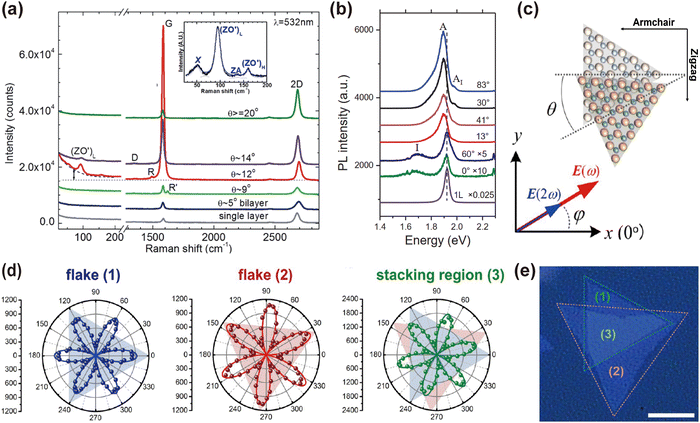 | ||
| Fig. 6 (a) Raman spectra of monolayer and bilayer graphene with different twist angles. The inset shows the energy spectrum after subtracting the background.120 Reprinted with permission from ref. 120. Copyright 2013, American Chemical Society. (b) Comparison of PL spectra of a randomly twisted WS2 bilayer and a 0° and 60° twisted bilayer and monolayer (1L) at a 532 nm excitation wavelength.118 Reprinted with permission from ref. 118. Copyright 2015, Wiley-VCH Verlag GmbH & Co. KGaA, Weinheim. (c) Schematic diagram of bilayer 1H-MoS2 stacked at an angle of θ–25° and (e) the corresponding optical microscopy image. Azimuthal angle φ in panel (c) represents the angle between the incident laser polarization direction and the armchair direction. (d) The polarization-resolved SHG measured in flake (1), flake (2) and stacked areas (3) in (e).122 Reprinted with permission from ref. 122. Copyright 2014, American Chemical Society. | ||
The energy bands are also affected by the inter-layer twist angle, resulting in the change in the PL peaks, making PL an effective method for detecting the twist angle. Fig. 6(b) represents the PL spectra of randomly-twisted WS2 bilayers.118 For on top AA-stacking (0°) and AB-stacking (60°), two major peaks corresponding to the direct transition peak A and the indirect transition peak I are observed. Their intensities show distinct twist angle dependence. The intensity of peak A is enhanced with increased twist angles, whereas peak I disappears.
Twist angle determination can also be achieved through polarization resolved SHG measurement, which detects decoupled signals from top and bottom layers. For the monolayer 1H-MoS2 with three-fold rotational symmetry, I‖ ∝ cos2![[thin space (1/6-em)]](https://www.rsc.org/images/entities/char_2009.gif) 3φ (I⊥ ∝ sin2
3φ (I⊥ ∝ sin2![[thin space (1/6-em)]](https://www.rsc.org/images/entities/char_2009.gif) 3φ), where φ is the azimuthal angle of the incident laser polarization with respect to the armchair direction, as shown in Fig. 6(c). The intensity reaches maximum when the polarization direction of the incident laser is parallel to the armchair direction (φ = 0°). As shown in Fig. 6(d), the polarization-resolved SHG of MoS2 flake (1) and flake (2) (Fig. 6(e)) shows a six-petal pattern with the petals aligned along the vertical bisector of each flake. The SHG of the stacked area (3) also shows a six-petal polarization pattern and the petals are located in the direction between the two nearest vertical bisectors of flake (1) and flake (2). The fitted data for the relative angles of the two sets of petals (φflake1 = 0°, and φflake2 = 25°) yield a twist angle of θ–25° for the stacked MoS2 flakes.122
3φ), where φ is the azimuthal angle of the incident laser polarization with respect to the armchair direction, as shown in Fig. 6(c). The intensity reaches maximum when the polarization direction of the incident laser is parallel to the armchair direction (φ = 0°). As shown in Fig. 6(d), the polarization-resolved SHG of MoS2 flake (1) and flake (2) (Fig. 6(e)) shows a six-petal pattern with the petals aligned along the vertical bisector of each flake. The SHG of the stacked area (3) also shows a six-petal polarization pattern and the petals are located in the direction between the two nearest vertical bisectors of flake (1) and flake (2). The fitted data for the relative angles of the two sets of petals (φflake1 = 0°, and φflake2 = 25°) yield a twist angle of θ–25° for the stacked MoS2 flakes.122
With the ongoing advancement of fabrication and detection techniques, there is a focused effort to conduct in-depth research aiming at uncovering twisted systems and understanding the fundamental aspects of phenomena dependent on twist angles, driving sustained progress in this field.
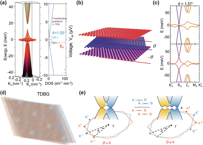 | ||
| Fig. 7 (a) Moiré bands and the corresponding DOS of tBLG with a twist angle of 1.05°. The lowest conduction band and the highest valence band near the Γ point become very flat.23 Reprinted with permission from ref. 23. Copyright 2018, Macmillan Publishers Limited, part of Springer Nature. All rights reserved. (b) Schematic diagram of tTLG. (c) The calculated energy band of tMBLG with (top panel) and without (bottom panel) the electric field.125 Reprinted with permission from ref. 125. Copyright 2021, The Authors, under exclusive licence to Springer Nature Limited. (d) Schematic diagram of tDBG. (e) Two parabolic dispersion bands of tDBG with and without displacement field D.126 Reprinted with permission from ref. 126. Copyright 2020, The Authors, under exclusive licence to Springer Nature Limited. | ||
The moiré flat bands are of wide interest and explored by researchers. The discovery of the flat band in magic angle tBLG has encouraged extensive research in the field.
(i) Emergent phenomena: the formation of a moiré superlattice in tBLG induces the modifications in interlayer coupling. The electron–electron and/or electron–phonon interactions become very strong in this confined geometry, resulting in changes to the band structure. This results in rich electron topology and correlation effects,106,114,116,127–130 as observed in correlated insulating states, spin-polarized correlated states,131 topological edge states,132 topologically protected helical edge states, orbital ferromagnetics,24,133–136 Mott-insulating states, unconventional superconducting states, and Chern insulators.137–142
(ii) Dimensional tunability: increasing the number of graphene layers facilitates effective adjustments of the moiré band through interaction between flat bands and Dirac bands. Fig. 7(b) illustrates the magic angle twisted trilayer graphene (tTLG), featuring aligned top and bottom layers of graphene and a twisted middle layer at a magic angle of ∼1.5°. The calculated electronic band structures with (top panel) and without (bottom panel) the electric field are shown in Fig. 7(c). At the zero electric field, tTLG has a set of flat bands and gapless Dirac bands. By applying an electric field that breaks the mirror symmetry, hybridization between the flat bands and the Dirac bands occurs, which allows controlling the bandwidth and interaction strength in the flat bands.125 Compared to tBLG, tTLG demonstrates a larger moiré superlattice with better electronic structure tunability and superconducting properties.
An additional example is the twisted double bilayer graphene (tDBLG), composed of two AB-stacked BLGs stacked at a certain twist angle (Fig. 7(d)). The corresponding band structure shown in Fig. 7(e) demonstrates more obvious flatness at the top of the valence band and the bottom of the conduction band under the action of an appropriate displacement field D, thus favoring the formation of flat bands.126 These examples demonstrate the multidimensional tunability of graphene stacking systems, which provides an effective platform for the study of strongly correlated systems and opens new avenues for the study of correlated states and topology performance.
(iii) Additional heterostructures: beyond homostructures, considerable efforts have been made to explore similar phenomena in graphene-based moiré systems beyond homostructures, such as twisted graphene/h-BN heterobilayers136 and graphene/MX2 heterobilayers.143 These discoveries provide potential opportunities for understanding and developing novel quantum materials and electronic devices. For detailed information on heterostructures, which is beyond the scope of current discussion, please refer to reviews 144–146.
(i) Unlike graphene, which exhibits sp2 hybridization among carbon-atoms, TMDs involve d orbitals of transition metals, leading to stronger Coulomb interactions. In addition to robust observation of the Mott insulating state, correlated electronic phases, such as the Wigner crystal state, Chern insulating state, strip phase, and antiferromagnetism, are observed in twisted TMD homobilayers.131,147–150
(ii) Unlike single-atomic-layer graphene, monolayer TMDs possess a triple-atomic-layer structure that allows lattice relaxation within the inter-layer space in twisted TMDs. This relaxation leads to the stabilization of flat bands at large twist angles, facilitating the emergence of strong correlation physics across a broad range of twist angles.149 However, this relaxation presents a double-edged sword. The resulting irregularly distributed chalcogen atoms within the inter-layer space complicates the stacking configuration.151 Therefore, careful attention should be given to determining the relationship between the twist angles and properties.
(iii) Depending on their elemental composition and polymorphic structure, TMDs feature a range of physical properties, including metallic behavior, band insulator states, Mott insulator state, CDW states, superconducting states and topological quantum states.80 The continuous tuning of interaction phenomena by adjusting the twist angle enables the exploration of the intricate relationship, including competition, coexistence, or cooperation among intertwined states of Mott-insulating, CDW and superconducting states. Moreover, this twist angle stacking engineering offers an alternative avenue for addressing a fundamental question in the field of high-temperature superconductivity: can unconventional superconductivity emerge in doped Mott insulators?
(iv) Emergent optoelectronic features, such as moiré excitons152 and trions, relying on the strong light–matter interaction and the valley-dependent optical selection rule have been discovered in twisted homobilayers comprised of semiconducting TMDs,153,154 opening up exciting possibilities for their application in valley electronics, nanophotonic devices and quantum technologies.155
Moiré excitons, as illustrated in Fig. 8(a), are quasiparticles formed by combination of an electron and a hole trapped in the moiré superlattice. As neutral particles, they follow bosonic statistics and interact mainly through dipole interactions. The moiré excitons have discrete photoluminescent emission lines with ultra-narrow linewidths (cf.Fig. 8(b)).156 The triple rotational symmetry at the potential energy minimum gives the moiré-trapped exciton a valley character and strong circular polarization properties.
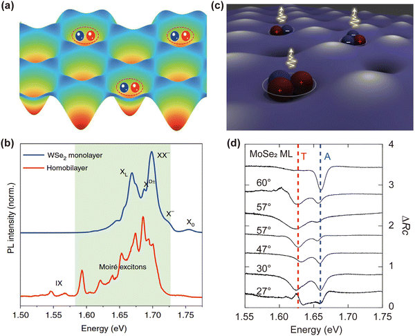 | ||
| Fig. 8 (a) The moiré superlattice leads to the formation of a periodic moiré potential, which traps excitons.160 Reprinted with permission from ref. 160. Copyright 2023, Wiley-VCH GmbH. (b) The PL spectra of monolayer WSe2 and twisted homobilayer WSe2. Many split photoluminescence emission lines emerged in the low energy region for twisted WSe2.156 Reprinted with permission from ref. 156. Copyright 2022, The Authors, under exclusive licence to Springer Nature Limited. (c) Schematic diagram of moiré trions, capturing an exciton with an extra charge carrier.157 Reprinted with permission from ref. 157. Copyright 2021, The Authors, under exclusive licence to Springer Nature Limited. (d) The reflectance contrast (ΔRc) for twisted MoSe2 bilayers. ΔRc = (R − R0)/R0, in which R and R0 represent the sample and background reflectance respectively.161 Reprinted with permission from ref. 161. Copyright 2021, American Chemical Society. | ||
Moiré trions (Fig. 8(c)) are considered to be excitons with an additional charge carrier trapped in the moiré superlattice, resulting in a net charge of +1/−1. Fig. 8(d) shows the reflectance contrast of twisted MoSe2 homobilayers at various twist angles. Besides the free exciton signals guided by a dashed blue line, moiré trion reflectance guided by a dashed red line is enhanced. As charged particles, they follow Fermi statistics, and in addition to dipole interactions, they can interact through long-range Coulomb interactions. The charged nature of moiré trions makes them exhibit unique characteristics in their interaction with external electric and magnetic fields.157 In addition, moiré-trapped trions display distinctive valley properties. Through electron doping, the valley polarization can be switched from a large common circular polarization to a neglected cross-circular polarization; while through hole doping, the valley polarization can be switched from a neglected cross-circular polarization to a large common circular polarization. The found long valley polarization time offers potential for valley electronics applications and emerging nanophotonic devices.158,159
The field of moiré physics in twisted systems is still in its infancy. There are many untapped possibilities for exploring the widely tunable electrical and optical properties, as well as exotic phenomena, arising from the interactions between charge, spin, valley and collective excitations. However, the challenges persist. The limited availability of techniques with high temporal, spatial and energy resolutions, coupled with the absence of experimental probes capable of accessing the various degrees of freedom of charge, spin, lattice, orbital, and valley, hinders an adequate experimental understanding of the underlying physics.
3.2 Stacked 2D homostructures by inter-layer lattice sliding
In addition to rotational degrees of freedom, translational degrees of freedom offer an additional avenue for exploring the exotic properties of stacked 2D homostructures that are not present even in the constituent materials. The phenomenon of sliding ferroelectricity and ability to finely tune the magnetic properties of stacked 2D homostructures, achieved through precise control of inter-layer sliding, have given rise to the emergence of the field of “slidetronics”, which explores the interplay between the inter-layer sliding and electronics.Recently, a significant breakthrough has been achieved with the discovery of sliding ferroelectricity in stacked bilayer h-BN.169 This discovery revealed that the vertical ferroelectric state, which is absent in bulk or monolayer counterparts, can be switched by lateral inter-layer sliding. Fig. 9(a) presents the different stacking configurations of bilayer h-BN. For on top AA′ stacking, which is present in bulk h-BN, wherein the N-(B-) atoms between adjacent layers are vertically aligned, a nonpolar state is expected due to parallel mirror symmetry. However, by lateral sliding the layer by one bond length along the B–N bond direction, an AB arrangement is achieved (cf.Fig. 9(b)). This configuration places the upper N-atoms at the center of the hexagonal lattice of the lower BN layer, while the lower B atom is positioned at the center of the hexagonal lattice of the upper BN layer. The symmetry-breaking causes a net charge transfer, resulting in polarization along the out-of-plane direction. The direction of polarization can be reversed by displacing one h-BN layer by one B–N bond length relative to the other h-BN layer (BA configuration cf.Fig. 9(c)). The weak vdW inter-layer coupling results in ultralow switching barriers compared to vertical ion displacements, enabling high-speed data writing with low energy cost.
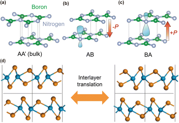 | ||
| Fig. 9 (a–(c) Illustration of the atomic arrangement of AA′, AB, and BA stacking of bilayer h-BN. Nitrogen and boron atoms are shown in silver and green, respectively. AA′ antiparallel stacking with central inversion symmetry and no net charge transfer. AB and BA parallel stacking with perpendicular distortion of the 2pz orbital of nitrogen (light blue), producing an out-of-plane electric dipole.169 Reprinted with permission from ref. 169. Copyright 2021, The Authors, under exclusive licence to Springer Nature Limited. (d) Schematic diagram of inter-layer translation of bilayer TMD with the opposite direction of polarization.170 Reprinted with permission from ref. 170. Copyright 2018, American Chemical Society. | ||
The successful achievement of sliding ferroelectrics, primarily driven by a net charge transfer resulting from inter-layer inequality triggered by lateral sliding, has significantly advanced the burgeoning field of 2D sliding ferroelectricity. In the subsequent two years, numerous homobilayers or homotrilayers, including ReS2 and a series of TMDs such as MoS2, WS2, and MoSe2,171 have been endowed with ferroelectricity via controlled stacking sequences.172 However, not all stacking systems can exhibit ferroelectricity. The fundamental principle underlying sliding ferroelectrics is that (i) vdW bilayers or trilayers are noncentrosymmetric, and (ii) the equivalent state can be achieved through a mirror operation with respect to the horizontal plane in the center and lateral inter-layer translation170 (cf.Fig. 9(d)).
The sliding mechanism underlying the 2D sliding ferroelectrics, distinct from conventional ferroelectricity due to ion displacement, provides advancements from a design viewpoint, described as follows:
(i) Artificial 2D ferroelectrics can be achieved through stacking engineering, utilizing non-ferroelectric monolayers that range from insulators to metals. In conventional ferroelectrics, metallicity and ferroelectricity are considered incompatible because the free-carrier screening effect in metals counteracts the polarization switching induced by an external electric field. However, recent findings have shown that spontaneous polarization can be directly measured in metallic bilayer and trilayer 1T′-WTe2.173,174Fig. 10(a) illustrates the breaking of central inversion symmetry in stacked trilayer structures compared to a 1T′-WTe2 monolayer. Bi-stability, indicating ferroelectric switching characteristics, is observed over a temperature range from 4 K to 250 K (cf.Fig. 10(b)), which is absent in a monolayer (cf.Fig. 10(c)).173
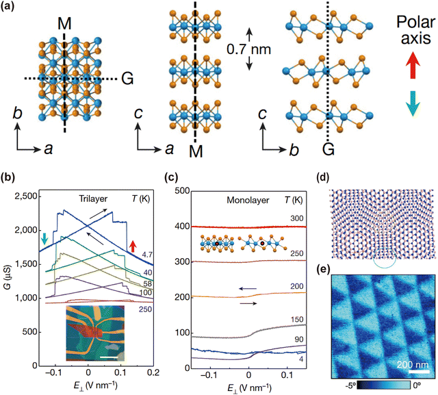 | ||
| Fig. 10 (a) Top view, side view and front view of the 1T′-WTe2 homotrilayer, M represents the mirror plane; G is the sliding plane; red arrow up and green arrow down are polar c-axes. W atoms are in blue; Te atoms are in orange. (b) Conductance G of the undoped trilayer device as E⊥ is swept up and down (black arrows). The plots show bi-stability associated with electric polarization up (red arrow) or down (green arrow), at temperatures from 4 K to 300 K (as labelled). Inset is the optical image of a representative double-gated device. (c) Similar measurements on a monolayer 1T′-WTe2 device (M1), showing no bistability.173 Reprinted with permission from ref. 173. Copyright 2018, Macmillan Publishers Ltd, part of Springer Nature. (d) Schematic diagram of twisted bilayer h-BN forming moiré superlattice ferroelectricity.25 Reprinted with permission from ref. 25. Copyright 2017, American Chemical Society. (e) Twisted h-BN ferroelectric domain image with a triangular period.175 Reprinted with permission from ref. 175. Copyright 2021, The Authors, published by Springer Nature. | ||
These discoveries underscore the significance of lateral lattice sliding as a materials-by-design approach. This approach significantly expands the pool of candidates for designing ferroelectric materials beyond insulators. In addition, the coupling between sliding ferroelectricity and intrinsic physical properties of various 2D building blocks, such as magnetism,176 nontrivial topology,177 excitonics, photonics, electronics, valleytronics, and spin-orbitronics,178 enables the electronic-field control of phenomena for device applications, which warrants further exploration.179 For instance, the slide ferroelectricity in stacked magnetic 2D bilayers facilitates the rational design of 2D multiferroic homostructures hosting ferroelectricity and (anti)ferromagnetism. The magnetoelectric coupling will allow for the electric-field control of magnetism for applications in magnetic memories. The ferroelectric polarization enhances Rashba-type spin orbit coupling, which can be utilized to convert the pure spin current to charge current.180 The switchable polarization will enable the electric-field control of the sign of the charge current for next generation spintronic device applications.
(ii) The 2D materials are stacked at a twist angle in the form of periodic arrangements of AA, AB, and BA, and the polarization directions are also arranged periodically. Fig. 10(d) illustrates the periodic sliding stacking domains formed within twisted bilayer h-BN at a small angle.25 These domains, characterized by AB and BA stacking with opposite polarizations, create a ferroelectric region with periodic changes. Fig. 10(e) shows the periodic triangular ferroelectric domains detected in twisted bilayers h-BN.181 Recently, moiré ferroelectricity has been found in broader homobilayers, including conducting graphene,169 insulating h-BN,175,182 and semiconducting TMDs,183 as well as heterostructures.184–186 These provide promising materials for exploring emergent phenomena due to the interplay between ferroelectricity and twisted correlated electronic states, such as superconductivity, which are not expected to coexist.187
(iii) The atomic-level uniformity of 2D ferroelectrics and their vdW coupling nature, which avoids interface lattice mismatch issues, make them well suited for integration with conventional electronic devices. One of the examples is the integration of ferroelectric materials into field-effect transistors, which can effectively reduce the operation voltage limit and minimize power loss.188
In addition to the dimensionality effect, theoretical calculations predict that the stacking order plays a crucial role in determining the magnetic ground state.206 By altering the stacking order, the transition between antiferromagnetism (AFM) and ferromagnetism (FM) can be achieved. This has been confirmed experimentally in bi-layered CrBr3. Monoclinic R-type (parallel) stacking (Fig. 11(a)) as revealed by STM exhibits antiferromagnetism determined by spin-polarized STS shown in Fig. 11(b), whereas rhombohedral H-type (anti-parallel) stacking (Fig. 11(c)) exhibits ferromagnetism (Fig. 11(d)).207 The inter-layer sliding alters the bond angles and distances of Cr–Br–Br–Cr, and the super exchange interactions controlled by the directional hybridization of the Br p-orbitals and Cr d-orbitals affect the inter-layer coupling and, consequently, the inter-layer magnetism.
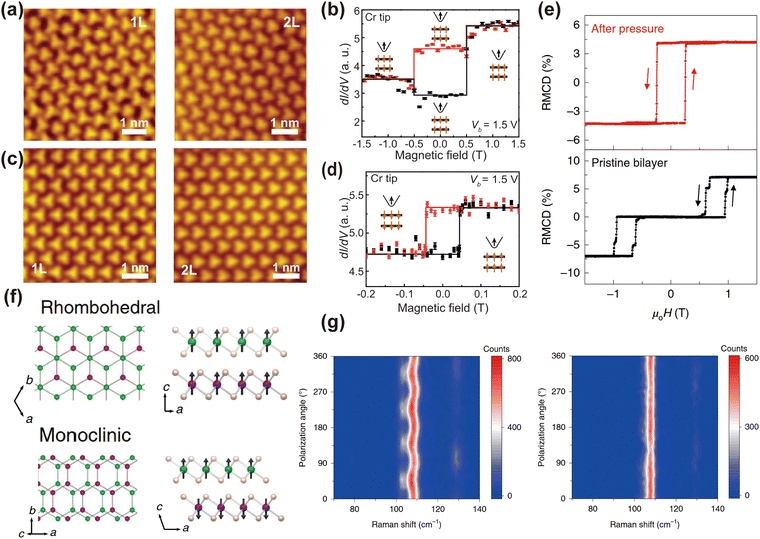 | ||
| Fig. 11 STM images of the bilayer CrBr3 region and its underlying monolayer CrBr3 region, showing (a) the R-type stacking and (c) the H-type stacking. (b) Variation of spin-polarized tunneling with magnetic field in the bilayer region in (a) at Vb = 1.5 V, and (d) in (c) at Vb = 1.5 V. The black line is the upward sweep of the out-of-plane magnetic field and the red line is the downward sweep with a rectangular ferromagnetic hysteresis line.207 Reprinted with permission from ref. 207. Copyright 2019, The American Association for the Advancement of Science. (e) RMCD signals of pristine and stressed bilayer CrI3. (f) Schematic diagram of the bilayer CrI3 stack. The upper diagram indicates a rhombic structure stacking, and the adjacent ferromagnetic monolayers are ferromagnetically coupled. The lower picture indicates the monoclinic structure stacking, and the adjacent ferromagnetic monolayers are antiferromagnetically inter-layer coupled.208 Reprinted with permission from ref. 208. Copyright 2019, The Authors, under exclusive licence to Springer Nature Limited. (g) Polarization angle dependence of Raman spectra of five-layer CrI3 before (left) and after (right) applying pressure at 90 K.209 Reprinted with permission from ref. 209. Copyright 2019, The Authors, under exclusive license to Springer Nature Limited. | ||
The tunability of stacking order in 2D magnetic materials can be triggered by hydrostatic pressure. The reflective magnetic circular dichroism (RMCD) signal shown in Fig. 11(e) indicates that an inter-layer antiferromagnetic to ferromagnetic transition occurs in few layers of CrI3 at sufficiently high pressure.208,209 This phenomenon is attributed to the shift in stacking mode from monoclinic-to-rhombohedral (illustrated in Fig. 11(f)) as evidenced by polarization-related Raman measurements (Fig. 11(g)).
Similar to sliding ferroelectrics, inter-layer twisting (Fig. 12(a)) is another effective approach to fine-tune the magnetic ground states. The coexistence of AFM and FM has been observed in twisted bilayer CrI3,210,211 twisted double-trilayer CrI3, and double-bilayer CrI3212 due to the periodical presence of monoclinic and rhombohedral stacking arrangement, as illustrated in Fig. 12(b)–(d), respectively. However, the question of the influence of moiré superlattice on the magnetic ground states remains open.
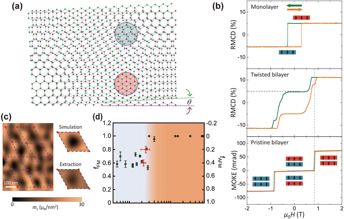 | ||
| Fig. 12 (a) Schematic diagram of twisted bilayer CrI3 showing only Cr atoms, with green (purple) representing the upper (lower) Cr atoms, monoclinic (blue) and rhombohedral (red) periodic arrangement. (b) RMCD and MOKE signals of monolayer, twisted bilayer and pristine bilayer CrI3 as a function of magnetic field. The green and orange curves correspond to decreasing and increasing magnetic fields, respectively. (c) (Left panel) Lattice array of moiré cells. Structure of the moiré cell magnetization extracted from simulations (top right panel) and experimental results (bottom right panel).211 Reprinted with permission from ref. 211. Copyright 2021, The American Association for the Advancement of Science. (d) The ratio of FM and AF varies with the twist angle. At small twist angles, AF and FM coexist; at large twist angles, only FM is present.210 Reprinted with permission from ref. 210. Copyright 2021, The Authors, under exclusive licence to Springer Nature Limited. | ||
Several challenges need to be addressed toward the practical application of stacked 2D magnetic homostructures. Firstly, obtaining large-area few-layer materials remains a significant hurdle. Secondly, the transition temperature of current 2D magnetic homostructures is far below room temperature, limiting their practically. Thirdly, the poor stability in air poses challenges for long-term application. Therefore, substantial efforts are still requested to overcome these challenges in the realm of 2D magnetic materials.
3.3 Heterophase homostructures
Inter-layer twisting and sliding in stacking homostructures with maintained intra-layer structures, as mentioned in the previous subsection, primarily modify inter-layer coupling due to symmetry breaking. Another strategy to alter inter-layer coupling is achieved at the interfaces of heterophases, which are homostructures formed by distinct structural phases of chemically homogeneous materials. As described in Section 2.2, the distinct physical properties exhibited by the T-phase and H-phase of monolayer TMDs make them promising platforms for building 1T-/1H-heterophase homostructures. This, in turn, allows for the improvement of device performance and the exploration of innovative physical behaviors in the fields of electronics, optoelectronics and spintronics.213 For instance, artificial heavy fermions have been observed at the 1T-/1H-TaS2 heterophase homostructure (cf.Fig. 13(a)). These arise from the Kondo coupling between the local magnetic moments confined in the 1T-TaS2 monolayer and conduction electrons of 1H-TaS2.91 As illustrated in Fig. 13(b) and (c), 1T-TaS2 exhibits a flat band structure due to Mott-localization, while 1H-TaS2 displays a metallic band structure, respectively. The electronic hybridization at the 1T-/1H-TaS2 heterophase leads to a heavy-fermion hybridization gap at the 1H-TaS2 side, as illustrated in Fig. 13(d). The creation of 2D Kondo lattices and the associated many-body correlations open up possibilities for exploring unconventional metallic and superconducting states beyond those found in standard correlated materials.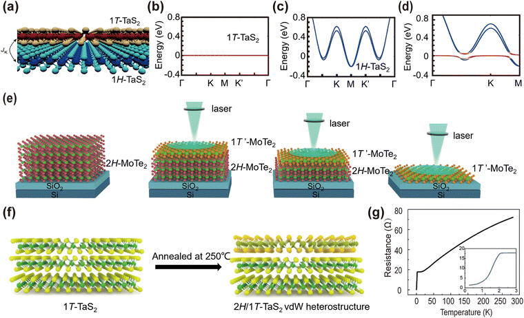 | ||
| Fig. 13 (a) Sketch of the 1T/1H TaS2 heterophase homostructure. (b)–(d) Calculated band structures of 1T, 1H, and 1H/1T bilayer TaS2 heterophase homostructures.91 Reprinted with permission from ref. 91. Copyright 2021, The Authors, under exclusive license to Springer Nature Limited. (e) Schematic diagram of the 1T′/2H MoTe2 homostructure produced by laser radiation.57 Reprinted with permission from ref. 57. Copyright 2015, The American Association for the Advancement of Science. (f) Schematic diagram of the transformation of the bulk TaS2 surface layer into the H-phase by thermal annealing. (g) After annealing, 1T-TaS2 shows a higher superconducting transition temperature at 2.1 K.30 Reprinted with permission from ref. 30. Copyright 2018, American Chemical Society. | ||
Structural phase transitions can be an effective strategy for the fabrication of heterophase homostructure.
As mentioned in Section 2.2, external stimuli can overcome the energy barriers and induce structural phase transitions of as-obtained monolayer TMDs. These external stimuli serve as a promising strategy for the formation of heterophase homostructure with in situ structural modulation. For example, laser irradiation has been utilized to trigger the surface phase transition from 1H-MoTe2 to metallic 1T′-MoTe2 transition, resulting in the creation of an ohmic heterophase homostructure (Fig. 13(e)).57 Thermal annealing can induce the surface 1T-TaS2 to superconducting 1H-TaS2 transition (Fig. 13(f)). The charge transfer resulted in the Fermi level alignment at the 1H-/1T-TaS2 interface, suppressing the CDW state in 1H-TaS2 and enhancing the corresponding superconducting transition temperature (Fig. 13(g)).30 An electric field applied through STM pulse can also trigger a similar surface 1T- to 1H-TaS2 transition,214 although suffering relaxation issue. The magnetic field has been found to cause a 1H- to 1T-MoS2 transition,215 while the properties of the resulting heterophase are less pronounced.
Utilizing external stimuli as a strategy enables in situ structural phase transition and the creation of heterophase homostructures. The resulting clean and sharp interfaces are essential for comprehending the underlying physics mechanisms. However, it is crucial to address the potential unexpected damage introduced by irradiation and thermal treatment, as it can cause the deviations in intrinsic properties. Electric and magnetic fields, serving as non-destructive methods, deserve further investigation despite the challenge related to relaxation.80
Other approaches, including conventional exfoliation and re-stacking techniques and controllable synthesis through direct growth by controlling the synthesis conditions, also contribute to the formation of heterophase homostructures.91,216,217 However, they are beyond the scope of perspective review, which centers on the precise control of translational or rotational degrees of freedom between vertically stacked planes/layers.
In summary, significant process has been made in understanding the interplay of microstructure and physical properties in 2D homostructures, such as twistronics and slidetronics in homobilayers and homotrilayers, as well as exploring emergent physical behaviors in heterophase homostructures. However, several challenges persist.
(i) One major challenge is the lack of large-scale fabrication techniques that can avoid defects and achieve clean interfaces, as these factors significantly affect performance variability in 2D materials based on large-scale circuits.
(ii) The coexistence of twisting and sliding in twisted homostructures complicates the intrinsic physics underlying experimental observations, impeding our understanding of the dominant factors determining physical properties.
(iii) The relaxation from a twisted state or a metastable-polymorph in heterophase homostructures can lead to the degradation of physical properties, thereby limiting their practical applications.
4. Layered 3D materials
The success of stacking engineering in the limited number of homostructures (bi- and tri-layers) raises the question of whether similar phenomena can be achieved in 3D structures, overcoming the issues related to environmental stability, fragility, scalability, and relaxation 2D homostructures suffering. However, the increased dimensionality strongly affects the electrostatic and elastic interactions and therefore physics involved,35,36 presenting a significant challenge for stacking-engineering in layered 3D materials.(i) In 3D bulk materials, the restoration of out-of-plane dielectric screening results in a reduction in the strength of electron–phonon interactions. The ferroelectricity observed in 2D homostructures with restricted dielectric screening in the out-of-plane direction is not expected in a 3D material as the electrical polarization will be fully screened by free electrons. In addition, enhanced dielectric screening hinders the structural phase transformations compared to their 2D counterparts. External stimuli, which are highly effective in controlling structural phase transitions in 2D materials, may not be feasible in 3D materials.
(ii) Owing to the constraint in the out-of-plane direction, the elastic energy penalty along a structural transformation pathway is more significant in 3D materials compared to 2D materials. The substitution of van der Waals adhesion energy with long-range elastic energy fundamentally alters the energy landscape of structural transformation in 3D materials, leading to the slower transformation.
While stacking engineering in 3D bulk materials loses great challenges, driven by the intriguing physics and functionality, attempts have been made to do thin films.
4.1 Inter-layer lattice sliding in layered 3D thin films
The development of translational degrees of freedom in stacked 2D homostructures prompts a re-examination of the ferroelectricity in layered 3D materials, in particular non-centrosymmetric 3R- and 6R-phases of TMDs where inter-layer stacking misalignment occurs naturally.27Fig. 14(a) illustrates the atomic structures of parallel stacked 3R-phase and anti-parallel stacked 2H-phase of TMDs.6,218 In the 2H-phase with AA′ stacking, the presence of inversion symmetry rules out the occurrence of spontaneous polarization along the out-of-plane direction. In contrast, the lack of inversion and mirror symmetry in the 3R-phase facilitates the charge transfer between adjacent atomic layers, leading to the emergence of out-of-plane spontaneous polarization.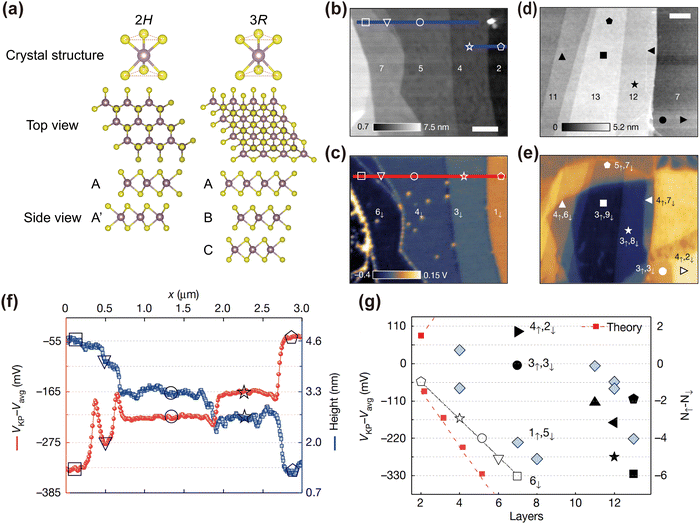 | ||
| Fig. 14 (a) Schematic of the atomic structures of the 2H- and 3R-phases. The (b) image and (c) surface potential map of 3R-MoS2 flakes with 2–7 layers. The (d) image and (e) surface potential map of 3R-MoS2 flakes with 7–13 layers. (f) Flake thickness and surface potential obtained from line cuts marked in panels (b) and (c), respectively. (g) Surface potential values obtained from different positions of various layer numbers, along with the proposed multi-polarization configurations.28 Reprinted with permission from ref. 28. Copyright 2022, The Authors, under exclusive licence to Springer Nature Limited. | ||
Recently, cumulative polarization has been observed at the interfaces between adjacent layers in multilayer regions.28Fig. 14(b) and (c) show the image and surface potential map of naturally grown 3R-MoS2 flakes with 2–7 layers. Fig. 14(f) displays the potential and thickness from the line cut in Fig. 14(b) and (c), respectively. The aligned polarization leads to a linear increase in total polarization as a function of layer number, as guided by the solid black line in Fig. 14(g), demonstrating the cumulative interfacial effect due to the weak coupling between adjacent polarized interfaces.
Fig. 14(d) and (e) present the image and surface potential map of naturally grown 3R-MoS2 flakes with 7–13 layers, respectively. The potential values (cf.Fig. 14(g)) display less dependence on layer number n, suggesting complex interfacial polarization configurations. The multi-polarization states, including upward polarization (N↑) and downward polarization (N↓) and resulting from anti-aligned polarization, are proposed and illustrated in Fig. 14(e). The local potential can be accurately represented by a combination of N↑ and N↓ polarizations. For example, in a specific local stacking configuration with 7 layers, various polarization combinations such as 6↓, 5↓1↑, 4↓2↑, 3↓3↑, 2↓4↑, 1↓5↑, and 6↑ may be detected. Fig. 13(g) shows the detection of four of these combinations. Recently, the cumulative polarization states in the 3R-MoS2 multilayer have been confirmed by the electrical transport measurement.172
Consequently, controlling the stacking sequence of adjacent layers in 3D structures with inter-layer sliding in a similar fashion can enhance the surface potential resulting from co-aligned polarization and promote the emergence of out-of-plane ferroelectricity, which provides further encouragement for future investigations.
4.2 Inter-layer twisting in layered 3D thin films
The first attempt to introduce twisting in an h-BN film (>100 nm) resulted in only one interface with twisting,219 as illustrated in Fig. 15(a). The twist angle was defined as 0° for AA stacking and 60° for AA′ stacking, which occurred naturally, as shown in Fig. 15(b). Positive (negative) twist angles were defined as clockwise (anticlockwise) rotations, as illustrated in Fig. 15(b). The electron diffraction pattern and moiré superlattice of twisted h-BN thin film with twist angles of 2° and 10° are presented in Fig. 15(c)–(f), respectively. To investigate the influence of twist angle on electronic structures, cathodoluminescence (CL) was utilized, involving exciting electrons in materials with high-energy incident electrons. Fig. 15(g) demonstrates that, for the film with the same thickness, the CL intensity at ∼300 nm and room temperature generally increases with an increase in the twist angle from 2° to 27°, and the peak position redshifts. The presence of pinned twisted states without relaxation allows for continuous tuning of twist angles between 30° and −30°. As shown in Fig. 15(h), the CL intensity monotonously increases with twist angles in both positive and negative directions. The band gap determined from the CL emission peak position is found to decrease from 4.5 eV at 0.5° twist angle to 4.0 eV at ±27° twist angle. The calculated moiré flat band at small twist angles reduces the band gap from 5.77 eV to 4.48 eV. The increased bandwidth with twist angles, as calculated from the continuum model, explains the reduction in the energy gap.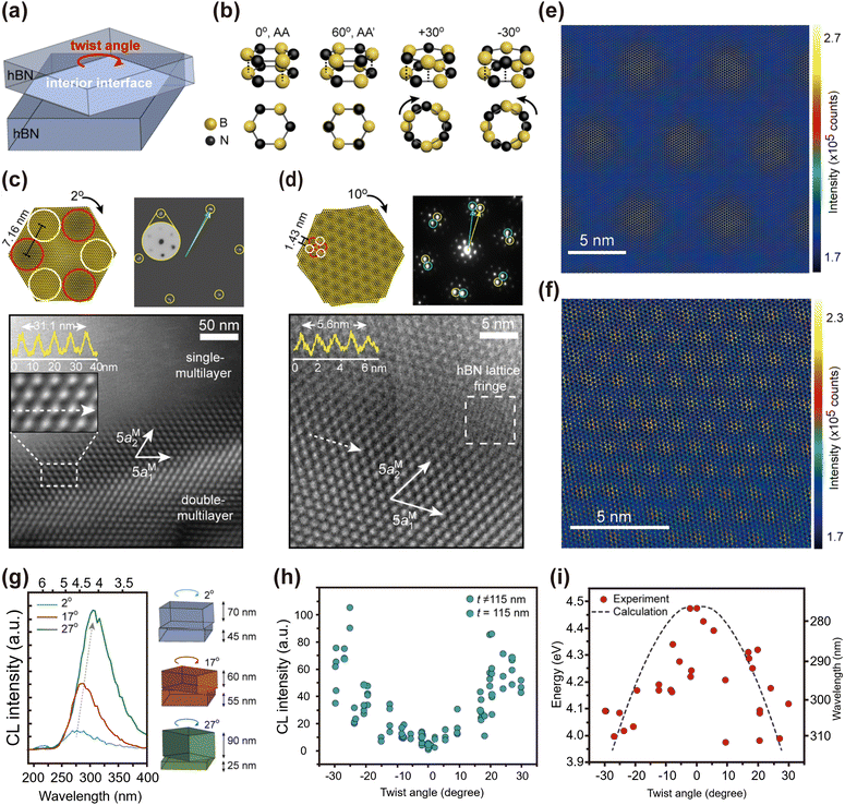 | ||
| Fig. 15 (a) Illustration of a twisted h-BN multilayer with interior interface twisting. (b) Schematics of stacking configuration of two h-BN planar unit cells. (c) Electron diffraction pattern and (d) STEM image of a twisted multilayer with a twist angle of 2°. (e) Electron diffraction pattern and (f) STEM image with a twist angle of 10°. (g) CL spectra of double-multilayer interfaces of the same thickness with different twist angles. The evolution of (h) cathodoluminescence intensity and (i) luminescence energy as a function of twist angles.219 Reprinted with permission from ref. 219. Copyright 2021, American Chemical Society. | ||
The continuous control of the optical emission intensity and energy gap at room temperature enables their practical application. The extension of the twist-related phenomenon from the bi-/tri-layer to thick film makes the manipulation technique easy and overcomes the relaxation issue, paving the way for its industrial compatibility.
5. Outlook
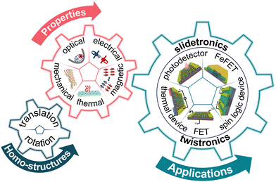
Stacking configurations of vertically stacked layered homostructures have a significant impact on their physical properties due to the modulation of structural symmetry and inter-layer coupling. Fig. 16 illustrates the progression of stacking engineering in layered homostructures. Controlling the rotational and translational degrees of freedom of stacked layered homostructures is thus an effective route to manipulate their properties and explore exotic physics for advanced functionalities. The former results in the burgeoning new field of “twistronics”, wherein the manipulation of the rotation angle of twisted bilayer or multilayer homostructures unveils emergent properties such as unconventional superconductivity, strong electron–electron correlations, orbital ferromagnetism, and topological excitons. Similarly, stacking modulation by lateral inter-layer sliding has also been exploited to alter the electronic, optical and magnetic properties of 2D bilayer or multilayer homostructures, giving rise to a new field termed “slidetronics”. An alternative strategy specific for TMDs is the change of intra-layer stacking sequence, a phenomenon termed structural phase transition. These transitions, most likely achieved by atomic layer translational sliding, lead to the creation of lateral/vertical heterophase homostructures. This not only improves device performance, but also enables the exploration of innovative physical behaviors and functionalities. The advanced functionalities observed in artificial 2D homostructures pave the way for their diverse applications in devices.However, limitations associated with artificial 2D homostructures, such as fragility, atmospheric instability, poor reproducibility, small size, structural relaxation, and lack of scalability, hinder their adequate characterization and in turn their practical applications. Spontaneous translational or rotational inter-layer stacking in 3D bulk crystals can overcome these limitations. In particular, this enables a comprehensive understanding of the mechanism underlying the stacking effect, thereby paving the way for the rational design of functional devices. In contrast to conventional methods that modify the physical and chemical properties of materials, such as doping, dimensionality manipulation, intercalation and applying pressure, stacking engineering offers a versatile approach that spans from 2D to 3D in layered homostructures. Remarkably, it is simple and clean, avoiding the introduction of impurities while preserving the mechanical strength and stability of materials. Furthermore, the method seamlessly integrates with device fabrication, making it highly promising for a wide range of practical applications.
Multiscale integration
The progression from 2D to 3D stacked structures will foster the development of materials with enhanced mechanical, electrical, and thermal properties. The integration of diverse materials on multiple length scales will enable the creation of hierarchical architectures with tailored properties at different dimensions. In particularly, Gao et al. have developed a general high-to-low temperature strategy to stack grow various multiblock vdWSHs (van der Waals superconductor heterostructures) at a wafer scale. The number of layers of 2D superconductors in the vdWSHs can be precisely controlled in their newest research report.220 This will pave the way for the realization of robust and multifunctional materials for aerospace, automotive, and other high-performance applications.Quantum materials engineering
The exploration of quantum phenomena in stacked homostructures is anticipated to yield breakthroughs in quantum computing, communication, and sensing. By the deliberate engineering of interactions between quantum states, researchers can create platforms for the manipulation of qubits, advancing the field of quantum information science.Sustainable technologies
Stacking engineering offers a unique opportunity to design environmentally friendly materials and devices. The utilization of abundant and non-toxic elements in layered structures can lead to the development of sustainable technologies, such as eco-friendly batteries, efficient catalysts, and low-power electronic devices, contributing to a greener future.Bridging theory and experiment
As the complexity of stacked structures increases, there is a growing need for robust theoretical models and computational tools that can accurately predict their properties. Bridging the gap between theoretical predictions and experimental observations will facilitate the rational design and optimization of novel materials, accelerating innovation in the field.Challenges and limitations
Despite the promising outlook, several challenges must be addressed. Firstly, achieving control over inter-layer/intra-layer stacking in bulk crystals, where deviations from the energetically favorable stacking configuration occur, remains a great challenge that requires dedicated efforts. Secondly, the precise control of interfaces, defects, and atomic arrangements in stacked structures remains a formidable task. Thirdly, scaling up the fabrication techniques to produce these structures at industrial scales while maintaining their desired properties presents significant challenges.Overall, stacking engineering, including inter-layer translational sliding, inter-layer rotation, and intra-layer translational sliding induced phase transitions, has presented a pivotal step toward creating layered homostructures from 2D to 3D, which opens up new frontiers in tailoring properties, functionalities, and applications (Fig. 16). The current progress of stacking engineering in layered homostructures not only enriches our understanding of the properties of materials, but also reshapes the landscape of materials science. Although numerous challenges lie ahead, the advancement of stacking engineering in layered homostructures, progressing from 2D to 3D, holds the promise of captivating opportunities and underscores urgency for further exploration.
Conflicts of interest
There are no conflicts to declare.Acknowledgements
This work is supported by the National Key Research and Development Program of China (grant no. 2021YFA1600204) and the National Natural Science Foundation of China (NSFC) (grant no. 12074385, 12074372, 22371127, 11904003).References
- K. S. Novoselov, A. K. Geim, S. V. Morozov, D. Jiang, Y. Zhang, S. V. Dubonos, I. V. Grigorieva and A. A. Firsov, Science, 2004, 306, 666–669 CrossRef CAS PubMed.
- K. S. Novoselov, E. McCann, S. V. Morozov, V. I. Fal’ko, M. I. Katsnelson, U. Zeitler, D. Jiang, F. Schedin and A. K. Geim, Nat. Phys., 2006, 2, 177–180 Search PubMed.
- K. S. Novoselov, A. K. Geim, S. V. Morozov, D. Jiang, M. I. Katsnelson, I. V. Grigorieva, S. V. Dubonos and A. A. Firsov, Nature, 2005, 438, 197–200 CrossRef CAS PubMed.
- A. A. Balandin, S. Ghosh, W. Bao, I. Calizo, D. Teweldebrhan, F. Miao and C. N. Lau, Nano Lett., 2008, 8, 902–907 CrossRef CAS PubMed.
- C. Lee, X. Wei, J. W. Kysar and J. Hone, Science, 2008, 321, 385–388 CrossRef CAS PubMed.
- J. A. Wilson and A. D. Yoffe, Adv. Phys., 1969, 18, 193–335 CrossRef CAS.
- D. Pacilé, J. C. Meyer, Ç. Ö. Girit and A. Zettl, Appl. Phys. Lett., 2008, 92, 133107 CrossRef.
- C. R. Dean, A. F. Young, I. Meric, C. Lee, L. Wang, S. Sorgenfrei, K. Watanabe, T. Taniguchi, P. Kim, K. L. Shepard and J. Hone, Nat. Nanotechnol., 2010, 5, 722–726 CrossRef CAS PubMed.
- H. Liu, A. T. Neal, Z. Zhu, Z. Luo, X. Xu, D. Tománek and P. D. Ye, ACS Nano, 2014, 8, 4033–4041 CrossRef CAS PubMed.
- A. Carvalho, M. Wang, X. Zhu, A. S. Rodin, H. Su and A. H. Castro Neto, Nat. Rev. Mater., 2016, 1, 16061 CrossRef CAS.
- L. Cheng, J. Meng, X. Pan, Y. Lu, X. Zhang, M. Gao, Z. Yin, D. Wang, Y. Wang, J. You, J. Zhang and E. Xie, Nanoscale, 2019, 11, 10454–10462 RSC.
- S. Manzeli, D. Ovchinnikov, D. Pasquier, O. V. Yazyev and A. Kis, Nat. Rev. Mater., 2017, 2, 17033 CrossRef CAS.
- B. Anasori, M. R. Lukatskaya and Y. Gogotsi, Nat. Rev. Mater., 2017, 2, 16098 CrossRef CAS.
- J. Pang, R. G. Mendes, A. Bachmatiuk, L. Zhao, H. Q. Ta, T. Gemming, H. Liu, Z. Liu and M. H. Rummeli, Chem. Soc. Rev., 2019, 48, 72–133 RSC.
- L. Tao, E. Cinquanta, D. Chiappe, C. Grazianetti, M. Fanciulli, M. Dubey, A. Molle and D. Akinwande, Nat. Nanotechnol., 2015, 10, 227–231 CrossRef CAS PubMed.
- A. J. Mannix, X.-F. Zhou, B. Kiraly, J. D. Wood, D. Alducin, B. D. Myers, X. Liu, B. L. Fisher, U. Santiago, J. R. Guest, M. J. Yacaman, A. Ponce, A. R. Oganov, M. C. Hersam and N. P. Guisinger, Science, 2015, 350, 1513–1516 CrossRef CAS PubMed.
- A. J. Mannix, Z. Zhang, N. P. Guisinger, B. I. Yakobson and M. C. Hersam, Nat. Nanotechnol., 2018, 13, 444–450 CrossRef CAS PubMed.
- Q. H. Wang, K. Kalantar-Zadeh, A. Kis, J. N. Coleman and M. S. Strano, Nat. Nanotechnol., 2012, 7, 699–712 CrossRef CAS PubMed.
- K. S. Novoselov, A. Mishchenko, A. Carvalho and A. H. Castro Neto, Science, 2016, 353, aac9439 CrossRef CAS PubMed.
- A. K. Geim and I. V. Grigorieva, Nature, 2013, 499, 419–425 CrossRef CAS PubMed.
- M. Serlin, C. L. Tschirhart, H. Polshyn, Y. Zhang, J. Zhu, K. Watanabe, T. Taniguchi, L. Balents and A. F. Young, Science, 2020, 367, 900–903 CrossRef CAS PubMed.
- Y. Liu, Y. Huang and X. Duan, Nature, 2019, 567, 323–333 CrossRef CAS PubMed.
- Y. Cao, V. Fatemi, S. Fang, K. Watanabe, T. Taniguchi, E. Kaxiras and P. Jarillo-Herrero, Nature, 2018, 556, 43–50 CrossRef CAS PubMed.
- Y. Cao, V. Fatemi, A. Demir, S. Fang, S. L. Tomarken, J. Y. Luo, J. D. Sanchez-Yamagishi, K. Watanabe, T. Taniguchi, E. Kaxiras, R. C. Ashoori and P. Jarillo-Herrero, Nature, 2018, 556, 80–84 CrossRef CAS PubMed.
- L. Li and M. Wu, ACS Nano, 2017, 11, 6382–6388 CrossRef CAS PubMed.
- P. Meng, Y. Wu, R. Bian, E. Pan, B. Dong, X. Zhao, J. Chen, L. Wu, Y. Sun, Q. Fu, Q. Liu, D. Shi, Q. Zhang, Y.-W. Zhang, Z. Liu and F. Liu, Nat. Commun., 2022, 13, 7696 CrossRef CAS PubMed.
- J. Strachan, A. F. Masters and T. Maschmeyer, ACS Appl. Energy Mater., 2021, 4, 7405–7418 CrossRef CAS.
- S. Deb, W. Cao, N. Raab, K. Watanabe, T. Taniguchi, M. Goldstein, L. Kronik, M. Urbakh, O. Hod and M. Ben Shalom, Nature, 2022, 612, 465–469 CrossRef CAS PubMed.
- R. G. Dickinson and L. Pauling, J. Am. Chem. Soc., 1923, 45, 1466–1471 CrossRef CAS.
- Z. Wang, Y.-Y. Sun, I. Abdelwahab, L. Cao, W. Yu, H. Ju, J. Zhu, W. Fu, L. Chu, H. Xu and K. P. Loh, ACS Nano, 2018, 12, 12619–12628 CrossRef CAS PubMed.
- C. Ataca, H. Şahin and S. Ciraci, J. Phys. Chem. C, 2012, 116, 8983–8999 CrossRef CAS.
- S. K C, C. Zhang, S. Hong, R. M. Wallace and K. Cho, 2D Mater., 2015, 2, 035019 CrossRef.
- S. Tang, C. Zhang, D. Wong, Z. Pedramrazi, H.-Z. Tsai, C. Jia, B. Moritz, M. Claassen, H. Ryu, S. Kahn, J. Jiang, H. Yan, M. Hashimoto, D. Lu, R. G. Moore, C.-C. Hwang, C. Hwang, Z. Hussain, Y. Chen, M. M. Ugeda, Z. Liu, X. Xie, T. P. Devereaux, M. F. Crommie, S.-K. Mo and Z.-X. Shen, Nat. Phys., 2017, 13, 683–687 Search PubMed.
- S. W. Han, H. Kwon, S. K. Kim, S. Ryu, W. S. Yun, D. H. Kim, J. H. Hwang, J.-S. Kang, J. Baik, H. J. Shin and S. C. Hong, Phys. Rev. B: Condens. Matter Mater. Phys., 2011, 84, 045409 CrossRef.
- A. Splendiani, L. Sun, Y. Zhang, T. Li, J. Kim, C.-Y. Chim, G. Galli and F. Wang, Nano Lett., 2010, 10, 1271–1275 CrossRef CAS PubMed.
- K. F. Mak, C. Lee, J. Hone, J. Shan and T. F. Heinz, Phys. Rev. Lett., 2010, 105, 136805 CrossRef PubMed.
- F. Xia, H. Wang, D. Xiao, M. Dubey and A. Ramasubramaniam, Nat. Photonics, 2014, 8, 899–907 CrossRef CAS.
- B. Radisavljevic, A. Radenovic, J. Brivio, V. Giacometti and A. Kis, Nat. Nanotechnol., 2011, 6, 147–150 CrossRef CAS PubMed.
- Y. Ding, Y. Wang, J. Ni, L. Shi, S. Shi and W. Tang, Phys. B, 2011, 406, 2254–2260 CrossRef CAS.
- A. Ayari, E. Cobas, O. Ogundadegbe and M. S. Fuhrer, J. Appl. Phys., 2007, 101, 014507 CrossRef.
- B. Sipos, A. F. Kusmartseva, A. Akrap, H. Berger, L. Forró and E. Tutiš, Nat. Mater., 2008, 7, 960–965 CrossRef CAS PubMed.
- K. Rossnagel, O. Seifarth, L. Kipp, M. Skibowski, D. Voß, P. Krüger, A. Mazur and J. Pollmann, Phys. Rev. B: Condens. Matter Mater. Phys., 2001, 64, 235119 CrossRef.
- W. Z. Hu, G. Li, J. Yan, H. H. Wen, G. Wu, X. H. Chen and N. L. Wang, Phys. Rev. B: Condens. Matter Mater. Phys., 2007, 76, 045103 CrossRef.
- E. Morosan, H. W. Zandbergen, B. S. Dennis, J. W. G. Bos, Y. Onose, T. Klimczuk, A. P. Ramirez, N. P. Ong and R. J. Cava, Nat. Phys., 2006, 2, 544–550 Search PubMed.
- P. Darancet, A. J. Millis and C. A. Marianetti, Phys. Rev. B: Condens. Matter Mater. Phys., 2014, 90, 045134 CrossRef CAS.
- C. Wen, J. Gao, Y. Xie, Q. Zhang, P. Kong, J. Wang, Y. Jiang, X. Luo, J. Li, W. Lu, Y.-P. Sun and S. Yan, Phys. Rev. Lett., 2021, 126, 256402 CrossRef CAS PubMed.
- F. Petocchi, C. W. Nicholson, B. Salzmann, D. Pasquier, O. V. Yazyev, C. Monney and P. Werner, Phys. Rev. Lett., 2022, 129, 016402 CrossRef CAS PubMed.
- Y. Yang, S. Fang, V. Fatemi, J. Ruhman, E. Navarro-Moratalla, K. Watanabe, T. Taniguchi, E. Kaxiras and P. Jarillo-Herrero, Phys. Rev. B, 2018, 98, 035203 CrossRef CAS.
- V. Vaňo, S. C. Ganguli, M. Amini, L. Yan, M. Khosravian, G. Chen, S. Kezilebieke, J. L. Lado and P. Liljeroth, Adv. Mater., 2023, 35, 2305409 CrossRef PubMed.
- X. Qian, J. Liu, L. Fu and J. Li, Science, 2014, 346, 1344–1347 CrossRef CAS PubMed.
- F. Ma, G. Gao, Y. Jiao, Y. Gu, A. Bilic, H. Zhang, Z. Chen and A. Du, Nanoscale, 2016, 8, 4969–4975 RSC.
- D. H. Keum, S. Cho, J. H. Kim, D.-H. Choe, H.-J. Sung, M. Kan, H. Kang, J.-Y. Hwang, S. W. Kim, H. Yang, K. J. Chang and Y. H. Lee, Nat. Phys., 2015, 11, 482–486 Search PubMed.
- Z. Wang, D. Gresch, A. A. Soluyanov, W. Xie, S. Kushwaha, X. Dai, M. Troyer, R. J. Cava and B. A. Bernevig, Phys. Rev. Lett., 2016, 117, 056805 CrossRef PubMed.
- A. Tamai, Q. S. Wu, I. Cucchi, F. Y. Bruno, S. Riccò, T. K. Kim, M. Hoesch, C. Barreteau, E. Giannini, C. Besnard, A. A. Soluyanov and F. Baumberger, Phys. Rev. X, 2016, 6, 031021 Search PubMed.
- C. H. Naylor, W. M. Parkin, Z. Gao, J. Berry, S. Zhou, Q. Zhang, J. B. McClimon, L. Z. Tan, C. E. Kehayias, M.-Q. Zhao, R. S. Gona, R. W. Carpick, A. M. Rappe, D. J. Srolovitz, M. Drndic and A. T. C. Johnson, ACS Nano, 2017, 11, 8619–8627 CrossRef CAS PubMed.
- Y. Wang, J. Xiao, H. Zhu, Y. Li, Y. Alsaid, K. Y. Fong, Y. Zhou, S. Wang, W. Shi, Y. Wang, A. Zettl, E. J. Reed and X. Zhang, Nature, 2017, 550, 487–491 CrossRef CAS PubMed.
- S. Cho, S. Kim, J. H. Kim, J. Zhao, J. Seok, D. H. Keum, J. Baik, D.-H. Choe, K. J. Chang, K. Suenaga, S. W. Kim, Y. H. Lee and H. Yang, Science, 2015, 349, 625–628 CrossRef CAS PubMed.
- R. Wang, Y. Yu, S. Zhou, H. Li, H. Wong, Z. Luo, L. Gan and T. Zhai, Adv. Funct. Mater., 2018, 28, 1802473 CrossRef.
- Y.-C. Lin, D. O. Dumcenco, Y.-S. Huang and K. Suenaga, Nat. Nanotechnol., 2014, 9, 391–396 CrossRef CAS PubMed.
- F. Zhang, H. Zhang, S. Krylyuk, C. A. Milligan, Y. Zhu, D. Y. Zemlyanov, L. A. Bendersky, B. P. Burton, A. V. Davydov and J. Appenzeller, Nat. Mater., 2019, 18, 55–61 CrossRef CAS PubMed.
- K. F. Mak, J. Shan and D. C. Ralph, Nat. Rev. Phys., 2019, 1, 646–661 CrossRef.
- X. Wang, B. Wang, Q. Zhang, Y. Sun, E. Wang, H. Luo, Y. Wu, L. Gu, H. Li and K. Liu, Adv. Mater., 2021, 33, 2102435 CrossRef CAS PubMed.
- Y. Li, K.-A. N. Duerloo, K. Wauson and E. J. Reed, Nat. Commun., 2016, 7, 10671 CrossRef CAS PubMed.
- P. Johari and V. B. Shenoy, ACS Nano, 2012, 6, 5449–5456 CrossRef CAS PubMed.
- E. Scalise, M. Houssa, G. Pourtois, V. Afanas’ev and A. Stesmans, Nano Res., 2012, 5, 43–48 CrossRef CAS.
- M. Ghorbani-Asl, S. Borini, A. Kuc and T. Heine, Phys. Rev. B: Condens. Matter Mater. Phys., 2013, 87, 235434 CrossRef.
- W. Hou, A. Azizimanesh, A. Sewaket, T. Peña, C. Watson, M. Liu, H. Askari and S. M. Wu, Nat. Nanotechnol., 2019, 14, 668–673 CrossRef CAS PubMed.
- S. Wei, X. Cui, Y. Xu, B. Shang, Q. Zhang, L. Gu, X. Fan, L. Zheng, C. Hou, H. Huang, S. Wen and W. Zheng, ACS Energy Lett., 2019, 4, 368–374 CrossRef CAS.
- H. H. Huang, X. Fan, D. J. Singh and W. T. Zheng, Phys. Chem. Chem. Phys., 2018, 20, 26986–26994 RSC.
- X. Wang, X. Chen, Y. Zhou, C. Park, C. An, Y. Zhou, R. Zhang, C. Gu, W. Yang and Z. Yang, Sci. Rep., 2017, 7, 46694 CrossRef CAS PubMed.
- D. Zhou, Y. Zhou, C. Pu, X. Chen, P. Lu, X. Wang, C. An, Y. Zhou, F. Miao, C.-H. Ho, J. Sun, Z. Yang and D. Xing, npj Quantum Mater., 2017, 2, 19 CrossRef.
- Z. Zhao, H. Zhang, H. Yuan, S. Wang, Y. Lin, Q. Zeng, G. Xu, Z. Liu, G. K. Solanki, K. D. Patel, Y. Cui, H. Y. Hwang and W. L. Mao, Nat. Commun., 2015, 6, 7312 CrossRef CAS PubMed.
- G. Eda, H. Yamaguchi, D. Voiry, T. Fujita, M. Chen and M. Chhowalla, Nano Lett., 2011, 11, 5111–5116 CrossRef CAS PubMed.
- A. Ejigu, I. A. Kinloch, E. Prestat and R. A. W. Dryfe, J. Mater. Chem. A, 2017, 5, 11316–11330 RSC.
- R. Kappera, D. Voiry, S. E. Yalcin, B. Branch, G. Gupta, A. D. Mohite and M. Chhowalla, Nat. Mater., 2014, 13, 1128–1134 CrossRef CAS PubMed.
- J. Xia, J. Wang, D. Chao, Z. Chen, Z. Liu, J.-L. Kuo, J. Yan and Z. X. Shen, Nanoscale, 2017, 9, 7533–7540 RSC.
- L. Sun, X. Yan, J. Zheng, H. Yu, Z. Lu, S. Gao, L. Liu, X. Pan, D. Wang, Z. Wang, P. Wang and L. Jiao, Nano Lett., 2018, 18, 3435–3440 CrossRef CAS PubMed.
- F. Liu, Y. Zou, X. Tang, L. Mao, D. Du, H. Wang, M. Zhang, Z. Wang, N. Yao, W. Zhao, M. Bai, T. Zhao, Y. Liu and Y. Ma, Adv. Funct. Mater., 2022, 32, 2204601 CrossRef CAS.
- W. Zhai, J. Qi, C. Xu, B. Chen, Z. Li, Y. Wang, L. Zhai, Y. Yao, S. Li, Q. Zhang, Y. Ge, B. Chi, Y. Ren, Z. Huang, Z. Lai, L. Gu, Y. Zhu, Q. He and H. Zhang, J. Am. Chem. Soc., 2023, 145, 13444–13451 CrossRef CAS PubMed.
- Y. Xiao, C. Xiong, M.-M. Chen, S. Wang, L. Fu and X. Zhang, Chem. Soc. Rev., 2023, 52, 1215–1272 RSC.
- X. Yin, C. S. Tang, Y. Zheng, J. Gao, J. Wu, H. Zhang, M. Chhowalla, W. Chen and A. T. S. Wee, Chem. Soc. Rev., 2021, 50, 10087–10115 RSC.
- Y. Li, K.-A. N. Duerloo, K. Wauson and E. J. Reed, Nat. Commun., 2016, 7, 10671 CrossRef CAS PubMed.
- Y. Wang, J. Xiao, H. Zhu, Y. Li, Y. Alsaid, K. Y. Fong, Y. Zhou, S. Wang, W. Shi, Y. Wang, A. Zettl, E. J. Reed and X. Zhang, Nature, 2017, 550, 487–491 CrossRef CAS PubMed.
- B. Zhou, J. Zhou, L. Wang, J. H. Kang, A. Zhang, J. Zhou, D. Zhang, D. Xu, B. Hu, S. Deng, L. Huang, C. W. Wong, Y. Huang and X. Duan, Nat. Synth., 2024, 3, 67–75 CrossRef.
- M. A. Lukowski, A. S. Daniel, F. Meng, A. Forticaux, L. Li and S. Jin, J. Am. Chem. Soc., 2013, 135, 10274–10277 CrossRef CAS PubMed.
- X. Yin, Q. Wang, L. Cao, C. S. Tang, X. Luo, Y. Zheng, L. M. Wong, S. J. Wang, S. Y. Quek, W. Zhang, A. Rusydi and A. T. S. Wee, Nat. Commun., 2017, 8, 486 CrossRef PubMed.
- X. Yin, C. S. Tang, D. Wu, W. Kong, C. Li, Q. Wang, L. Cao, M. Yang, Y. Chang, D. Qi, F. Ouyang, S. J. Pennycook, Y. P. Feng, M. B. H. Breese, S. J. Wang, W. Zhang, A. Rusydi and A. T. S. Wee, Adv. Sci., 2019, 6, 1802093 CrossRef PubMed.
- J. Klein, M. Lorke, M. Florian, F. Sigger, L. Sigl, S. Rey, J. Wierzbowski, J. Cerne, K. Müller, E. Mitterreiter, P. Zimmermann, T. Taniguchi, K. Watanabe, U. Wurstbauer, M. Kaniber, M. Knap, R. Schmidt, J. J. Finley and A. W. Holleitner, Nat. Commun., 2019, 10, 2755 CrossRef CAS PubMed.
- J. Chen, J. Zhu, Q. Wang, J. Wan and R. Liu, Small, 2020, 16, 2001428 CrossRef CAS PubMed.
- A. K. Nayak, A. Steinbok, Y. Roet, J. Koo, G. Margalit, I. Feldman, A. Almoalem, A. Kanigel, G. A. Fiete, B. Yan, Y. Oreg, N. Avraham and H. Beidenkopf, Nat. Phys., 2021, 17, 1413–1419 Search PubMed.
- V. Vaňo, M. Amini, S. C. Ganguli, G. Chen, J. L. Lado, S. Kezilebieke and P. Liljeroth, Nature, 2021, 599, 582–586 CrossRef PubMed.
- J. A. Wilson, F. J. Di Salvo and S. Mahajan, Phys. Rev. Lett., 1974, 32, 882–885 CrossRef CAS.
- J. A. Wilson, F. J. Di Salvo and S. Mahajan, Adv. Phys., 2001, 50, 1171–1248 CrossRef.
- K. Sugawara, Y. Nakata, R. Shimizu, P. Han, T. Hitosugi, T. Sato and T. Takahashi, ACS Nano, 2016, 10, 1341–1345 CrossRef CAS PubMed.
- Y.-H. Kim, H. Cho and T.-W. Lee, Proc. Natl. Acad. Sci. U. S. A., 2016, 113, 11694–11702 CrossRef CAS PubMed.
- O. R. Albertini, R. Zhao, R. L. McCann, S. Feng, M. Terrones, J. K. Freericks, J. A. Robinson and A. Y. Liu, Phys. Rev. B, 2016, 93, 214109 CrossRef.
- X. Xi, L. Zhao, Z. Wang, H. Berger, L. Forró, J. Shan and K. F. Mak, Nat. Nanotechnol., 2015, 10, 765–769 CrossRef CAS PubMed.
- M. Calandra, I. I. Mazin and F. Mauri, Phys. Rev. B: Condens. Matter Mater. Phys., 2009, 80, 241108 CrossRef.
- M. Calandra, Nat. Nanotechnol., 2015, 10, 737–738 CrossRef CAS PubMed.
- M. M. Ugeda, A. J. Bradley, Y. Zhang, S. Onishi, Y. Chen, W. Ruan, C. Ojeda-Aristizabal, H. Ryu, M. T. Edmonds, H.-Z. Tsai, A. Riss, S.-K. Mo, D. Lee, A. Zettl, Z. Hussain, Z.-X. Shen and M. F. Crommie, Nat. Phys., 2016, 12, 92–97 Search PubMed.
- A. Kushima, X. Qian, P. Zhao, S. Zhang and J. Li, Nano Lett., 2015, 15, 1302–1308 CrossRef CAS PubMed.
- A. W. Robertson, Y.-C. Lin, S. Wang, H. Sawada, C. S. Allen, Q. Chen, S. Lee, G.-D. Lee, J. Lee, S. Han, E. Yoon, A. I. Kirkland, H. Kim, K. Suenaga and J. H. Warner, ACS Nano, 2016, 10, 10227–10236 CrossRef CAS PubMed.
- C. J. Sayers, H. Hedayat, A. Ceraso, F. Museur, M. Cattelan, L. S. Hart, L. S. Farrar, S. Dal Conte, G. Cerullo, C. Dallera, E. Da Como and E. Carpene, Phys. Rev. B, 2020, 102, 161105 CrossRef CAS.
- M. Eichberger, H. Schäfer, M. Krumova, M. Beyer, J. Demsar, H. Berger, G. Moriena, G. Sciaini and R. J. D. Miller, Nature, 2010, 468, 799–802 CrossRef CAS PubMed.
- T. Danz, T. Domröse and C. Ropers, Science, 2021, 371, 371–374 CrossRef CAS PubMed.
- T. Ohta, A. Bostwick, T. Seyller, K. Horn and E. Rotenberg, Science, 2006, 313, 951–954 CrossRef CAS PubMed.
- Y. V. Kaneti, D. P. Benu, X. Xu, B. Yuliarto, Y. Yamauchi and D. Golberg, Chem. Rev., 2022, 122, 1000–1051 CrossRef CAS PubMed.
- A. Castellanos-Gomez, X. Duan, Z. Fei, H. R. Gutierrez, Y. Huang, X. Huang, J. Quereda, Q. Qian, E. Sutter and P. Sutter, Nat. Rev. Methods Primer, 2022, 2, 58 CrossRef CAS.
- K. Kim, M. Yankowitz, B. Fallahazad, S. Kang, H. C. P. Movva, S. Huang, S. Larentis, C. M. Corbet, T. Taniguchi, K. Watanabe, S. K. Banerjee, B. J. LeRoy and E. Tutuc, Nano Lett., 2016, 16, 1989–1995 CrossRef CAS PubMed.
- L. A. Ponomarenko, R. V. Gorbachev, G. L. Yu, D. C. Elias, R. Jalil, A. A. Patel, A. Mishchenko, A. S. Mayorov, C. R. Woods, J. R. Wallbank, M. Mucha-Kruczynski, B. A. Piot, M. Potemski, I. V. Grigorieva, K. S. Novoselov, F. Guinea, V. I. Fal’ko and A. K. Geim, Nature, 2013, 497, 594–597 CrossRef CAS PubMed.
- R. Ribeiro-Palau, C. Zhang, K. Watanabe, T. Taniguchi, J. Hone and C. R. Dean, Science, 2018, 361, 690–693 CrossRef CAS.
- Y.-C. Chen, W.-H. Lin, W.-S. Tseng, C.-C. Chen, G. R. Rossman, C.-D. Chen, Y.-S. Wu and N.-C. Yeh, Carbon, 2020, 156, 212–224 CrossRef CAS.
- K. Kim, A. DaSilva, S. Huang, B. Fallahazad, S. Larentis, T. Taniguchi, K. Watanabe, B. J. LeRoy, A. H. MacDonald and E. Tutuc, Proc. Natl. Acad. Sci. U. S. A., 2017, 114, 3364–3369 CrossRef CAS PubMed.
- J. Yin, H. Wang, H. Peng, Z. Tan, L. Liao, L. Lin, X. Sun, A. L. Koh, Y. Chen, H. Peng and Z. Liu, Nat. Commun., 2016, 7, 10699 CrossRef CAS PubMed.
- A. Kerelsky, L. J. McGilly, D. M. Kennes, L. Xian, M. Yankowitz, S. Chen, K. Watanabe, T. Taniguchi, J. Hone, C. Dean, A. Rubio and A. N. Pasupathy, Nature, 2019, 572, 95–100 CrossRef CAS PubMed.
- Z. Yu, A. Song, L. Sun, Y. Li, L. Gao, H. Peng, T. Ma, Z. Liu and J. Luo, Small, 2020, 16, 1902844 CrossRef CAS PubMed.
- E. Codecido, Q. Wang, R. Koester, S. Che, H. Tian, R. Lv, S. Tran, K. Watanabe, T. Taniguchi, F. Zhang, M. Bockrath and C. N. Lau, Sci. Adv., 2019, 5, eaaw9770 CrossRef CAS PubMed.
- S. Zheng, L. Sun, X. Zhou, F. Liu, Z. Liu, Z. Shen and H. J. Fan, Adv. Opt. Mater., 2015, 3, 1600–1605 CrossRef CAS.
- Y. Li, Y. Rao, K. F. Mak, Y. You, S. Wang, C. R. Dean and T. F. Heinz, Nano Lett., 2013, 13, 3329–3333 CrossRef CAS PubMed.
- R. He, T.-F. Chung, C. Delaney, C. Keiser, L. A. Jauregui, P. M. Shand, C. C. Chancey, Y. Wang, J. Bao and Y. P. Chen, Nano Lett., 2013, 13, 3594–3601 CrossRef CAS PubMed.
- V. Carozo, C. M. Almeida, E. H. M. Ferreira, L. G. Cançado, C. A. Achete and A. Jorio, Nano Lett., 2011, 11, 4527–4534 CrossRef CAS PubMed.
- W.-T. Hsu, Z.-A. Zhao, L.-J. Li, C.-H. Chen, M.-H. Chiu, P.-S. Chang, Y.-C. Chou and W.-H. Chang, ACS Nano, 2014, 8, 2951–2958 CrossRef CAS PubMed.
- S. Li, Z. Wang, Y. Xue, Y. Wang, S. Zhang, J. Liu, Z. Zhu, K. Watanabe, T. Taniguchi, H. Gao, Y. Jiang and J. Mao, Nat. Commun., 2022, 13, 4225 CrossRef CAS PubMed.
- M. Oh, K. P. Nuckolls, D. Wong, R. L. Lee, X. Liu, K. Watanabe, T. Taniguchi and A. Yazdani, Nature, 2021, 600, 240–245 CrossRef CAS PubMed.
- J. M. Park, Y. Cao, K. Watanabe, T. Taniguchi and P. Jarillo-Herrero, Nature, 2021, 590, 249–255 CrossRef CAS PubMed.
- C. Shen, Y. Chu, Q. Wu, N. Li, S. Wang, Y. Zhao, J. Tang, J. Liu, J. Tian, K. Watanabe, T. Taniguchi, R. Yang, Z. Y. Meng, D. Shi, O. V. Yazyev and G. Zhang, Nat. Phys., 2020, 16, 520–525 Search PubMed.
- H. Patel, L. Huang, C.-J. Kim, J. Park and M. W. Graham, Nat. Commun., 2019, 10, 1445 Search PubMed.
- U. Mogera, S. Walia, B. Bannur, M. Gedda and G. U. Kulkarni, J. Phys. Chem. C, 2017, 121, 13938–13943 CrossRef CAS.
- H. Polshyn, M. Yankowitz, S. Chen, Y. Zhang, K. Watanabe, T. Taniguchi, C. R. Dean and A. F. Young, Nat. Phys., 2019, 15, 1011–1016 Search PubMed.
- A. Thomson, S. Chatterjee, S. Sachdev and M. S. Scheurer, Phys. Rev. B, 2018, 98, 075109 CrossRef CAS.
- L. Wang, E.-M. Shih, A. Ghiotto, L. Xian, D. A. Rhodes, C. Tan, M. Claassen, D. M. Kennes, Y. Bai, B. Kim, K. Watanabe, T. Taniguchi, X. Zhu, J. Hone, A. Rubio, A. N. Pasupathy and C. R. Dean, Nat. Mater., 2020, 19, 861–866 CrossRef CAS PubMed.
- L.-J. Yin, H. Jiang, J.-B. Qiao and L. He, Nat. Commun., 2016, 7, 11760 CrossRef CAS PubMed.
- A. L. Sharpe, E. J. Fox, A. W. Barnard, J. Finney, K. Watanabe, T. Taniguchi, M. A. Kastner and D. Goldhaber-Gordon, Science, 2019, 365, 605–608 CrossRef CAS PubMed.
- X. Liu, Z. Hao, E. Khalaf, J. Y. Lee, Y. Ronen, H. Yoo, D. Haei Najafabadi, K. Watanabe, T. Taniguchi, A. Vishwanath and P. Kim, Nature, 2020, 583, 221–225 CrossRef CAS PubMed.
- A. T. Pierce, Y. Xie, J. M. Park, E. Khalaf, S. H. Lee, Y. Cao, D. E. Parker, P. R. Forrester, S. Chen, K. Watanabe, T. Taniguchi, A. Vishwanath, P. Jarillo-Herrero and A. Yacoby, Nat. Phys., 2021, 17, 1210–1215 Search PubMed.
- G. Chen, L. Jiang, S. Wu, B. Lyu, H. Li, B. L. Chittari, K. Watanabe, T. Taniguchi, Z. Shi, J. Jung, Y. Zhang and F. Wang, Nat. Phys., 2019, 15, 237–241 Search PubMed.
- Y. Jiang, X. Lai, K. Watanabe, T. Taniguchi, K. Haule, J. Mao and E. Y. Andrei, Nature, 2019, 573, 91–95 CrossRef CAS PubMed.
- X. Lu, P. Stepanov, W. Yang, M. Xie, M. A. Aamir, I. Das, C. Urgell, K. Watanabe, T. Taniguchi, G. Zhang, A. Bachtold, A. H. MacDonald and D. K. Efetov, Nature, 2019, 574, 653–657 CrossRef CAS PubMed.
- Y. Choi, H. Kim, Y. Peng, A. Thomson, C. Lewandowski, R. Polski, Y. Zhang, H. S. Arora, K. Watanabe, T. Taniguchi, J. Alicea and S. Nadj-Perge, Nature, 2021, 589, 536–541 CrossRef CAS PubMed.
- K. P. Nuckolls, M. Oh, D. Wong, B. Lian, K. Watanabe, T. Taniguchi, B. A. Bernevig and A. Yazdani, Nature, 2020, 588, 610–615 CrossRef CAS PubMed.
- Y. Xie, A. T. Pierce, J. M. Park, D. E. Parker, E. Khalaf, P. Ledwith, Y. Cao, S. H. Lee, S. Chen, P. R. Forrester, K. Watanabe, T. Taniguchi, A. Vishwanath, P. Jarillo-Herrero and A. Yacoby, Nature, 2021, 600, 439–443 CrossRef CAS PubMed.
- X. Liu, Z. Wang, K. Watanabe, T. Taniguchi, O. Vafek and J. I. A. Li, Science, 2021, 371, 1261–1265 CrossRef CAS PubMed.
- S. Ulstrup, R. J. Koch, S. Singh, K. M. McCreary, B. T. Jonker, J. T. Robinson, C. Jozwiak, E. Rotenberg, A. Bostwick, J. Katoch and J. A. Miwa, Sci. Adv., 2020, 6, eaay6104 CrossRef CAS PubMed.
- P. Solís-Fernández, M. Bissett and H. Ago, Chem. Soc. Rev., 2017, 46, 4572–4613 RSC.
- M. Yankowitz, Q. Ma, P. Jarillo-Herrero and B. J. LeRoy, Nat. Rev. Phys., 2019, 1, 112–125 CrossRef CAS.
- M. Liu, L. Wang and G. Yu, Adv. Sci., 2022, 9, 2103170 CrossRef PubMed.
- E. M. Alexeev, D. A. Ruiz-Tijerina, M. Danovich, M. J. Hamer, D. J. Terry, P. K. Nayak, S. Ahn, S. Pak, J. Lee, J. I. Sohn, M. R. Molas, M. Koperski, K. Watanabe, T. Taniguchi, K. S. Novoselov, R. V. Gorbachev, H. S. Shin, V. I. Fal’ko and A. I. Tartakovskii, Nature, 2019, 567, 81–86 CrossRef CAS PubMed.
- K. L. Seyler, P. Rivera, H. Yu, N. P. Wilson, E. L. Ray, D. G. Mandrus, J. Yan, W. Yao and X. Xu, Nature, 2019, 567, 66–70 CrossRef CAS PubMed.
- L. Wang, E.-M. Shih, A. Ghiotto, L. Xian, D. A. Rhodes, C. Tan, M. Claassen, D. M. Kennes, Y. Bai, B. Kim, K. Watanabe, T. Taniguchi, X. Zhu, J. Hone, A. Rubio, A. N. Pasupathy and C. R. Dean, Nat. Mater., 2020, 19, 861–866 CrossRef CAS PubMed.
- Y. Xu, K. Kang, K. Watanabe, T. Taniguchi, K. F. Mak and J. Shan, Nat. Nanotechnol., 2022, 17, 934–939 CrossRef CAS PubMed.
- U. J. Kim, H. Lee, W. Lee, H. Y. Jeong, H. Kim, G. H. Han, H. S. Lee, Y. Park, Y.-G. Roh, Y. H. Lee, E. Lee and S. W. Hwang, Adv. Mater., 2018, 30, 1706864 CrossRef PubMed.
- Y. Jiang, S. Chen, W. Zheng, B. Zheng and A. Pan, Light: Sci. Appl., 2021, 10, 72 CrossRef CAS PubMed.
- K. F. Mak and J. Shan, Nat. Nanotechnol., 2022, 17, 686–695 CrossRef CAS PubMed.
- M. Dandu, G. Gupta, P. Dasika, K. Watanabe, T. Taniguchi and K. Majumdar, ACS Nano, 2022, 16, 8983–8992 CrossRef CAS PubMed.
- L. Du, M. R. Molas, Z. Huang, G. Zhang, F. Wang and Z. Sun, Science, 2023, 379, 6639 CrossRef PubMed.
- B. Wu, H. Zheng, S. Li, J. Ding, J. He, Y. Zeng, K. Chen, Z. Liu, S. Chen, A. Pan and Y. Liu, Light: Sci. Appl., 2022, 11, 166 CrossRef CAS PubMed.
- X. Wang, J. Zhu, K. L. Seyler, P. Rivera, H. Zheng, Y. Wang, M. He, T. Taniguchi, K. Watanabe, J. Yan, D. G. Mandrus, D. R. Gamelin, W. Yao and X. Xu, Nat. Nanotechnol., 2021, 16, 1208–1213 CrossRef CAS PubMed.
- H. Baek, M. Brotons-Gisbert, A. Campbell, V. Vitale, J. Lischner, K. Watanabe, T. Taniguchi and B. D. Gerardot, Nat. Nanotechnol., 2021, 16, 1237–1243 CrossRef CAS PubMed.
- X. Wang, J. Zhu, K. L. Seyler, P. Rivera, H. Zheng, Y. Wang, M. He, T. Taniguchi, K. Watanabe, J. Yan, D. G. Mandrus, D. R. Gamelin, W. Yao and X. Xu, Nat. Nanotechnol., 2021, 16, 1208–1213 CrossRef CAS PubMed.
- H. Zheng, B. Wu, C. Wang, S. Li, J. He, Z. Liu, J. Wang, J. Duan and Y. Liu, Small, 2023, 2207988 CrossRef CAS PubMed.
- E. Marcellina, X. Liu, Z. Hu, A. Fieramosca, Y. Huang, W. Du, S. Liu, J. Zhao, K. Watanabe, T. Taniguchi and Q. Xiong, Nano Lett., 2021, 21, 4461–4468 CrossRef CAS PubMed.
- F. Liu, L. You, K. L. Seyler, X. Li, P. Yu, J. Lin, X. Wang, J. Zhou, H. Wang, H. He, S. T. Pantelides, W. Zhou, P. Sharma, X. Xu, P. M. Ajayan, J. Wang and Z. Liu, Nat. Commun., 2016, 7, 12357 CrossRef CAS PubMed.
- W. Ding, J. Zhu, Z. Wang, Y. Gao, D. Xiao, Y. Gu, Z. Zhang and W. Zhu, Nat. Commun., 2017, 8, 14956 CrossRef CAS PubMed.
- W. Wan, C. Liu, W. Xiao and Y. Yao, Appl. Phys. Lett., 2017, 111, 132904 CrossRef.
- N. Higashitarumizu, H. Kawamoto, C.-J. Lee, B.-H. Lin, F.-H. Chu, I. Yonemori, T. Nishimura, K. Wakabayashi, W.-H. Chang and K. Nagashio, Nat. Commun., 2020, 11, 2428 CrossRef CAS PubMed.
- K. Chang, F. Küster, B. J. Miller, J.-R. Ji, J.-L. Zhang, P. Sessi, S. Barraza-Lopez and S. S. P. Parkin, Nano Lett., 2020, 20, 6590–6597 CrossRef CAS PubMed.
- W. Li, X. Zhang, J. Yang, S. Zhou, C. Song, P. Cheng, Y.-Q. Zhang, B. Feng, Z. Wang, Y. Lu, K. Wu and L. Chen, Nat. Commun., 2023, 14, 2757 CrossRef CAS PubMed.
- S. Yuan, X. Luo, H. L. Chan, C. Xiao, Y. Dai, M. Xie and J. Hao, Nat. Commun., 2019, 10, 1775 CrossRef PubMed.
- K. Yasuda, X. Wang, K. Watanabe, T. Taniguchi and P. Jarillo-Herrero, Science, 2021, 372, 1458–1462 CrossRef CAS PubMed.
- Q. Yang, M. Wu and J. Li, J. Phys. Chem. Lett., 2018, 9, 7160–7164 CrossRef CAS PubMed.
- X. Wang, K. Yasuda, Y. Zhang, S. Liu, K. Watanabe, T. Taniguchi, J. Hone, L. Fu and P. Jarillo-Herrero, Nat. Nanotechnol., 2022, 17, 367–371 CrossRef CAS PubMed.
- G. Pacchioni, Nat. Rev. Mater., 2022, 8, 8 CrossRef.
- Z. Fei, W. Zhao, T. A. Palomaki, B. Sun, M. K. Miller, Z. Zhao, J. Yan, X. Xu and D. H. Cobden, Nature, 2018, 560, 336–339 CrossRef CAS PubMed.
- S. C. De La Barrera, Q. Cao, Y. Gao, Y. Gao, V. S. Bheemarasetty, J. Yan, D. G. Mandrus, W. Zhu, D. Xiao and B. M. Hunt, Nat. Commun., 2021, 12, 5298 CrossRef CAS PubMed.
- C. R. Woods, P. Ares, H. Nevison-Andrews, M. J. Holwill, R. Fabregas, F. Guinea, A. K. Geim, K. S. Novoselov, N. R. Walet and L. Fumagalli, Nat. Commun., 2021, 12, 347 CrossRef CAS PubMed.
- X. Liu, A. P. Pyatakov and W. Ren, Phys. Rev. Lett., 2020, 125, 247601 CrossRef CAS PubMed.
- J.-J. Zhang, D. Zhu and B. I. Yakobson, Nano Lett., 2021, 21, 785–790 CrossRef CAS PubMed.
- L. L. Tao and E. Y. Tsymbal, J. Phys. Appl. Phys., 2021, 54, 113001 CrossRef CAS.
- C. Wang, L. You, D. Cobden and J. Wang, Nat. Mater., 2023, 22, 542–552 CrossRef CAS PubMed.
- S. Varotto, L. Nessi, S. Cecchi, J. Sławińska, P. Noël, S. Petrò, F. Fagiani, A. Novati, M. Cantoni, D. Petti, E. Albisetti, M. Costa, R. Calarco, M. Buongiorno Nardelli, M. Bibes, S. Picozzi, J.-P. Attané, L. Vila, R. Bertacco and C. Rinaldi, Nat. Electron., 2021, 4, 740–747 CrossRef CAS.
- S. L. Moore, C. J. Ciccarino, D. Halbertal, L. J. McGilly, N. R. Finney, K. Yao, Y. Shao, G. Ni, A. Sternbach, E. J. Telford, B. S. Kim, S. E. Rossi, K. Watanabe, T. Taniguchi, A. N. Pasupathy, C. R. Dean, J. Hone, P. J. Schuck, P. Narang and D. N. Basov, Nat. Commun., 2021, 12, 5741 CrossRef CAS PubMed.
- M. Vizner Stern, Y. Waschitz, W. Cao, I. Nevo, K. Watanabe, T. Taniguchi, E. Sela, M. Urbakh, O. Hod and M. Ben Shalom, Science, 2021, 372, 1462–1466 CrossRef CAS PubMed.
- L. J. McGilly, A. Kerelsky, N. R. Finney, K. Shapovalov, E.-M. Shih, A. Ghiotto, Y. Zeng, S. L. Moore, W. Wu, Y. Bai, K. Watanabe, T. Taniguchi, M. Stengel, L. Zhou, J. Hone, X. Zhu, D. N. Basov, C. Dean, C. E. Dreyer and A. N. Pasupathy, Nat. Nanotechnol., 2020, 15, 580–584 CrossRef CAS PubMed.
- Z. Zheng, Q. Ma, Z. Bi, S. de la Barrera, M.-H. Liu, N. Mao, Y. Zhang, N. Kiper, K. Watanabe, T. Taniguchi, J. Kong, W. A. Tisdale, R. Ashoori, N. Gedik, L. Fu, S.-Y. Xu and P. Jarillo-Herrero, Nature, 2020, 588, 71–76 CrossRef CAS PubMed.
- Y. Liu, S. Liu, B. Li, W. J. Yoo and J. Hone, Nano Lett., 2022, 22, 1265–1269 CrossRef CAS PubMed.
- L. Rogée, L. Wang, Y. Zhang, S. Cai, P. Wang, M. Chhowalla, W. Ji and S. P. Lau, Science, 2022, 376, 973–978 CrossRef PubMed.
- A. Jindal, A. Saha, Z. Li, T. Taniguchi, K. Watanabe, J. C. Hone, T. Birol, R. M. Fernandes, C. R. Dean, A. N. Pasupathy and D. A. Rhodes, Nature, 2023, 613, 48–52 CrossRef CAS PubMed.
- A. I. Khan, A. Keshavarzi and S. Datta, Nat. Electron., 2020, 3, 588–597 CrossRef.
- C. Gong, L. Li, Z. Li, H. Ji, A. Stern, Y. Xia, T. Cao, W. Bao, C. Wang, Y. Wang, Z. Q. Qiu, R. J. Cava, S. G. Louie, J. Xia and X. Zhang, Nature, 2017, 546, 265–269 CrossRef CAS PubMed.
- B. Huang, G. Clark, E. Navarro-Moratalla, D. R. Klein, R. Cheng, K. L. Seyler, D. Zhong, E. Schmidgall, M. A. McGuire, D. H. Cobden, W. Yao, D. Xiao, P. Jarillo-Herrero and X. Xu, Nature, 2017, 546, 270–273 CrossRef CAS PubMed.
- M. Bonilla, S. Kolekar, Y. Ma, H. C. Diaz, V. Kalappattil, R. Das, T. Eggers, H. R. Gutierrez, M.-H. Phan and M. Batzill, Nat. Nanotechnol., 2018, 13, 289–293 CrossRef CAS PubMed.
- Y. Deng, Y. Yu, Y. Song, J. Zhang, N. Z. Wang, Z. Sun, Y. Yi, Y. Z. Wu, S. Wu, J. Zhu, J. Wang, X. H. Chen and Y. Zhang, Nature, 2018, 563, 94–99 CrossRef CAS PubMed.
- Z. Fei, B. Huang, P. Malinowski, W. Wang, T. Song, J. Sanchez, W. Yao, D. Xiao, X. Zhu, A. F. May, W. Wu, D. H. Cobden, J.-H. Chu and X. Xu, Nat. Mater., 2018, 17, 778–782 CrossRef CAS PubMed.
- D. Ghazaryan, M. T. Greenaway, Z. Wang, V. H. Guarochico-Moreira, I. J. Vera-Marun, J. Yin, Y. Liao, S. V. Morozov, O. Kristanovski, A. I. Lichtenstein, M. I. Katsnelson, F. Withers, A. Mishchenko, L. Eaves, A. K. Geim, K. S. Novoselov and A. Misra, Nat. Electron., 2018, 1, 344–349 CrossRef CAS.
- D. J. O’Hara, T. Zhu, A. H. Trout, A. S. Ahmed, Y. K. Luo, C. H. Lee, M. R. Brenner, S. Rajan, J. A. Gupta, D. W. McComb and R. K. Kawakami, Nano Lett., 2018, 18, 3125–3131 CrossRef PubMed.
- A. Bedoya-Pinto, J.-R. Ji, A. K. Pandeya, P. Gargiani, M. Valvidares, P. Sessi, J. M. Taylor, F. Radu, K. Chang and S. S. P. Parkin, Science, 2021, 374, 616–620 CrossRef CAS PubMed.
- M. Nakano, Y. Wang, S. Yoshida, H. Matsuoka, Y. Majima, K. Ikeda, Y. Hirata, Y. Takeda, H. Wadati, Y. Kohama, Y. Ohigashi, M. Sakano, K. Ishizaka and Y. Iwasa, Nano Lett., 2019, 19, 8806–8810 CrossRef CAS PubMed.
- Y. Wen, Z. Liu, Y. Zhang, C. Xia, B. Zhai, X. Zhang, G. Zhai, C. Shen, P. He, R. Cheng, L. Yin, Y. Yao, M. Getaye Sendeku, Z. Wang, X. Ye, C. Liu, C. Jiang, C. Shan, Y. Long and J. He, Nano Lett., 2020, 20, 3130–3139 CrossRef CAS PubMed.
- A. Purbawati, J. Coraux, J. Vogel, A. Hadj-Azzem, N. Wu, N. Bendiab, D. Jegouso, J. Renard, L. Marty, V. Bouchiat, A. Sulpice, L. Aballe, M. Foerster, F. Genuzio, A. Locatelli, T. O. Menteş, Z. V. Han, X. Sun, M. Núñez-Regueiro and N. Rougemaille, ACS Appl. Mater. Interfaces, 2020, 12, 30702–30710 CrossRef CAS PubMed.
- D. Bikaljević, C. González-Orellana, M. Peña-Díaz, D. Steiner, J. Dreiser, P. Gargiani, M. Foerster, M. Á. Niño, L. Aballe, S. Ruiz-Gomez, N. Friedrich, J. Hieulle, L. Jingcheng, M. Ilyn, C. Rogero and J. I. Pascual, ACS Nano, 2021, 15, 14985–14995 CrossRef PubMed.
- R. Chua, J. Zhou, X. Yu, W. Yu, J. Gou, R. Zhu, L. Zhang, M. Liu, M. B. H. Breese, W. Chen, K. P. Loh, Y. P. Feng, M. Yang, Y. L. Huang and A. T. S. Wee, Adv. Mater., 2021, 33, 2103360 CrossRef CAS PubMed.
- H. Ju, Y. Lee, K.-T. Kim, I. H. Choi, C. J. Roh, S. Son, P. Park, J. H. Kim, T. S. Jung, J. H. Kim, K. H. Kim, J.-G. Park and J. S. Lee, Nano Lett., 2021, 21, 5126–5132 CrossRef CAS PubMed.
- B. Li, Z. Wan, C. Wang, P. Chen, B. Huang, X. Cheng, Q. Qian, J. Li, Z. Zhang, G. Sun, B. Zhao, H. Ma, R. Wu, Z. Wei, Y. Liu, L. Liao, Y. Ye, Y. Huang, X. Xu, X. Duan, W. Ji and X. Duan, Nat. Mater., 2021, 20, 818–825 CrossRef CAS PubMed.
- Y.-H. Chu, L. W. Martin, M. B. Holcomb, M. Gajek, S.-J. Han, Q. He, N. Balke, C.-H. Yang, D. Lee, W. Hu, Q. Zhan, P.-L. Yang, A. Fraile-Rodríguez, A. Scholl, S. X. Wang and R. Ramesh, Nat. Mater., 2008, 7, 478–482 CrossRef CAS PubMed.
- C.-Z. Chang, J. Zhang, X. Feng, J. Shen, Z. Zhang, M. Guo, K. Li, Y. Ou, P. Wei, L.-L. Wang, Z.-Q. Ji, Y. Feng, S. Ji, X. Chen, J. Jia, X. Dai, Z. Fang, S.-C. Zhang, K. He, Y. Wang, L. Lu, X.-C. Ma and Q.-K. Xue, Science, 2013, 340, 167–170 CrossRef CAS PubMed.
- N. Sivadas, S. Okamoto, X. Xu, C. J. Fennie and D. Xiao, Nano Lett., 2018, 18, 7658–7664 CrossRef CAS PubMed.
- W. Chen, Z. Sun, Z. Wang, L. Gu, X. Xu, S. Wu and C. Gao, Science, 2019, 366, 983–987 CrossRef CAS PubMed.
- T. Song, Z. Fei, M. Yankowitz, Z. Lin, Q. Jiang, K. Hwangbo, Q. Zhang, B. Sun, T. Taniguchi, K. Watanabe, M. A. McGuire, D. Graf, T. Cao, J.-H. Chu, D. H. Cobden, C. R. Dean, D. Xiao and X. Xu, Nat. Mater., 2019, 18, 1298–1302 CrossRef CAS PubMed.
- T. Li, S. Jiang, N. Sivadas, Z. Wang, Y. Xu, D. Weber, J. E. Goldberger, K. Watanabe, T. Taniguchi, C. J. Fennie, K. Fai Mak and J. Shan, Nat. Mater., 2019, 18, 1303–1308 CrossRef CAS PubMed.
- Y. Xu, A. Ray, Y.-T. Shao, S. Jiang, K. Lee, D. Weber, J. E. Goldberger, K. Watanabe, T. Taniguchi, D. A. Muller, K. F. Mak and J. Shan, Nat. Nanotechnol., 2022, 17, 143–147 CrossRef CAS PubMed.
- T. Song, Q.-C. Sun, E. Anderson, C. Wang, J. Qian, T. Taniguchi, K. Watanabe, M. A. McGuire, R. Stöhr, D. Xiao, T. Cao, J. Wrachtrup and X. Xu, Science, 2021, 374, 1140–1144 CrossRef CAS PubMed.
- G. Cheng, M. M. Rahman, A. L. Allcca, A. Rustagi, X. Liu, L. Liu, L. Fu, Y. Zhu, Z. Mao, K. Watanabe, T. Taniguchi, P. Upadhyaya and Y. P. Chen, Nat. Electron., 2023, 6, 434–442 CrossRef CAS.
- P. V. Pham, S. C. Bodepudi, K. Shehzad, Y. Liu, Y. Xu, B. Yu and X. Duan, Chem. Rev., 2022, 122, 6514–6613 CrossRef CAS PubMed.
- J.-J. Kim, C. Park, W. Yamaguchi, O. Shiino, K. Kitazawa and T. Hasegawa, Phys. Rev. B: Condens. Matter Mater. Phys., 1997, 56, R15573 CrossRef CAS.
- W. Ding, L. Hu, J. Dai, X. Tang, R. Wei, Z. Sheng, C. Liang, D. Shao, W. Song, Q. Liu, M. Chen, X. Zhu, S. Chou, X. Zhu, Q. Chen, Y. Sun and S. X. Dou, ACS Nano, 2019, 13, 1694–1702 CAS.
- H. Xu, D. Han, Y. Bao, F. Cheng, Z. Ding, S. J. R. Tan and K. P. Loh, Nano Lett., 2018, 18, 5085–5090 CrossRef CAS PubMed.
- Y. Yoo, Z. P. DeGregorio, Y. Su, S. J. Koester and J. E. Johns, Adv. Mater., 2017, 29, 1605461 CrossRef PubMed.
- D. Voiry, A. Mohite and M. Chhowalla, Chem. Soc. Rev., 2015, 44, 2702–2712 RSC.
- H. Y. Lee, M. M. Al Ezzi, N. Raghuvanshi, J. Y. Chung, K. Watanabe, T. Taniguchi, S. Garaj, S. Adam and S. Gradečak, Nano Lett., 2021, 21, 2832–2839 CrossRef CAS PubMed.
- Z. Zhou, F. Hou, X. Huang, G. Wang, Z. Fu, W. Liu, G. Yuan, X. Xi, J. Xu, J. Lin and L. Gao, Nature, 2023, 621, 499–505 CrossRef CAS PubMed.
| This journal is © the Owner Societies 2024 |


