Interband electronic transitions and optical phonon modes in size-dependent multiferroic BiFeO3 nanoparticles†
Priyambada
Sahoo
 and
Ambesh
Dixit
 *
*
Advanced Materials and Devices (A-MAD) Laboratory, Department of Physics, Indian Institute of Technology Jodhpur, Rajasthan 342037, India. E-mail: ambesh@iitj.ac.in
First published on 12th March 2024
Abstract
Bismuth ferrite (BiFeO3) multiferroic nanoparticles are synthesized using a low-temperature sol–gel auto-combustion technique. The phase purity is confirmed from X-ray diffraction (XRD) measurements and microstructural, electronic, and optical studies are correlated with the particle size of the bismuth ferrite nanostructured material. We demonstrated bandgap tunability from 2.22 to 1.93 eV with an average crystallite size from 42 to 24.42 nm following the inverse quantum confinement effect dominated by the lattice strain. The degenerate d–d electronic transitions 6A1g → 4T1g and 6A1g → 4T2g from iron dominate in these nanoparticles. The decrease in the energy band gap and the corresponding red shift in the d–d charge transfer transition energies with reduced average crystallite size are attributed to the increased lattice strain and reduced unit cell volume.
Introduction
The multifunctionality in a single-phase material has attracted attention for understanding the underlying principles and has the potential for numerous applications. One such class of multiferroic materials exhibits more than one ferroic ordering in a single-phase material, i.e., ferroelectric–magnetic–elastic ordering.1–4 Thus, these materials exhibit two or more electro-magnetic order parameters, which are useful for various optoelectronic devices and can be used for developing electric field controlled magnetic sensors, spintronic devices, data storage memory, femtosecond laser pulses, photovoltaic solar cells, etc.5,6 Bismuth ferrite (BiFeO3) is an interesting multiferroic material showing ferroelectric behaviour below 1103 K called the Curie temperature (TC) and G-type antiferromagnetic nature below 643 K called the Néel temperature (TN) in the same phase consisting of magnetoelectric dipole interactions, and thus it can be used as a ferro elastic material as well where ferroelectric properties can be modulated by external stimuli such as strain.7,8 It has an R3c rhombohedral distorted geometry with perovskite ABO3 structure at room temperature in which the A site consists of Bi3+ ions and the B site of Fe3+ transition metal ions.9 The distortion-driven non-centrosymmetry leads to spontaneous polarization, and the Fe–O–Fe bond with Fe and O orbital overlapping is responsible for magnetic ordering in the material.10 Although the remanent polarization (Pr) value of bulk BiFeO3 (BFO) is low on the order of 3.5 μC cm−2,11 it has been modulated using strain in epitaxial BFO thin films, reaching up to Pr ∼ 100 μC cm−2, comparable to other ferroelectric materials.12 More interestingly, bismuth ferrite is a narrow band gap (Eg) material with Eg ∼ 2.2–2.8 eV,13,14 smaller than other ferroelectric materials like PbTiO3, and BaTiO3. Furthermore, it can be engineered with A-site and B-site substitutions, making BFO a promising candidate for numerous electronic and optoelectronic applications, such as photovoltaics and photocatalytic hydrogen energy generation.15,16 Recently developed multiferroic materials exhibit large multiferroic coupling properties, e.g., RMnO3, where R is the rare earth element, and orthorhombic magnetite (RMn2O5).17–19 But most of these systems show magnetic transition temperatures below room temperature, making it difficult to harness their magnetoelectric properties near room temperature for practical applications. In contrast, multiferroic BiFeO3 is the most studied material because of its above room-temperature TC and TN with a wide possibility of enhancing the magnetic, ferroelectric, and magnetodielectric coupling characteristics. It is necessary to understand the electronic arrangement/structure of the material to investigate the magnetoelectric coupling in the BFO system. The octahedrally coordinated Fe3+ ions are responsible for strong exchange interaction and exhibit high magnetic transition temperature because of the half-filled t2g3 and eg2 orbitals. Recently, spectroscopic ellipsometry has been used to investigate the optical response in the 0.6 eV to 5.8 eV energy range.20 Here, BiFeO3 nanoparticles are synthesized using a simple sol–gel auto-combustion technique to understand the strain-induced change in electronic properties. The possibility of secondary phases is eliminated with an optimized heating process, and the variation of the annealing temperature is used to realize the variation in particle size. Furthermore, the structural, microstructural, and optical phonon modes and possible inter-electronic transitions are investigated for different crystallite-size BFO nanoparticles to understand the strain-driven correlation between the particle size and optoelectronic properties.Experimental details
Synthesis of BiFeO3 nanoparticles
Bismuth ferrite nanoparticles are synthesized using the sol–gel based auto combustion method. This method provides highly crystalline, impurity free nanomaterials.21 Here, bismuth nitrate penta hydrate Bi (NO3)3·5H2O, and iron nitrate nano hydrate (Fe(NO3)3·9H2O) precursors are mixed with 1.05![[thin space (1/6-em)]](https://www.rsc.org/images/entities/char_2009.gif) :
:![[thin space (1/6-em)]](https://www.rsc.org/images/entities/char_2009.gif) 1 molar ratio. Here, 5% extra bismuth nitrate is taken to compensate for Bi loss during calcination. An exothermic reaction is taking place during the auto-combustion process. Initially, glycine is added to the solvent (ethanol) and stirred for ½ hour at room temperature. This glycine acts as a fuel agent, and the molar ratio of glycine to metal precursors is 2
1 molar ratio. Here, 5% extra bismuth nitrate is taken to compensate for Bi loss during calcination. An exothermic reaction is taking place during the auto-combustion process. Initially, glycine is added to the solvent (ethanol) and stirred for ½ hour at room temperature. This glycine acts as a fuel agent, and the molar ratio of glycine to metal precursors is 2![[thin space (1/6-em)]](https://www.rsc.org/images/entities/char_2009.gif) :
:![[thin space (1/6-em)]](https://www.rsc.org/images/entities/char_2009.gif) 1. Bi and Fe precursor salts are added and stirred for another ½ hour over a hot plate at 50 °C temperature. A small amount, e.g., 5 ml HNO3, is added to this solution to ensure the complete dissolution of metal salts and also act as an oxidizing agent.22 The solution is further stirred continuously for an additional hour. Glycine is selected over other fuel agents, such as urea (CH4N2O), tartaric acid (C4H6O6), etc., as bismuth ferrite nanoparticles prepared using a glycine based auto-combustion process yield highly phase pure BiFeO3 NPs.21
1. Bi and Fe precursor salts are added and stirred for another ½ hour over a hot plate at 50 °C temperature. A small amount, e.g., 5 ml HNO3, is added to this solution to ensure the complete dissolution of metal salts and also act as an oxidizing agent.22 The solution is further stirred continuously for an additional hour. Glycine is selected over other fuel agents, such as urea (CH4N2O), tartaric acid (C4H6O6), etc., as bismuth ferrite nanoparticles prepared using a glycine based auto-combustion process yield highly phase pure BiFeO3 NPs.21
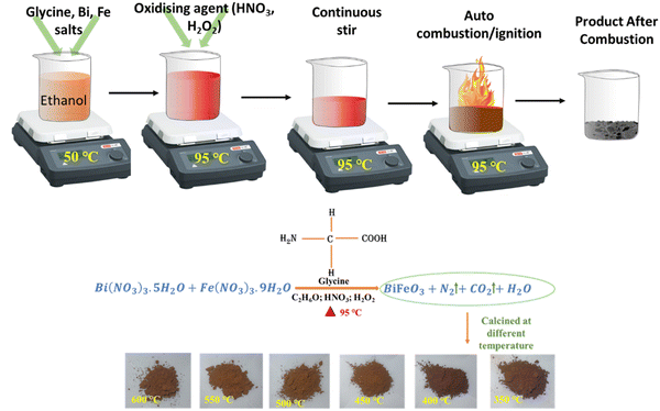
Again, 5 ml hydrogen peroxide (H2O2) is added to this solution, and the observed clear brown color solution is subjected to constant stirring at 95 °C for at least 2–3 hours. Here, H2O2 enhances the reaction kinetics by increasing the reactivity of the fuel mixture by decreasing the ignition time.23 As Akpan et al. have explained, an increase in the heat combustion process is observed for ethanol based solutions by adding H2O2 to them.24 Finally, the solution is converted to a brown color gel, and after a few minutes, the auto-combustion process starts converting it into a dark brown gel and then to deep brown fine nanoparticle powders. This dry fine powder is finally calcinated at different temperatures (TCalcination = 350 °C, 400 °C, 450 °C, 500 °C, 550 °C, and 600 °C) for 2 hours. Fig. 1 presents schematically the synthesis process and the associated chemical reaction for BiFeO3 nanoparticles together with an optical image of the final product at different calcination temperatures.
Characterization of the BiFeO3 nanoparticles
The phase purity and structural parameters of the different temperature calcinated BFO nanoparticles are analyzed using a powder X-ray diffractometer (Bruker D8 Advanced X-ray diffractometer with Cu Kα source, λ = 1.5406 nm). The morphology and composition are investigated using field effect scanning electron microscopy (FESEM) measurements (Thermo Fisher, German), and energy dispersive X-ray (EDX) analysis. Thermogravimetry (TGA) (PerkinElmer make STA 6000 model) analysis is performed from 30 °C to 900 °C under a N2 gas environment with a slow heating rate. The present functional groups are confirmed using Fourier transfer infrared (FTIR) spectroscopy measurement (Bruker Vertex 70V model FTIR system) in transmittance and reflectance modes. The room temperature Raman measurements were carried out with a 532 nm laser beam using a Bayspec spectrograph (NomadicTM). The UV-Vis spectroscopy measurements were carried out using a Cary 4000 spectrometer in diffuse reflectance mode, where the BaSO4 reference sample is used for background correction.Results and discussion
Structural and microstructural study
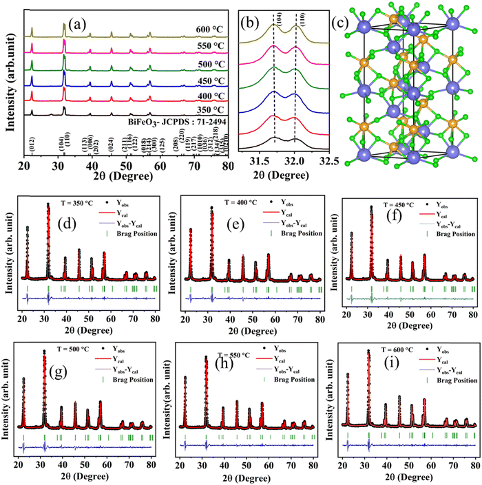
Bismuth ferrite (BiFeO3) nanoparticles are synthesized using the sol–gel auto combustion technique and calcined at six different temperatures (350 °C, 400 °C, 450 °C, 500 °C, 550 °C, and 600 °C). The X-ray diffractograms for all BiFeO3 samples are shown in Fig. 2(a). The observed diffraction peaks at 2θ – 22.387°, 31.725°, 32.010°, 37.588°, 38.938°, 39.413°, 45.690°, 50.278°, 51.260°, 51.643°, 56.334°, 56.873°, 57.052°, 60.597°, 66.278°, 66.931°, 69.630°, 69.950°, 70.599°, 71.234°,71.550°, 75.507°, 75.971°, 79.230°, and 79.622° are indexed in the XRD plot for the rhombohedral distorted structure with the R3c space group. These are consistent with the ICDD PDF #71-2494, and the corresponding reference lines are plotted and indexed with the respective miller indices, Fig. 2(a). However, an additional secondary peak/parasitic phase is observed for a 350 °C annealed BFO sample, which disappears with increasing annealing temperature. Fig. 2(b) shows the (104) and (110) XRD peaks shifting to lower angles with increasing annealing temperature. Here, splitting the (104) and (110) peaks correspond to the rhombohedral distortion in BiFeO3. The XRD patterns for all the samples are refined using the Rietveld refinement process (Fullprof Suite tool), and Fig. 2(c) shows the crystal structure of BiFeO3 in a hexagonal lattice structure, as estimated after the Rietveld refinement of the XRD plots. Fig. 2(d)–(i) shows the XRD refined plots for different temperature annealed samples. The lattice parameters and atomic position for all the samples are extracted from the refinement data and are summarized in Table S1 (ESI†), together with the residual values for the weighed pattern (Rwp, Rp) and goodness of fit (χ2). Furthermore, the rhombohedral lattice parameters (arh and αrh) are computed from the hexagonal lattice parameters extracted from the refinement data using the following equations:25 | (1) |
 | (2) |
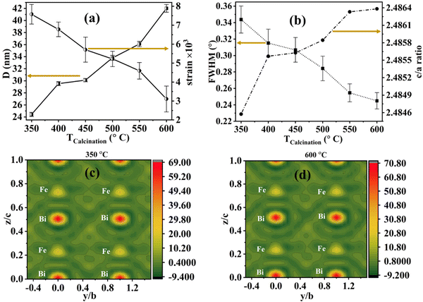
The rhombohedral lattice parameters (arh and αrh) for the 600 °C sample are 5.6353 Å and 59.3417°, well matching the previously reported literature.25 Furthermore, the crystallite size and strain are calculated for these BFO nanoparticles, and these variations against calcination temperature are plotted in Fig. 3(a). The average crystallite size of the NPs can be calculated using the Scherrer formula,26
 | (3) |
As the calcination temperature of the BFO samples increases, the XRD peaks get sharper with reducing full width at half maxima (FWHM). The variation in FWHM for the (104) diffraction plane and c/a ratio are plotted against the calcination temperature in Fig. 3(b). Furthermore, this FWHM is used for estimating the crystallite size (D) and lattice strain (ε) of these different temperature-annealed BFO nanoparticles.27 The modified W–H equation is also used to calculate the D and ε by fitting the curve of (dhkl × βhkl × cos![[thin space (1/6-em)]](https://www.rsc.org/images/entities/char_2009.gif) θ)2versus d2hkl × βhkl × cos
θ)2versus d2hkl × βhkl × cos![[thin space (1/6-em)]](https://www.rsc.org/images/entities/char_2009.gif) θ, where all the parameters are extracted from the refinement data (shown in Fig. S1, ESI†). We observed that the lattice strain decreases with increasing annealing temperature. The lattice strain for the BiFeO3 nanoparticles decreases from 0.00758 to 0.00311. The reduction of the unit cell volume with decreasing average crystallite size leads to an increase in lattice strain inside the unit cell. The measured crystallite size and lattice strain values are in agreement with the reported literature.28 The electron density (ED) maps for the BiFeO3 nanoparticles are measured for different-size BFO nanoparticles from the Rietveld refinement data. It is calculated from the Refinement data using reverse Fourier Transfer calculation based on the correlation of electron scattering density as
θ, where all the parameters are extracted from the refinement data (shown in Fig. S1, ESI†). We observed that the lattice strain decreases with increasing annealing temperature. The lattice strain for the BiFeO3 nanoparticles decreases from 0.00758 to 0.00311. The reduction of the unit cell volume with decreasing average crystallite size leads to an increase in lattice strain inside the unit cell. The measured crystallite size and lattice strain values are in agreement with the reported literature.28 The electron density (ED) maps for the BiFeO3 nanoparticles are measured for different-size BFO nanoparticles from the Rietveld refinement data. It is calculated from the Refinement data using reverse Fourier Transfer calculation based on the correlation of electron scattering density as  . Here, ρ(x, y, z) refers to the electron scattering density, Fhkl refers to the structure factor for various planes denoted by Miller indices (hkl), and V is the total volume of the unit cell.29,30 The contour maps of electron density distributions in the (0, y, z) directions, i.e., for the y–z plane with x = 0, are shown in Fig. 3(c) and (d) for 350 and 600 °C calcinated temperatures. The electron density is maximum around the Bi atom for all BFO nanoparticle samples, followed by iron (Fe) and oxygen (O). This is because the maximum number of electrons are present in the Bi atom. Interestingly, overall ED increases with increasing average crystallite size, i.e., calcination temperature. The charge density ρ is 60.00 at the centre of the Bi atom for 350 °C calcinated temperature (for the smallest particle size) and increases to 70.80 for 600 °C calcinated temperature (for the largest particle size BFO nanomaterials).
Furthermore, to understand the morphology of the synthesized BiFeO3 nanoparticles, field effect scanning electron microscopy analysis is carried out. The FESEM images of the BiFeO3 nanoparticles for different annealing temperatures are shown in Fig. 4(a)–(f). The morphology confirms the large agglomeration of nanoparticles for the lower calcinated temperature BFO sample with specific spherical-shaped nanoparticles with increasing calcinated temperature. The morphology shows improved homogeneity and uniform arrangements with increased grain size for BFO samples calcinated at 550 °C and 600 °C. The FESEM image of the BiFeO3 nanoparticles of the 600 °C sample is shown in Fig. S2(a) (ESI†) with inserted atomic % of different compositional elements for the BiFeO3 nanomaterial sample. These elemental compositions substantiate the stoichiometry of the synthesized BiFeO3 nanoparticle samples. The elemental mapping plots are shown in Fig. S2(b)–(d) (ESI†), confirming the presence of a uniform distribution of Bi, Fe, and O elements in the BiFeO3 nanoparticles together with the absence of any impurity elements. The average grain/particulate size for different annealed BFO NP samples is calculated using ImageJ software and the size distribution plots are shown in Fig. 5(a)–(f). The estimated size agrees with the crystallite size, computed from X-ray diffractograms, as shown in Fig. 3.
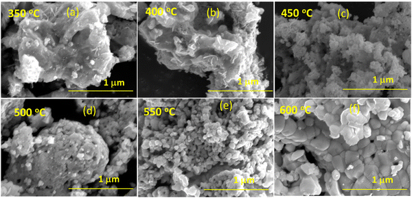 | ||
| Fig. 4 Scanning electron microscope image of BiFeO3 nanoparticles annealed at TCalcination (a) 350 °C, (b) 400 °C, (c) 450 °C, (d) 500 °C, (e) 550 °C, and (f) 600 °C. | ||
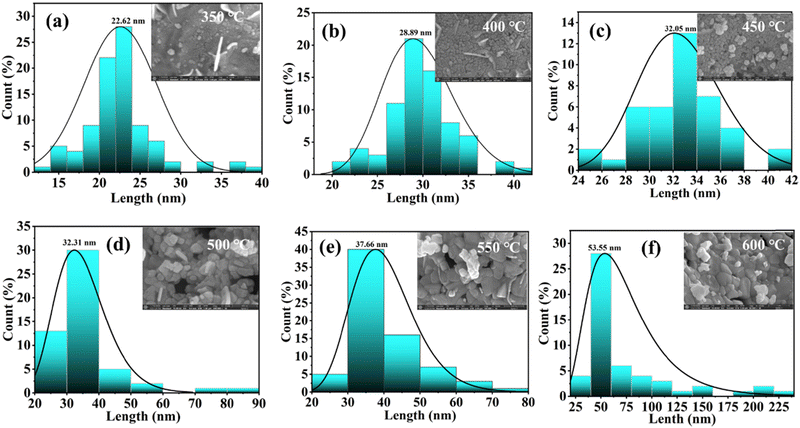 | ||
| Fig. 5 (a–f) Grain size distribution plots for different annealed BiFeO3 nanoparticle samples, showing the average grain size with the inset showing the respective FESEM images. | ||
Thermogravimetry analysis
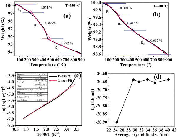
The thermogravimetric analysis is carried out under an N2 atmosphere at a temperature range of 30 °C to 900 °C to investigate the thermodynamical stability of different annealed BiFeO3 nanoparticle samples. Fig. 6(a) and (b) show the TGA plots of BFO NPs annealed at 350 °C and 600 °C. These TGA plots highlight the different degradation regions/paths as R1, R2, and R3. For 350 °C BFO NPs, region R1 corresponds to the weight loss relating to the moisture adsorbed on the sample's surface (∼1.06%), which is only 0.308% for the 600 °C annealed sample. The region R2 around 350 °C and 600 °C corresponds to a weight loss of 3.66% and 0.415%, corresponding to the thermal decomposition of the NO3− compounds. The weight loss is 1.97% and 0.662% for the R3 region, corresponding to the release of CO2 in the thermal decomposition process of (BiO)2CO3. The TGA plots for the remaining BFO-NPs, annealed at different temperatures, are shown in Fig. S3 (ESI†). With increasing temperature, the weight loss decreases continuously due to the rapid decomposition of moisture, nitrates, residual organic compounds, etc., and the formation of crystalline BFO-NPs. The activation energy is calculated for all BFO-NP samples using the Coats–Redfern method31 to investigate the kinetics of the thermal decomposition process.The Coats–Redfern method for the first-order reaction kinetics can be explained as32
 | (4) |
 versus
 plot. For the 350 °C sample, the linear fit curve of
  versus
 is plotted in Fig. 6(c), and the activation energy is calculated using eqn (6). The activation energy (Ea) for the 350 °C BFO-NP sample is ∼−20.900 kJ mol−1. The calculated Ea is shown in Fig. 6(d) for different BFO particle sizes. The activation energy increases with increasing particle size, and the maximum Ea ∼ −20.6362 kJ mol−1 is observed for on average 42 nm BFO nanoparticles.
Optical properties
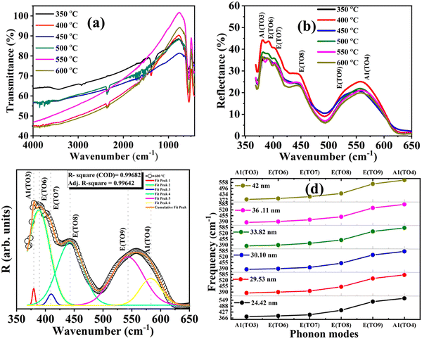
The optical properties of BiFeO3 nanoparticles as a function of different particle sizes were investigated using FTIR, room temperature Raman, and DRS UV-Vis spectroscopy measurements. FTIR measurements were carried out to analyze the possible vibrations originating from different bonds and any variation in these vibrational modes with particle size or strain. Fig. 7(a) shows FTIR spectra for the BiFeO3 NPs in transmission mode. The absorption bands at 445 cm−1 and 545 cm−1 are related to the stretching of Bi–O and bending of Fe–O vibrations, respectively, associated with BiO6 and FeO6 octahedral sites in BiFeO3.33 As the annealing temperature increases, the absorption bands get sharper, showing the high crystallinity of the BiFeO3 NPs. The absorption bands at 2354 cm−1 and 3568 cm−1 correspond to CO2 modes and O–H stretching vibrations, attributed to the absorption of organic precursors at the surface, and these vanish almost with increasing the annealing temperature.34 We also measured the reflectance for different BFO nanoparticles, shown in Fig. 7(b), for different temperature-annealed BFO nanoparticle samples. Here, changes in infrared active phonon modes are investigated for the different temperature-annealed BFO nanoparticle samples. According to Group theory analysis at the Γ point, R3c-BiFeO3 possesses several phonon modes, described as35| Γ(R3c) = 4AIR,R1 ⊕ 9EIR,R ⊕ 5A2 | (5) |
The frequency of six transverse modes shows a redshift with decreasing BFO nanoparticle size. The E(TO7) and A1(TO4) modes for BFO nanoparticle samples with 42 nm particle size are observed to be around 14 cm−1 higher than those of 24.42 nm BFO-NPs. The variations in all of the observed six IR active modes are plotted in Fig. 7(d) for different size BFO NPs. The plots show the increase in the wavenumber of different IR phonon modes with increasing the particle size. The details of IR active vibrational modes are listed in Table S3 (ESI†) for different BFO-NP samples.
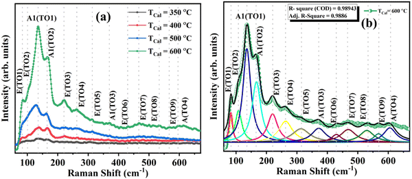
These FTIR studies are compensated with the room temperature Raman measurements on these different temperature annealed BiFeO3 nanoparticle samples to further infer lattice properties, spin–phonon coupling, structural phase, bond length variation, and bond angle in these materials.39 The Raman spectrum is shown in Fig. 8(a) for TCalcination = 350, 400, 500 and 600 °C, and the spectrum for TCalcination = 600 °C is fitted for possible vibrational peaks (Fig. 8(b)). Here, the Raman spectrum is fitted with the Lorentzian distribution function given by 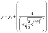 . The fitted spectrum for all other samples is provided in Fig. S4 (ESI†). There are a total of 13 Raman active modes in the BiFeO3-R3c phase, as represented by the irreducible representation in eqn (5). The crystallinity of the synthesized BFO NP samples increases with increasing calcination temperature and thus, the mode intensity becomes larger. That's why we opted for the Raman spectrum for the 600 °C annealed BFO nanoparticle sample and all 13 Raman active modes are fitted for distinguishing them clearly. All the 13 Raman active modes, i.e., E(TO1); (83.78 cm−1), E(TO2); (108.23 cm−1), A1(TO1); (136.49 cm−1), E(TO3); (166.90 cm−1), E(TO4); (220.05 cm−1), A1(TO2); (262.55 cm−1), E(TO5); (313.18 cm−1), A1(TO3); (371.69 cm−1), E(TO6); (429.60 cm−1), E(TO7); (468.62 cm−1), E(TO8); (529.77 cm−1), E(TO9); (568.03 cm−1), A1(TO4); (605.13 cm−1) are clearly distinguishable, suggesting the formation of highly phase pure R3c-BiFeO3 nanoparticles. The intensity of the Raman modes increases with increasing calcination temperature, and this is attributed to (i) enhanced crystallinity and (ii) the resonance with laser excitation matching with the electronic absorption bands in the BiFeO3 nanoparticles.40,41 The observed vibrational modes are also in agreement with the reported literature.39,42,43 Table S4 (ESI†) lists all the fitted Raman modes for the 350, 400, 500, and 600 °C annealed BiFeO3 nanoparticle samples.
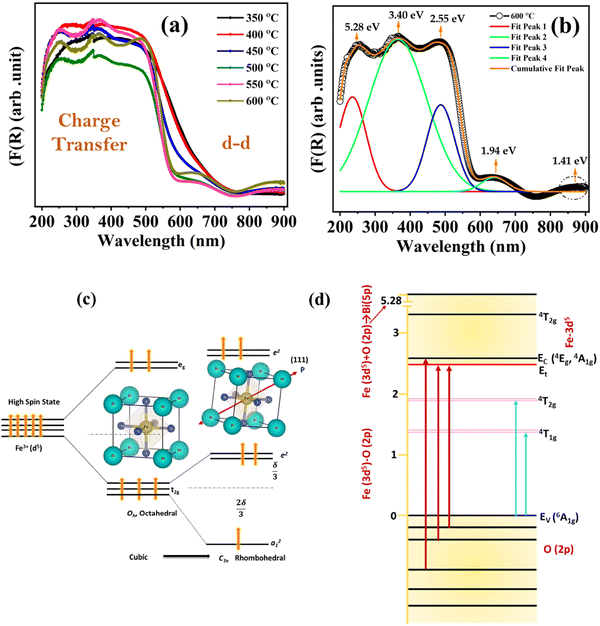
UV-visible spectroscopy measurements were carried out in the 200–900 nm wavelength range to get further insight into the various electronic transitions in BiFeO3 NPs. The optical band gap of the BFO nanoparticles is characterized using diffuse reflectance UV-visible spectroscopy measurements. The reflectance versus wavelength plots for different annealed BFO-NPs are shown in Fig. S5 (ESI†). The broad bands near the wavelength ∼600 nm move towards lower wavelength/higher energy as the particle size increases. The absorption spectra of the BFO NPs are studied through the Kubelka–Munk function given by,
 | (6) |
 .48 This value is consistent with the X-ray photoelectron spectroscopy measurements on the BiFeO3 system.44,46 Additionally, two more absorption bands are observed at ∼1.41 eV and 1.95 eV (doubly degenerate), corresponding to 6A1g–4T1g and 6A1g–4T2g transitions, respectively. In Fig. 9(c), the crystal field symmetry breaking of cubic Oh to rhombohedral C3V is shown schematically. The schematic of the electronic energy level diagram of BiFeO3 nanoparticles is shown in Fig. 9(d), where EV and EC correspond to the top of the valence band and the bottom of the conduction band, and Et refers to the defect state. The above-mentioned inter-electronic transitions are levelled schematically in Fig. 9(d). We observed 1.41 eV d–d on sight transitions for all samples except for the 350 °C BFO NPs (Fig. S6(f), ESI†). The p–d charge transfer bands shift towards higher energy and d–d on sight transitions, i.e., 6A1g → 4T1g and 6A1g → 4T2g shift to lower energy with decreasing BFO nanoparticle size (summarized in Table 1). The similar blue shift characteristics for the p–d charge transfer band with reduced BiFeO3 nanoparticle size are also reported in the literature.43 Hence, as the unit cell volume decreases, the chemical pressure inside the lattice increases, leading to a red shift in the d–d transition bands, satisfying the modified Tanabe–Sugamo diagram.49–51
| T Calcination (°C) | Charge transfer bands (eV) | d–d transition (eV) | ||
|---|---|---|---|---|
| 350 | 5.709 (±0.160) | 3.659 (±0.160) | 2.415 (±0.130) | 1.858 (±0.120) |
| 400 | 5.471 (±0.018) | 3.559 (±0.025) | 2.436 (±0.037) | 1.914 (±0.009) |
| 450 | 5.451 (±0.018) | 3.489 (±0.008) | 2.463 (±0.002) | 1.954 (±0.005) |
| 500 | 5.413 (±0.011) | 3.412 (±0.011) | 2.488 (±0.002) | 1.929 (±0.008) |
| 550 | 5.360 (±0.022) | 3.328 (±0.008) | 2.498 (±0.002) | 1.919 (±0.006) |
| 600 | 5.279 (±0.036) | 3.401 (±0.012) | 2.545 (±0.014) | 1.938 (±0.007) |
Furthermore, Tauc's formula, i.e., αhν = A(hν − Eg)n, is used to determine the exact band gap values of these BFO nanoparticle samples. Here, α is the absorption coefficient, Eg is the band gap, and n takes the value 2 or  depending upon the indirect or direct band transitions inside the material. Fig. 10(a) and (b) show the Tauc plots and variation for the direct band gap for different BFO NPs. The optical band gap (Eg) can be estimated by extrapolating the Tauc plot to zero for (αhν)2 (Fig. 10(a)). We observed an increase in Eg values with increasing average crystallite size or annealing temperature, as shown in Fig. 10(b). The band gap increases from 1.93 eV to 2.22 eV, increasing the particle size from 24.42 nm to 42 nm. The reduction in band gap with decreasing NP size contradicts the quantum confinement effect (QCE), supporting the earlier reported studies in the bismuth ferrite, and CuO NP systems.52,53
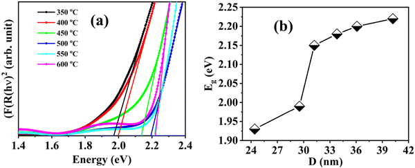 | ||
| Fig. 10 (a) Tauc plot to estimate the direct band gap and (b) the variation of optical band gap with average particle size for different annealed BiFeO3 nanoparticle samples. | ||
These observed band gap values are less than the reported bulk BFO band gap.46,54 This unusual trend in the variation in Eg values is attributed to the strain-modulated band gap engineering in the BFO nanoparticles. The strain-induced changes become dominant over the particle size effect in these strongly correlated systems and are consistent with the reported literature.43 Additionally, the reduction in particle size increases the density of the particles as the volume reduces drastically, thus giving rise to the large strain effect.51 This large strain may give rise to shallow energy levels between the conduction band and the valence band, reducing the band gap (Eg) for smaller particles.
Conclusion
Bismuth ferrite multiferroic nanoparticles are synthesized using a sol–gel auto-combustion method followed by controlled post-annealing at different temperatures, and the effect of the BiFeO3 nanoparticles’ size is investigated on the structural, microstructural, and optical properties. The 600 °C annealed BFO sample shows a highly crystalline 42 nm particle size. The room temperature Raman measurements confirm the presence of all the 13 Raman modes in the sample with 6 IR active phonon modes at frequency ranges 0 to 700 cm−1 and 380 to 650 cm−1, respectively. With increasing particle size, the phonon modes show a redshift. The diffuse reflectance spectroscopy measurements confirm the presence of various absorption bands in the K–M plot. The size of the BFO nanoparticles affects the band gaps and the crystal field splitting; as a result, the energies of different interband transitions change. This study shows the path of engineering materials properties using strain modulation with a large tunability on the bandgap values, indicating the inverse quantum confinement trend, where the impact of strain supersedes the size effect.Conflicts of interest
The authors declare no competing interests for this work.Acknowledgements
Author Ambesh Dixit acknowledges SERB, DST, Government of India through projects SERB/F/10090/2021-2022 and #CRG/2020/004023 for supporting this work. Author Priyambada Sahoo acknowledges DST, Inspire Fellowship #DST/INSPIRE/03/2019/001452, Government of India. She also acknowledges Dr Vijay K Singh, Dr Anant Prakash Panday, Mr Abhijeet J Kale, Mr Sumit Kukreti, Mr Chandra Prakash, Ms Surbhi Ramawat, Ms Bharti Rani, Ms Priyanka Saini, Ms Minakshi Sharma, Mr Jitendra K Yadav, Mr Piyush Choudhary, Mr Ankit Yadav, Mr Biswajit Pal, and Mr Sunil Batesar for their support throughout the work.References
- S. J. Clark and J. Robertson, Appl. Phys. Lett., 2007, 90, 1–4 CrossRef.
- M. Fiebig, J. Phys. D: Appl. Phys., 2005, 38, R123–R152 CrossRef CAS.
- G. L. Yuan, S. W. Or, H. L. W. Chan and Z. G. Liu, J. Appl. Phys., 2007, 101, 24106 CrossRef.
- A. Sundaresan and N. V. Ter-Oganessian, J. Appl. Phys., 2021, 129, 60901 CrossRef CAS.
- G. W. T. Kieliba, S. Bau, R. Schober, D. OBwald, S. Reber and A. Eyer, Sol. Energy Mater. Sol. Cells, 2002, 74, 261–266 CrossRef.
- S. Xu, J. Qiu, T. Jia, C. Li, H. Sun and Z. Xu, Opt. Commun., 2007, 274, 163–166 CrossRef CAS.
- A. Kumar Sinha, Mater. Today Proc., 2020, 42, 1519–1521 CrossRef.
- R. Ramesh and N. A. Spaldin, Nanosci. Technol. A Collect. Rev. Nat. Journals, 2009, 3, 20–28 Search PubMed.
- C. Ederer and N. A. Spaldin, Phys. Rev. B: Condens. Matter Mater. Phys., 2005, 71, 1–4 Search PubMed.
- A. K. Sinha, B. Bhushan, Jagannath, N. Gupta, S. Sen, C. L. Prajapat, J. Nuwad, P. Bhatt, S. K. Mishra, S. S. Meena and A. Priyam, Solid State Sci., 2020, 102, 106168 CrossRef CAS.
- J. R. Teague, R. Gerson and W. J. James, Solid State Commun., 1970, 8, 1073–1074 CrossRef CAS.
- C. Ederer and N. A. Spaldin, Curr. Opin. Solid State Mater. Sci., 2005, 9, 128–139 CrossRef CAS.
- S. R. Basu, L. W. Martin, Y. H. Chu, M. Gajek, R. Ramesh, R. C. Rai, X. Xu and J. L. Musfeldt, Appl. Phys. Lett., 2008, 92, 91905 CrossRef.
- A. J. Hauser, J. Zhang, L. Mier, R. A. Ricciardo, P. M. Woodward, T. L. Gustafson, L. J. Brillson and F. Y. Yang, Appl. Phys. Lett., 2008, 92, 1–4 Search PubMed.
- F. Gao, X. Chen, K. Yin, S. Dong, Z. Ren, F. Yuan, T. Yu, Z. Zou and J. M. Liu, Adv. Mater., 2007, 19, 2889–2892 CrossRef CAS.
- S. Y. Yang, L. W. Martin, S. J. Byrnes, T. E. Conry, S. R. Basu, D. Paran, L. Reichertz, J. Ihlefeld, C. Adamo, A. Melville, Y. H. Chu, C. H. Yang, J. L. Musfeldt, D. G. Schlom, J. W. Ager and R. Ramesh, Appl. Phys. Lett., 2009, 95, 93–96 Search PubMed.
- H. Kimura, S. Kobayashi, S. Wakimoto, Y. Noda and K. Kohn, Ferroelectrics, 2007, 354, 77–85 CrossRef CAS.
- K. Saito and K. Kohn, J. Phys.: Condens. Matter, 1995, 7, 2855–2863 CrossRef CAS.
- T. Kimura, T. Goto, H. Shintani, K. Ishizaka, T. Arima and Y. Tokura, Nature, 2003, 426, 55–58 CrossRef CAS PubMed.
- R. V. Pisarev, A. S. Moskvin, A. M. Kalashnikova and T. Rasing, Phys. Rev. B: Condens. Matter Mater. Phys., 2009, 79, 1–16 CrossRef.
- M. A. Wahba, S. M. Yakout, A. M. Youssef, W. Sharmoukh, A. M. E. Sayed and M. S. Khalil, J. Supercond. Nov. Magn., 2022, 35, 3689–3704 CrossRef CAS.
- A. Varma, A. S. Mukasyan, A. S. Rogachev and K. V. Manukyan, Chem. Rev., 2016, 116, 14493–14586 CrossRef CAS PubMed.
- B. Gribi, Y. Lin, X. Hui, C. Zhang and C. J. Sung, Fuel, 2018, 223, 324–333 CrossRef CAS.
- I. A. Akpan and B. R. Abiona, J. Theor. Appl. Phys., 2012, 31, 83–92 Search PubMed.
- A. Dubey, M. Escobar Castillo, J. Landers, S. Salamon, H. Wende, U. Hagemann, P. Gemeiner, B. Dkhil, V. V. Shvartsman and D. C. Lupascu, J. Phys. Chem. C, 2020, 124, 22266–22277 CrossRef CAS.
- A. Monshi, M. R. Foroughi and M. R. Monshi, World J. Nano Sci. Eng., 2012, 02, 154–160 CrossRef.
- V. Mote, Y. Purushotham and B. Dole, J. Theor. Appl. Phys., 2012, 6, 2–9 CrossRef.
- E. Ramos, A. Cardona-Rodríguez, D. Carranza-Celis, R. González-Hernández, D. Muraca and J. G. Ramírez, J. Phys.: Condens. Matter, 2020, 32, 185703 CAS.
- S. Chaturvedi, P. Shyam, A. Apte, J. Kumar, A. Bhattacharyya, A. M. Awasthi and S. Kulkarni, Phys. Rev. B, 2016, 93, 1–12 CrossRef.
- S. Chauhan, M. Kumar, H. Pandey, S. Chhoker and S. C. Katyal, J. Alloys Compd., 2019, 811, 151965 CrossRef CAS.
- J. M. Rami, C. D. Patel, C. M. Patel and M. V. Patel, Mater. Today Proc., 2020, 43, 655–659 CrossRef.
- S. K. Paswan, S. Kumari, M. Kar, A. Singh, H. Pathak, J. P. Borah and L. Kumar, J. Phys. Chem. Solids, 2021, 151, 109928 CrossRef CAS.
- X. Shi, S. Quan, L. Yang, C. Liu and F. Shi, J. Mater. Sci., 2019, 54, 12424–12436 CrossRef CAS.
- J. L. Ortiz-Quiñonez, D. Díaz, I. Zumeta-Dubé, H. Arriola-Santamaría, I. Betancourt, P. Santiago-Jacinto and N. Nava-Etzana, Inorg. Chem., 2013, 52, 10306–10317 CrossRef PubMed.
- P. Chen, X. Xu, C. Koenigsmann, A. C. Santulli, S. S. Wong and J. L. Musfeldt, Nano Lett., 2010, 10, 4526–4532 CrossRef CAS PubMed.
- S. Kamba, D. Nuzhnyy, M. Savinov, J. Šebek, J. Petzelt, J. Prokleška, R. Haumont and J. Kreisel, Phys. Rev. B: Condens. Matter Mater. Phys., 2007, 75, 1–7 CrossRef.
- P. Hermet, M. Goffinet, J. Kreisel and P. Ghosez, Phys. Rev. B: Condens. Matter Mater. Phys., 2007, 75, 3–6 CrossRef.
- B. K. Das, B. Ramachandran, A. Dixit, M. S. Ramachandra Rao, R. Naik, A. T. Sathyanarayana, T. N. Sairam and G. Amarendra, J. Alloys Compd., 2020, 832, 154754 CrossRef CAS.
- D. Carranza-Celis, A. Cardona-Rodríguez, J. Narváez, O. Moscoso-Londono, D. Muraca, M. Knobel, N. Ornelas-Soto, A. Reiber and J. G. Ramírez, Sci. Rep., 2019, 9, 1–9 CrossRef CAS PubMed.
- J. Wang, L. Luo, C. Han, R. Yun, X. Tang, Y. Zhu, Z. Nie, W. Zhao and Z. Feng, Materials, 2019, 12, 1444 CrossRef CAS PubMed.
- S. Lohumi, M. S. Kim, J. Qin and B.-K. Cho, Sensors, 2019, 19, 2698 CrossRef CAS PubMed.
- T. D. Rao, T. Karthik and S. Asthana, J. Rare Earths, 2013, 31, 370–375 CrossRef CAS.
- P. S. V. Mocherla, C. Karthik, R. Ubic, M. S. Ramachandra Rao and C. Sudakar, Appl. Phys. Lett., 2014, 105, 132409 CrossRef.
- X. Bai, J. Wei, B. Tian, Y. Liu, T. Reiss, N. Guiblin, P. Gemeiner, B. Dkhil and I. C. Infante, J. Phys. Chem. C, 2016, 120, 3595–3601 CrossRef CAS.
- M. O. Ramirez, A. Kumar, S. A. Denev, N. J. Podraza, X. S. Xu, R. C. Rai, Y. H. Chu, J. Seidel, L. W. Martin, S. Y. Yang, E. Saiz, J. F. Ihlefeld, S. Lee, J. Klug, S. W. Cheong, M. J. Bedzyk, O. Auciello, D. G. Schlom, R. Ramesh, J. Orenstein, J. L. Musfeldt and V. Gopalan, Phys. Rev. B: Condens. Matter Mater. Phys., 2009, 79, 1–9 Search PubMed.
- B. Ramachandran, A. Dixit, R. Naik, G. Lawes and M. S. R. Rao, Phys. Rev. B: Condens. Matter Mater. Phys., 2010, 82, 1–4 CrossRef.
- X. S. Xu, T. V. Brinzari, S. Lee, Y. H. Chu, L. W. Martin, A. Kumar, S. McGill, R. C. Rai, R. Ramesh, V. Gopalan, S. W. Cheong and J. L. Musfeldt, Phys. Rev. B: Condens. Matter Mater. Phys., 2009, 79, 4–7 Search PubMed.
- X. Bai, J. Wei, B. Tian, Y. Liu, T. Reiss, N. Guiblin, P. Gemeiner, B. Dkhil and I. C. Infante, J. Phys. Chem. C, 2016, 120, 3595–3601 CrossRef CAS.
- S. Gómez-Salces, F. Aguado, F. Rodríguez, R. Valiente, J. González, R. Haumont and J. Kreisel, Phys. Rev. B: Condens. Matter Mater. Phys., 2012, 85, 1–9 CrossRef.
- B. Ramachandran and M. S. Ramachandra Rao, J. Appl. Phys., 2012, 112, 73516 CrossRef.
- S. Hussain and S. K. Hasanain, J. Alloys Compd., 2016, 688, 1151–1156 CrossRef CAS.
- P. S. V. Mocherla, C. Karthik, R. Ubic, M. S. Ramachandra Rao and C. Sudakar, Appl. Phys. Lett., 2013, 103, 022910 CrossRef.
- P. Sahoo, M. J. Sneha, B. P. Mandal and A. Dixit, Mater. Lett., 2022, 324, 132747 CrossRef CAS.
- G. Catalan and J. F. Scott, Adv. Mater., 2009, 21, 2463–2485 CrossRef CAS.
Footnote |
| † Electronic supplementary information (ESI) available. See DOI: https://doi.org/10.1039/d3cp05267b |
| This journal is © the Owner Societies 2024 |

