 Open Access Article
Creative Commons Attribution 3.0 Unported Licence
An intrinsic electrical conductivity study of perovskite powders MAPbX3 (X = I, Br, Cl) to investigate its effect on their photovoltaic performance†
Shafi Ullah *a,
Andreu Andriob,
Julia Marí-Guaitaa,
Hanif Ullahc,
Antonio Méndez-Blasd,
Roxana M. del Castillo Vázquez
 e,
Bernabé Maria and
Vicente Compañ
 *f
*f
aInstituto de diseño y Fabricación (IDF), Universitat Politècnica de València (UPV), Camino de Vera, s/n, 46022 Valencia, Spain. E-mail: Shafi399@yahoo.com
bDepartamento de Física Aplicada, Universitat Jaume I, Avda. Sos Baynat, s/n, 12080-Castellón de la Plana, Spain
cDepartment of Electrical Engineering, Federal Urdu University (FUUAST), Islamabad, Pakistan
dInstituto de Física, Benemérita Universidad Autónoma de Puebla, Apartado Postal J-48, Puebla, 72570, Mexico
eDepartamento de Física, Facultad de Ciencias, Universidad Nacional Autónoma de México (UNAM), DF, Mexico
fDepartamento de Termodinámica Aplicada (ETSII), Universitat Politècnica de València, Camino de Vera s/n, 46022 Valencia, Spain. E-mail: vicommo@ter.upv.es
First published on 7th February 2024
Abstract
An investigation into the intrinsic electrical conductivity of perovskite powders MAPbX3, where X represents iodine (I), bromine (Br), or chlorine (Cl), was conducted to explore its impact on their photovoltaic performance. Results revealed that MAPbCl3 demonstrated light absorption ability in the ultraviolet and visible regions, while MAPbBr3 showed capacity for light absorption at longer wavelengths in the visible spectrum. On the other hand, MAPbI3 exhibited good absorption at longer wavelengths, indicating its ability to absorb light in the near-infrared region. The optical bandgap of each perovskite was determined to be 2.90 eV for MAPbCl3, 2.20 eV for MAPbBr3, and 1.47 eV for MAPbI3. The electrical conductivities of these powders were measured in-plane using the four-probe method and through-plane by electrochemical impedance spectroscopy (EIS). Electrochemical impedance spectroscopy (EIS) studies revealed a significant change in the conductivity of the MAPbI3 perovskite at temperatures between 80 °C and 100 °C. This change could be attributed to structural modifications induced when the temperature exceeds these values. The through-plane conductivity changed from 3 × 10⁻⁸ S cm−1 at 60 °C to approximately 6 × 10⁻⁵ S cm−1 at 120 °C and around 2 × 10⁻³ S cm−1 at 200 °C. Meanwhile, the sheet conductivity (in-plane conductivity) measurements performed at ambient temperature reveal that sheet conductivities are 489 × 103 S m−1, 486 × 103 S m−1 and 510 × 103 S m−1 for MAPbBr3, MAPbCl3 and MAPbI3, respectively. This study provides valuable insights for optimizing the performance of perovskite solar cells. Understanding how dopants influence the electrical conductivity and photovoltaic properties of the perovskite material, this work will enable researchers to design and engineer more efficient and stable solar cell devices based on MAPbX3 perovskites.
1. Introduction
Over the past few years, there has been a remarkable advancement in optoelectronic devices utilizing hybrid organic/inorganic halide perovskites as active semiconductor materials.1–3 Specifically, perovskite-based solar cells (PSCs) have achieved impressive efficiencies, reaching 25.2%, comparable to traditional silicon-based solar cells.4 Additionally, there have been continuous improvements in the stability of these devices, indicating their potential for commercialization.5,6 Despite the enthusiasm surrounding halide perovskites, their versatile processing methods, such as solution-based or evaporation techniques, are more complex compared to those used for organic semiconductors. The reason for this complexity lies in the close coupling between the actual crystallization of the perovskite material and its film formation. These two processes occur simultaneously and need to be optimized in parallel. This coupling contributes to the challenge of achieving consistent film formation and results in significant variations in device performance, even within the same laboratory. Such inconsistencies hinder the industrial adoption of perovskite-based devices.7Addressing these challenges and improving the reproducibility of film formation are essential steps towards the widespread adoption of perovskite-based optoelectronic devices in commercial applications. By better understanding and controlling the crystallization and film formation processes, researchers can enhance the performance and reliability of perovskite-based devices, ultimately paving the way for their successful integration into the market. Furthermore, the versatility of organic–inorganic hybrid perovskites extends beyond their impressive efficiencies, as their structural and optoelectronic characteristics can be readily adjusted through compositional engineering involving diverse organic ligands, metals, or halogens. This compositional variability has allowed researchers to utilize perovskites with different bandgap energies (Eg) in various applications, including wave-tunable lasing and light-emitting diodes.8,9 Moreover, these tunable compositions have proven to be highly efficient in solar cell technology. Nevertheless, it is crucial to consider that the lattice of perovskites is highly sensitive to the size of coordinating organic cations. In cases where the cations are excessively large, two-dimensional (2D) layered perovskites with distinct semiconducting properties are formed.10,11
An alternative method for synthesizing halide perovskite powders, which does not involve the formation of layers, is the mechanochemical synthesis. Researchers have successfully demonstrated this procedure for various lead-containing and lead-free halide perovskite compositions.12–15 The use of perovskite powders offers several advantages, such as superior storage stability, when compared to stock solution counterparts.16 Additionally, dry synthesis approaches for perovskite powders expand the range of available reactants, as there are no solubility limitations.17 The precise control of precursor stoichiometry in this method translates to better overall synthesis control, leading to improved device properties when converting the prepared perovskite powders into solution-based thin-films.18–20 Moreover, the potential of halide perovskite powders is showcased in the demonstration of efficient X-ray detectors. These detectors were achieved by directly processing solution-based perovskite powders into a thick layer without the use of solvents, highlighting the versatility of these materials.21
The mechanochemical synthesis of perovskite powders shows promise, but there is still a lack of detailed understanding regarding the relationship between the properties of reactants, synthesis parameters, and the resulting structural and optoelectronic properties of the final perovskite powders. To address this gap, our study focuses on investigating two crucial aspects: the intrinsic conductivity of the mechanochemically synthesized perovskite powders and their ability to withstand external stress factors, such as temperature variations and frequency changes. These characteristics are significant when considering the potential commercial deployment of this synthesis method. By gaining insights into the conductivity and resilience of perovskite powders, we aim to shed light on their suitability and reliability for various practical applications.
In this regard, our research will primarily focus on studying the conductivity of perovskite powders of MAPbX3, where X = I, Br and Cl, to understand how it affects the photovoltaic performance of these materials. To achieve this goal, we conducted in-plane conductivity measurements to determine the sheet resistivity of the perovskites and through-plane conductivity measurements by EIS to quantify the transversal conductivity.
In previous studies of our group, broadband dielectric spectroscopy has been employed to investigate the relationship between diffusivity, charge carrier density, and Debye length in relation to the structural dynamics of SILLPs.22–24 Following a similar procedure, in this investigation, the influence of electrode polarization (EP) has been taken into account using a single Debye relaxation model, as demonstrated in the analysis conducted by Trukhan,25 Sorensen et al.,26 and MacDonald.27–29 Following the same line of research as other researchers,30–34 in this work, by incorporating the EP approach and fitting the peaks corresponding to the maximum of tan![[thin space (1/6-em)]](https://www.rsc.org/images/entities/char_2009.gif) δ, we were able to determine the diffusivity, the mobility and charge carrier density of the various doping agents within the perovskite structure. These parameters provided insights into the cumulative process occurring in the system, resulting from interactions between charge carriers and mobile ions in the perovskites. From conductivity measurements, we will provide valuable insights into the behavior of the perovskite materials and its potential impact on enhancing their photovoltaic performance.
δ, we were able to determine the diffusivity, the mobility and charge carrier density of the various doping agents within the perovskite structure. These parameters provided insights into the cumulative process occurring in the system, resulting from interactions between charge carriers and mobile ions in the perovskites. From conductivity measurements, we will provide valuable insights into the behavior of the perovskite materials and its potential impact on enhancing their photovoltaic performance.
2. Experimental section
2.1. Synthesis of MAPbX3 (X = I, Br, Cl) powders
All the starting materials were purchased from Sigma Aldrich and used as received without further purification. Perovskite crystal powders were synthesized by mixing an equimolar ratio of 0.30 mol CH3NH2 (33% in methanol) and the corresponding hydro halide acid HX (X = I, Br, Cl). The mixture was stirred for 2 hours in a 250 mL round-bottom flask, and the flask was kept in an ice bath at 0 °C. Subsequently, the mixture was heated to 100 °C for 30 minutes. A solution of 0.03 mol of Pb(NO3)2, previously dissolved in 50 mL of distilled water, was added dropwise to the hot MAX3 (X = I, Br, Cl) solution under vigorous stirring.Following this process, a precipitate of crystalline powders formed, exhibiting different colors: black for iodide, orange for bromide, and white for chloride. The remaining solution was allowed to cool to 50 °C and then filtered. The resulting crystalline powders were washed multiple times with absolute ethanol and diethyl ether. Finally, the powders were dried in an electric oven at 100 °C for 24 hours and then stored in a vacuum for further characterization.
The crystallographic properties of the synthesized samples were analyzed using X-ray diffraction (XRD) with a Rigaku Ultima IV diffractometer. Cu-Kα radiation with a wavelength (λ) of 1.5406 Å was used, and the measurements were conducted in the 2θ range from 10° to 60°, with a step size of 0.02°. For the examination of the sample's microstructure, transmission electron microscopy (TEM) measurements were carried out using a JEO-JEM-1010 instrument at 2.5 kV. To investigate the optical properties of the samples, absorption measurements were performed using an Ocean Optics HR4000 spectrophotometer equipped with a Si-CCD detector. The measurements were taken within the wavelength range of 400 nm to 1000 nm.
2.2. Conductivity measurements
 | (1) |
| ρs = Rs·t | (2) |
Finally, the sheet conductivity (i.e., in-plane conductivity) of perovskites can be obtained from the inverse of the sheet resistivity as
 | (3) |
3. Results and discussion
3.1 XRD analysis
The preparation of perovskite powders of MAPbX3, (X = I, Br, or Cl) was carried out as described above in the experimental section. These perovskite powders exhibit good solubility in polar organic solvents, including N-methyl-2-pyrrolidinone (NMP), N,N-dimethylacetamide (DMAC), N,N-dimethylformamide (DMF), and dimethyl sulfoxide (DMSO). In Fig. 1, optical images of the synthesized MAPbX3 perovskite powders are presented, along with their corresponding X-ray diffraction (XRD) spectra. The colors of the synthesized powders are observed as follows: black for MAPbI3, bright orange for MAPbBr3, and almost colorless and transparent for MAPbCl3. The XRD spectra exhibit characteristic peaks that align well with those reported in the literature.41–44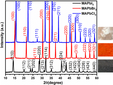 | ||
| Fig. 1 X-ray diffractograms of MAPbX3 (X = I, Br, Cl) along with optical images of perovskite powders. | ||
The XRD analysis highlights that the three halides MAPbX3 share a consistent phase, free from secondary contributions like MAX or PbX2. Notably, MAPbI3 adopts a tetragonal crystal structure, while the remaining films conform to a cubic perovskite structure. The lattice parameters follow a decreasing sequence of I, Br, and Cl. This results in a distinct shift of the (200) peak towards higher diffraction angles (MAPbI3: 28.70°, MAPbBr3: 30.36°, and MAPbCl3: 31.69°), aligning with both anticipated outcomes and the existing literature. Fig. 1 visually compares the final XRD measurements for the three deposited samples.
Additionally, the powder X-ray diffraction patterns of all three synthesized compounds confirm the presence of phase-pure products. Specifically, MAPbI3 exhibits a tetragonal structure, while both MAPbBr3 and MAPbCl3 crystallize in a cubic structure, as detailed in Table 1. These structures correspond to the room-temperature configurations previously reported for these materials.45 Besides, the quantitative XRD results are supported by TEM and HRTEM characterization.
| System | Space group | Crystal system | a, Å | b, Å | c, Å |
|---|---|---|---|---|---|
| MAPbI3 | I4cm | Tetragonal | 8.819(2) | 8.819(2) | 12.634(5) |
| MAPbBr3 | Pm3m | Cubic | 5.875(8) | 5.875(8) | 5.875(8) |
| MAPbCl3 | Pm3m | Cubic | 5.675(4) | 5.675(4) | 5.675(4) |
3.2 TEM study
Fig. 2 presents the results of High-Resolution Transmission Electron Microscopy (HRTEM) used to closely examine the nanostructures of MAPbX3 (X = I, Br, and Cl) perovskite powders. To conduct the analysis, the powders were dispersed and deposited onto a lacey carbon copper grid. HRTEM images were collected from various areas of the samples, and the findings revealed high crystalline quality, indicating the absence of planar or extended defects in all the studied samples (Fig. 2a–c). In Fig. 2a, an HRTEM image provides an overview of the nanostructure of MAPbI3 perovskite powder. The presence of crystallites with different orientations is clearly visible. In higher electron-transparent regions, well-defined atomic columns are observed. Furthermore, the HRTEM images in Fig. 2a display lattice fringes with a spacing of 0.55 nm, corresponding to the d-spacing (114, 222) planes of the tetragonal MAPbI3 structure. These observations align with previous findings reported in the existing literature.48,49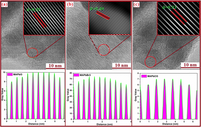 | ||
| Fig. 2 (a)–(c) HR-TEM images of MAPbX3 (X = I, Br and Cl) perovskites along with the corresponding shell layer distance images. | ||
Similarly, Fig. 2b depicts the HRTEM image of the MAPbBr3 perovskite powder, exhibiting a lattice spacing of 0.40 nm, which uniquely matches the interplanar distance of the (200) plane in the cubic MAPbBr3 structure. This finding is consistent with data obtained from XRD experiments.50 Moreover, the HRTEM image of the MAPbCl3 sample in Fig. 2c reveals a separation of 0.90 nm. These results indicate the interplanar distance of the (110) plane in the cubic phase of the MAPbCl3 structure and the (211) plane of the orthorhombic secondary phase of PbCl2.
Overall, the HRTEM analysis of the MAPbX3 perovskite powder samples has provided valuable insights into their nanostructure, crystal quality, and crystallographic information. These findings are essential for a comprehensive understanding of the properties and potential applications of these perovskite materials.
3.3 Optical results
In Fig. 3 the UV-visible spectra of the perovskite powders are displayed to investigate the optoelectronic properties of these materials, revealing distinct absorption onsets for each composition. Specifically, MAPbCl3 exhibits a sharp absorption onset at 427 nm, indicating its ability to absorb light in the ultraviolet and visible regions, while MAPbBr3 shows an absorption onset at 563 nm, showing its capacity to absorb light at longer wavelengths in the visible spectrum. Lastly, for MAPbI3, the absorption onset occurs at a longer wavelength of 843 nm, indicating its ability to absorb light in the near-infrared region. These absorption onset values correspond to the optical bandgap (Eg) of each perovskite composition. The calculated optical bandgap values are as follows: 2.90 eV for MAPbCl3, 2.20 eV for MAPbBr3, and 1.47 eV for MAPbI3.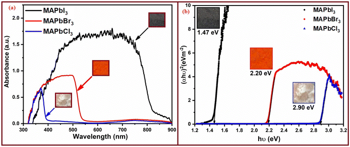 | ||
| Fig. 3 (a) The UV-visible absorption spectra of the three perovskite powders and (b) their corresponding optical bandgap values. | ||
These optical bandgap values are crucial for understanding the energy levels and electronic properties of perovskite materials, with significant implications for their potential applications in optoelectronic devices, such as solar cells and light-emitting devices. In our study, we observed that MAPbI3 with the optical band gap value of 1.47 eV represents the optimal perovskite material for solar photoelectric energy conversion devices, compared to the other materials analyzed, which had band gaps of 2.20 eV and 2.90 eV, respectively, calculated from their absorption spectra. These values are higher than the band gaps observed in the case of Cr-doped CIGS, which had values of around 1.15–1.20 eV.51 Conversely, our obtained values precisely adhere to the patterns established in the existing literature, confirming that our determined energy band gap falls within the perovskite range.47
3.4. Analysis of the conductivity
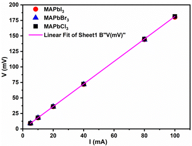
Knowing the sheet sample thickness (t), the in-plane apparent resistivity (ρs) of the perovskites, commonly named the sheet resistivity, was obtained from eqn (2), and the sheet conductivity was calculated from the inverse of the sheet resistivity, as indicated in eqn (3). The results obtained are given in Table 1.
On the other hand, from both Fig. 4 and Table 2, we can observe that the perovskites exhibit quite similar sheet resistance as the slopes of the straight lines for the three samples are practically the same. The values of the sheet resistivity obtained for the perovskites expressed in terms of the International Annealed Copper Standard (%IACS) are about 0.1% IACS. The values of in-plane conductivity (σs) of all perovskites are 489 × 103 S m−1, 486 × 103 S m−1 and 510 × 103 S m−1 for MAPbBr3, MAPbCl3 and MAPbI3, respectively. Considering that 100% IACS is defined as the conductivity corresponding to a volume resistivity of 17.241 nΩ m at 20 °C, these values are around 86 times lower than that obtained for the TiB2p/Cu composite powder prepared by the in situ reaction in combination with rolling, which were measured using a Sigma 2008B eddy current conductivity instrument.52
| Samples | Thickness (nm) | Sheet resistivity (ρs) (nΩ m) | Sheet resistance (Rs) (Ω) | Sheet conductivity (σs) × 10−3 (S m−1) |
|---|---|---|---|---|
| MAPbBr3 | 251 ± 12 | 2046 ± 18 | 8.15 ± 0.02 | 489 ± 4 |
| MAPbCl3 | 255 ± 14 | 2058 ± 16 | 8.07 ± 0.02 | 486 ± 4 |
| MAPbI3 | 240 ± 10 | 1961 ± 15 | 8.17 ± 0.02 | 510 ± 3 |
Focused Ion Beam (FIB) was employed to ascertain the cross-sectional profile of the thin films, which is consistent with the literature, measuring approximately 250 nm. All three samples have almost the same thickness because we are using the same parameters for deposition through the spin coating technique. Furthermore, our results match the existing literature.53
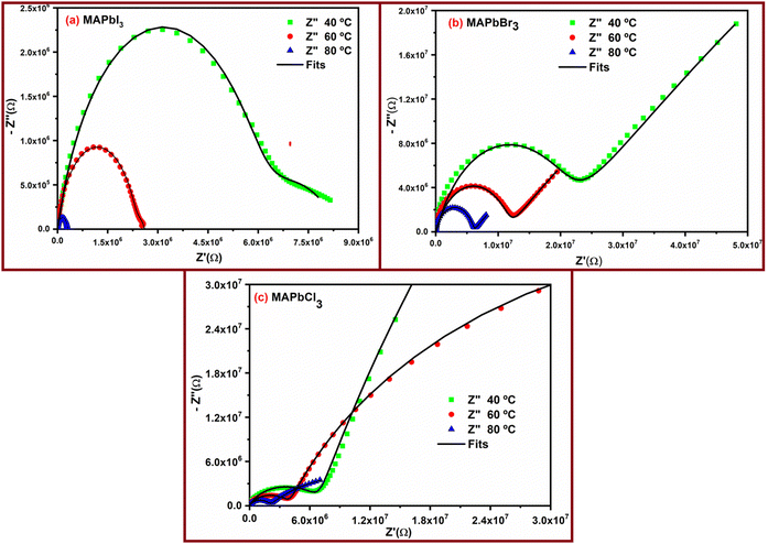 | ||
| Fig. 5 Nyquist plots representing the complex impedance vs. real part of the impedance, at various temperatures (40 °C, 60 °C and 80 °C) for the MAPbI3 sample (a), MAPbBr3 sample (b) and MAPbCl3 sample (c), respectively. The solid lines represent the fits of eqn (5) to the experimental data. Nyquist plots for the other temperatures are given in Fig. SI2, SI3 and SI4 of ESI.† | ||
The modelling of experimental data represented in the Nyquist plot shown in Fig. 5 was obtained from the equivalent circuit shown in ESI† (Fig. SI1). This equivalent circuit is formed by a parallel combination of a resistance R1 and a constant phase element (CPE1), the sub-circuit (R1-CPE1), in series with a parallel resistance (R2) with a constant phase element (CPE2), the sub-circuit (R2-CPE2), where the impedance of the CPE is identified from the expression.
 | (4) |
 | (5) |
In Table 3 we can see the parameters R, R1, R2, Q1, Q2, α1, and α2, determined using the equivalent circuit fitted following expression (5). Considering that the relation between complex impedance and complex conductivity is given by,
 | (6) |
 | (7) |
 where yi is the measured data set, ŷi is the modelled data set, ȳ is the mean of the measured data, σr2 is the residual variance and σy2 is the variance54
| Samples | T (°C) | R 1 (Ω) | Q 1 | α 1 | R 2 (Ω) | Q 2 | α 2 | r 2 | σ (S cm−1) |
|---|---|---|---|---|---|---|---|---|---|
| MAPbI3 | 20 | 6.0 × 10⁷ | 9.5 × 10⁻¹⁰ | 0.77 | 4.1 × 10⁷ | 7.5 × 10⁻⁹ | 0.35 | 0.900 | 3.7 × 10⁻⁹ |
| 40 | 5.9 × 10⁶ | 4.3 × 10⁻¹⁰ | 0.81 | 2.6 × 10⁶ | 17 × 10−8 | 0.45 | 0.996 | 4.4 × 10⁻⁸ | |
| 60 | 2.4 × 10⁶ | 1.6 × 10⁻¹⁰ | 0.85 | 2.5 × 10⁵ | 13 × 10−8 | 0.70 | 0.983 | 1.4 × 10⁻⁷ | |
| 80 | 3.0 × 10⁵ | 7.7 × 10⁻¹¹ | 0.92 | 3.0 × 10³ | 8 × 10⁻⁶ | 0.80 | 0.993 | 1.2 × 10⁻⁶ | |
| 100 | 1.9 × 10⁴ | 5.0 × 10⁻¹¹ | 0.98 | 3.0 × 10² | 1.8 × 10⁻² | 0.01 | 0.997 | 1.9 × 10⁻⁵ | |
| 120 | 2.1 × 10³ | 7.2 × 10⁻¹¹ | 0.96 | 2.0 × 10² | 1.0 × 10⁻² | 0.10 | 0.998 | 1.6 × 10⁻⁴ | |
| 140 | 4.5 × 10² | 1.1 × 10⁻⁹ | 0.83 | 2.0 × 10² | 1.5 × 10⁻² | 0.18 | 0.990 | 5.7 × 10⁻⁴ | |
| 160 | 1.7 × 10² | 2.0 × 10⁻⁹ | 0.80 | 1.2 × 10² | 4.0 × 10⁻² | 0.20 | 0.550 | 1.3 × 10⁻³ | |
| 180 | 8.7 × 101 | 3.0 × 10⁻⁹ | 0.80 | 2.5 × 101 | 9.0 × 10⁻² | 0.24 | 0.507 | 3.3 × 10⁻³ | |
| 200 | 4.3 × 101 | 5.0 × 10⁻⁹ | 0.80 | 2.0 × 100 | 2.0 × 10⁻¹ | 0.30 | 0.862 | 8.2 × 10⁻³ | |
| MAPbBr3 | 20 | 4.0 × 10⁷ | 1.8 × 10⁻¹⁰ | 0.78 | 5.3 × 10⁸ | 8.8 × 10⁻⁹ | 0.71 | 1.000 | 1.7 × 10⁻⁹ |
| 40 | 2.0 × 10⁶ | 1.7 × 10⁻¹⁰ | 0.78 | 3.5 × 10⁸ | 3.3 × 10⁻⁸ | 0.41 | 0.994 | 1.7 × 10⁻⁹ | |
| 60 | 1.2 × 10⁷ | 1.5 × 10⁻¹⁰ | 0.77 | 1.0 × 10⁸ | 1.2 × 10⁻⁷ | 0.42 | 0.986 | 8.2 × 10⁻⁹ | |
| 80 | 6.1 × 10⁶ | 1.3 × 10⁻¹⁰ | 0.80 | 2.1 × 10⁷ | 4.3 × 10⁻⁷ | 0.45 | 0.989 | 4.5 × 10⁻⁸ | |
| 100 | 2.9 × 10⁶ | 1.1 × 10⁻¹⁰ | 0.83 | 1.0 × 10⁷ | 4.0 × 10⁻⁶ | 0.35 | 0.990 | 4.7 × 10⁻⁷ | |
| 120 | 1.4 × 10⁵ | 1.0 × 10⁻¹⁰ | 0.88 | 1.0 × 10⁶ | 2.0 × 10⁻⁵ | 0.30 | 0.999 | 1.3 × 10⁻⁶ | |
| 140 | 6.5 × 10⁵ | 7.0 × 10⁻¹¹ | 0.91 | 2.1 × 10⁵ | 6.0 × 10⁻⁵ | 0.27 | 1.000 | 3.1 × 10⁻⁶ | |
| 160 | 3.1 × 10⁵ | 4.8 × 10⁻¹¹ | 0.95 | 6.0 × 10⁴ | 3.0 × 10⁻⁴ | 0.25 | 1.000 | 5.5 × 10⁻⁶ | |
| 180 | 1.4 × 10⁵ | 2.3 × 10⁻¹¹ | 0.95 | 1.0 × 10⁴ | 2.0 × 10⁻³ | 0.20 | 0.899 | 1.4 × 10⁻⁵ | |
| 200 | 3.6 × 10⁴ | 1.2 × 10⁻¹⁰ | 0.91 | 1.0 × 10³ | 1.0 × 10⁻² | 0.22 | 0.993 | 3.8 × 10⁻⁵ | |
| MAPbCl3 | 20 | 8.7 × 10⁶ | 3.1 × 10⁻¹⁰ | 0.81 | 5.1 × 10⁸ | 1.1 × 10⁻⁸ | 0.80 | 0.999 | 1.4 × 10⁻¹⁰ |
| 40 | 6.8 × 10⁶ | 3.7 × 10⁻¹⁰ | 0.79 | 5.1 × 10⁸ | 1.2 × 10⁻⁸ | 0.85 | 1.000 | 1.4 × 10⁻¹⁰ | |
| 60 | 3.9 × 10⁶ | 5.0 × 10⁻¹⁰ | 0.78 | 1.0 × 10⁸ | 2.6 × 10⁻⁸ | 0.79 | 0.989 | 6.9 × 10⁻¹⁰ | |
| 80 | 2.0 × 10⁶ | 5.0 × 10⁻¹⁰ | 0.81 | 1.7 × 10⁷ | 15 × 10−8 | 0.56 | 0.908 | 3.8 × 10⁻⁹ | |
| 100 | 1.0 × 10⁶ | 6.0 × 10⁻¹⁰ | 0.76 | 8.0 × 10⁵ | 23 × 10−7 | 0.52 | 0.999 | 3.9 × 10⁻⁸ | |
| 120 | 4.4 × 10⁵ | 3.1 × 10⁻¹⁰ | 0.83 | 2.0 × 10⁵ | 15 × 10−6 | 0.49 | 0.999 | 1.1 × 10⁻⁷ | |
| 140 | 2.0 × 10⁵ | 2.0 × 10⁻¹⁰ | 0.87 | 8.0 × 10⁴ | 33 × 10−6 | 0.51 | 1.000 | 2.6 × 10⁻⁷ | |
| 160 | 7.6 × 10⁴ | 2.0 × 10⁻¹⁰ | 0.91 | 8.0 × 10⁴ | 15 × 10−5 | 0.46 | 0.982 | 4.6 × 10⁻⁷ | |
| 180 | 3.2 × 10⁴ | 2.1 × 10⁻¹⁰ | 0.91 | 2.8 × 10⁴ | 16 × 10−5 | 0.58 | 0.979 | 1.2 × 10⁻⁶ | |
| 200 | 1.2 × 10⁴ | 1.1 × 10⁻¹⁰ | 0.94 | 1.0 × 10⁴ | 27 × 10−5 | 0.67 | 0.998 | 3.2 × 10⁻⁶ |
In our study, the powder sample thickness was measured using a micrometer, with values being 561 ± 17 μm, 672 ± 20 μm, and 291 ± 10 μm for MAPbBr3, MAPbCl3 and MAPbI3, respectively, and the area of the sample sandwiched between the two electrodes is A = 0.785 cm2, and we can determine the values of the conductivity at each temperature by the determination of the real part of the impedance, Z′(ω,T).
Conductivity values obtained for the powders MAPbI3, MAPbBr3 and MAPbCl3 following the Cole–Cole plots shown in Fig. 5 are given in the last column in Table 1. For this, we have considered the equivalent circuit displayed in Fig. SI1 (ESI†) and eqn (5) to simulate the experimental results and obtain the parameters R, R1 and R2, given in Table 3. Notice that the value of R determined in all the fits was zero (R = 0). From the values obtained for the resistances, the values of conductivity were calculated using eqn (7), where Z′(ω,T) is equal to (R1 + R2). In the last column of Table 3 we have gathered the values of the conductivities obtained for the samples MAPbI3, MAPbBr3 and MAPbCl3, respectively.
A close inspection of Fig. 5 shows the existence of a different behavior of the sample MAPbI3 than MAPbBr3 and MAPbCl3, respectively. This can be due to the grain boundary polarization as a highly capacitive phenomenon, which is characterized by larger relaxation times than the polarization mechanism in the bulk where the behavior of the grains is similar to that of a semiconductive material, and such a phenomenon is more apparent in the sample MAPbI3 than in MAPbBr3 and MAPbCl3, respectively. This fact usually results in the appearance of two separate arcs in the Z′′ versus Z′ plots, one representing the bulk effect at high frequencies, while the other representing the surface effect in the lower frequency range. The complex impedance spectrum was interpreted for all the samples by means of the equivalent circuit shown in Fig. SI1 (ESI†). There are cases where the experimental data exhibit a spike at low frequencies, typically occurring at lower temperatures of around 20 and 40 °C. As observed, all the spectra demonstrate a prominent arc wherein a segment of the semicircle intercepts at the origin of coordinates at higher frequencies (R = 0), while the other segment either intercepts or tends to approach intercepting as Z′′ approaches zero, giving R1 and R2 at each temperature. Utilizing these values, we have calculated the perovskite conductivity. This is achieved by considering the effective area of the sample, which is equivalent to the area of the sample situated between the two electrodes (S = 0.785 cm2), along with its thickness (L). In our study, the powder sample thicknesses measured using a micrometer were 561 ± 17 μm, 672 ± 20 μm, and 291 ± 10 μm for MAPbCl3, MAPbBr3, and MAPbI3, respectively.
The outcomes derived from the Nyquist plot, which were employed to ascertain the sample's resistance, were further subjected to eqn (7) to determine the direct current conductivity (σdc) at specific temperatures. These calculated values are listed in the column specified by σ (S cm−1) in Table 3. It is crucial to note that this approach is considered an indirect method because the determined resistance is contingent on the criteria of the chosen equivalent circuit.
From Table 3 we can see that in the entire range of temperatures studied, the conductivity values follow the trend σMAPbCl3 < σMAPbBr3 < σMAPbI3. These values vary between 10−9 and 10−3 S cm−1 for MAPbI3, between 10−10 and 10−6 S cm−1 for MAPbCl3, and between 10−9 and 10−5 S cm−1 in the case of MAPbBr3. These values were determined between 20 and 200 °C, respectively. All these values were similar to or even higher than the values reported by Leupold et al.55 in the study carried out on the electrical conductivity as a function of the iodine partial pressure of powder aerosol deposited MAPBI3 calculated from impedance spectra, as is done in this study.
The differences observed in conductivity, based on the type of dopant, can be attributed to variations in the concentration of mobile charges. Furthermore, their mobility is influenced by the strength of interactions with different stages of perovskites at various temperatures. A thorough investigation of this aspect will be conducted beforehand.
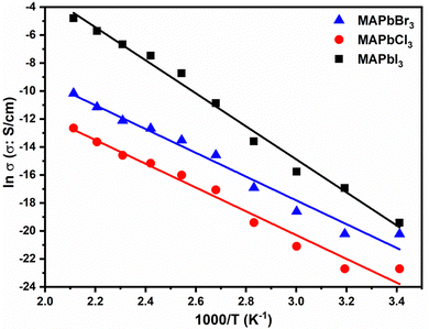
In Fig. 6 are plotted the conductivity values tabulated in Table 3 obtained for the different perovskites in the entire range of temperatures studied.
Fig. 6 distinctly illustrates the relationship between conductivity and temperature. A close inspection of Fig. 6 shows that the temperature dependence of the conductivity of perovskites exhibits an Arrhenius behavior in the entire range of temperatures studied. Such behavior has been necessary to understand the dynamics process of the different agents of perovskites. However, a little change can be observed around 100 °C in the conductivity patterns of all samples indicating that the perovskites exhibit significant similarities, being more prominent for MAPbBr3 and MAPbCl3. In both cases an increase in conductivity as temperature rises is evident.
From Fig. 6 we have calculated the activation energy associated with the conductivity. For this we have fitted the experimental results of the conductivities obtained from the Nyquist plot shown in Fig. 5 for all perovskites. The values of the activation energy follow the trend Eact (MAPbBr3) = (70.7 ± 4.0) kJ mol−1 (i.e., 0.73 ± 0.04 eV) < Eact (MAPbCl3) = (71.5 ± 4.0) kJ mol−1 (i.e., 0.74 ± 0.04 eV) < Eact (MAPbI3) = (98.1 ± 3.6) kJ mol−1 (i.e., 1.02 ± 0.04 eV).
It is noteworthy that the conductivity of the MAPbBr3 sample is slightly higher than that of the MAPbCl3 sample. However, upon analyzing the MAPbI3 sample a remarkably mild alteration in conductivity becomes evident at temperatures between 80 °C and 100 °C. This sudden change might be attributed to the structural modifications that occur as the temperature surpasses these values, which might be due to a change in wettability and a change in the crystallinity and size of crystal grains. It is likely that the properties of the material undergo significant shifts due to these temperature thresholds. Notice that these sudden changes in behavior have also been observed at temperatures higher than 100 °C from XRD for MAPbI3, indicating that PbI2 is not fully converted to perovskite and an increase in the temperature results in the degradation of the MAPbI3 phase.56
Considering the nature of these materials, it is noteworthy that at temperatures exceeding 80–100 °C, distinct relaxation or orientation processes can be induced in both the inorganic and organic ions present within the samples. It is intriguing to observe that these processes tend to manifest more gradually in the case of MAPbI3, as opposed to perovskites with Cl or Br. This phenomenon aligns with findings described by various researchers,57–59 who suggest a connection between these behaviors and the reorientation angle of MA+ ions. These observations could be attributed to the constraints imposed by the stacking of the PbI64 octahedral framework in a TP (tetrahedral) arrangement. This arrangement might impact the intramolecular or axial rotation of organic cations along with intricate hydrogen bonding interactions with inorganic cages. These factors could collectively contribute to the observed variations in relaxation and orientation processes within the distinct types of perovskite materials.57–61
In MAPbI3, the presence of iodide vacancies allows for the migration of iodide, and thus iodide vacancies also migrate.11,12 The latter are formed, for example, when an iodide ion at a regular lattice site moves to an interstitial site, leaving an iodide vacancy at the original iodide lattice site (referred to as the (anion) Frenkel defect).13 Alternatively. the formation of Schottky defects, which results in the formation of MA vacancies and iodide vacancies, is well possible in MAPbI3 and results in the formation of iodide vacancies,12,14 Iodide interstitials, iodide or MA vacancies, all represent classical point defects that can widely determine the electrical transport behavior of halide perovskites.5 Accordingly, defect chemical modeling combined with appropriate characterization methods offers a powerful way to gain in-depth understanding of the electrical conductivity in halide perovskites.13,15,16
From Fig. 6 we have calculated the activation energy associated with the conductivity. For this we have fitted the experimental results of the conductivities obtained from the Nyquist plot shown in Fig. 5 for all perovskites. The values of the activation energy follow the trend Eact (MAPbBr3) = (70.7 ± 4.0) kJ mol−1 (i.e., 0.73 ± 0.04 eV) < Eact (MAPbCl3) = (71.5 ± 4.0) kJ mol−1 (i.e., 0.74 ± 0.04 eV) < Eact (MAPbI3) = (98.1 ± 3.6) kJ mol−1 (i.e., 1.02 ± 0.04 eV).
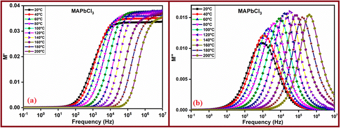
Fig. 7 presents the frequency dependencies of the real and imaginary parts of the complex modulus for the sample MAPbCl3. The corresponding behaviors for the other perovskites, MAPbI3 and MAPbBr3, can be found in the ESI† (Fig. SI5 and SI6). Examining Fig. 7, we can observe that the variations of the real part of the complex modulus (M′) tend to converge towards zero at lower frequencies, while at higher frequencies, they tend towards 1/εr.∞, where εr.∞ denotes the electrical permittivity of the perovskite. The values determined in our study were 30 ± 2, 29 ± 2 and 31 ± 1 for MAPbCl3, MAPbBr3 and MAPbI3, respectively. These values are quite similar to the value 30, considered by Prochowicz et al.62 to calculate the defect density in the perovskite MAPbI3.
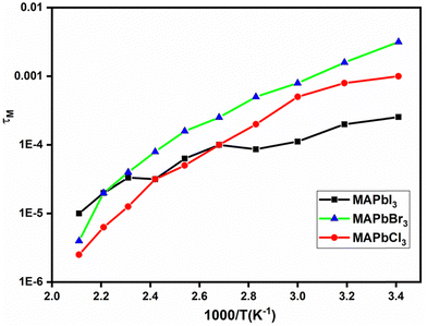
In contrast, the complex modulus M′′ displays frequency-dependent changes, characterized by a symmetrical peak with varying width that decreases with rising temperature in the case of the MAPbCl3 sample. This symmetry is also present for the MAPbBr3 sample. However, for the MAPbI3 sample, the behavior is notably asymmetric, with two peaks observed at lower temperatures. This asymmetry might be attributed to the sample's tendency to retain moisture, influencing the mobility of two distinct ions, I− and H+. The frequency at the point of maximum is intricately connected to the relaxation time (τM). This reciprocal relationship can be elucidated by considering the values derived for ωM = 2πfM from the peaks identified for M′′. Notably, these values correspond to the relaxation time and, by extension, will be contingent on the prevailing temperature conditions.
As depicted in Fig. 8, the relationship between relaxation time and temperature is non-linear. On one hand, both MAPbCl3 and MAPbBr3 samples demonstrate a similar trend across the entire temperature range, featuring two distinct thermally activated processes. On the other hand, the MAPbI3 sample exhibits two distinct behaviors: one below 120 °C and another above this temperature. This behavior presents variations that could potentially be linked to the effects of degradation leading to abrupt structural changes or could be related to changes in iodine vacancies and holes between low and high temperatures, as observed for the total conductivity of the MAPbI3 perovskite as a function of the iodine partial pressure.55 These structural changes are likely to involve intramolecular or axial rotations of organic cations, coupled with subtle hydrogen bond interactions with inorganic cages. Such changes are particularly relevant in the context of our perovskites containing I−, Cl−, and Br− ions.58–62 Remarkably, these behaviors stand in contrast to the alterations observed in conductivity. This can be attributed to the consistent value of the real part of permittivity at frequencies approaching infinity, as demonstrated in Fig. 7. It is important to consider that τ = εr.∞/σ, reinforcing the reciprocal relationship between relaxation time and conductivity alterations.
![[thin space (1/6-em)]](https://www.rsc.org/images/entities/char_2009.gif) δ) of a sample, a distinct peak is observed. This is notably evident in the Nyquist plot, where a semicircle emerges, and the point of intersection between the real and imaginary parts of impedance, where the imaginary part is zero, determines the sample's resistance. This behavior can be attributed to the fact that the impedance spectrum of perovskites is essentially dictated by the movement of a single type of ion, resulting in the observation of a sole relaxation time. By identifying the maxima in tan
δ) of a sample, a distinct peak is observed. This is notably evident in the Nyquist plot, where a semicircle emerges, and the point of intersection between the real and imaginary parts of impedance, where the imaginary part is zero, determines the sample's resistance. This behavior can be attributed to the fact that the impedance spectrum of perovskites is essentially dictated by the movement of a single type of ion, resulting in the observation of a sole relaxation time. By identifying the maxima in tan![[thin space (1/6-em)]](https://www.rsc.org/images/entities/char_2009.gif) δ values, it is possible to estimate the diffusion coefficient of the charges in the perovskites25,59,63
δ values, it is possible to estimate the diffusion coefficient of the charges in the perovskites25,59,63
 | (8) |
 | (9) |
Fig. 9 presents the experimental tan![[thin space (1/6-em)]](https://www.rsc.org/images/entities/char_2009.gif) δ values for the perovskites across all temperatures. Moreover, a noteworthy observation can be rationalized: the displacement of the loss tangent peaks towards the higher frequency side is closely linked to the activation of anions I−, Cl−, and Br−. On the other hand, the value of the loss tangent of the peak is higher in the case of MAPbBr3 and MAPbCl3 than that in the case of MAPbI3, and a change in this intensity is clearly observed between low and high temperatures for all the perovskites. This behavior mirrors the findings observed for electrolytes incorporating ionic liquids.64–67 Based on the peaks observed in these figures, we have extracted the values of ωtan
δ values for the perovskites across all temperatures. Moreover, a noteworthy observation can be rationalized: the displacement of the loss tangent peaks towards the higher frequency side is closely linked to the activation of anions I−, Cl−, and Br−. On the other hand, the value of the loss tangent of the peak is higher in the case of MAPbBr3 and MAPbCl3 than that in the case of MAPbI3, and a change in this intensity is clearly observed between low and high temperatures for all the perovskites. This behavior mirrors the findings observed for electrolytes incorporating ionic liquids.64–67 Based on the peaks observed in these figures, we have extracted the values of ωtan![[thin space (1/6-em)]](https://www.rsc.org/images/entities/char_2009.gif) δmax and (tan3δ)max.ω. With knowledge of the samples' thickness, we calculated the diffusion coefficients of the perovskites, and utilizing eqn (8), we then computed the corresponding mobilities. This series of calculations provides valuable insights into the mobility of charged particles within these materials under specific conditions.
δmax and (tan3δ)max.ω. With knowledge of the samples' thickness, we calculated the diffusion coefficients of the perovskites, and utilizing eqn (8), we then computed the corresponding mobilities. This series of calculations provides valuable insights into the mobility of charged particles within these materials under specific conditions.
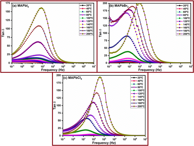 | ||
Fig. 9 The variation of loss tan![[thin space (1/6-em)]](https://www.rsc.org/images/entities/char_2009.gif) δ with frequency for perovskites: (a) MApbI3, (b) MAPbBr3, and (c) MAPbCl3, in the entire range of temperatures studied. δ with frequency for perovskites: (a) MApbI3, (b) MAPbBr3, and (c) MAPbCl3, in the entire range of temperatures studied. | ||
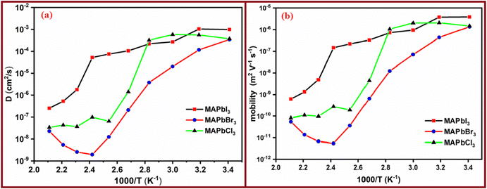
Fig. 10 illustrates the temperature-dependent diffusion and mobility coefficients of the perovskites. From Fig. 10A, it becomes apparent that the diffusion coefficient values decline as the temperature rises. This behavior stands in stark contrast to what is typically observed in ionic diffusion through polymer electrolytes.34,65,66 Upon a thorough examination of this figure, a remarkable trend emerges: the diffusion coefficients exhibit impressive performance at lower temperatures, subsequently declining by approximately three orders of magnitude when comparing the diffusivity at 40 °C to that at 120 °C. On a contrasting note, across the entire temperature range, two distinct variations become evident, similar to the variations observed in the temperature-dependent behavior of conductivity. This behavior is expected and can be attributed to the similar patterns exhibited by the mobilities of perovskites.
On the other hand, a close inspection of Fig. 10b shows that the mobilities of perovskites follow the trend μ(MAPbI3) > μ(MAPbCl3) > μ(MAPbBr3). In the case of the MAPbI3 perovskite we have found that mobility varies between 6 × 10⁻¹⁰ m2 V−1 s−1 and 4 × 10⁻⁶ m2 V−1 s−1, depending on temperature. These values for MAPbBr3 and MAPbCl3 are slightly lower than the corresponding electronic mobilities found in the literature (4 × 10⁻⁵–35 × 10−4 m2 V−1 s−1).67 However, in the case of MAPbI3 they are quite similar. For example, at 80 °C the value found in this work was 7 × 10⁻⁷ m2 V−1 s−1 (i.e., 7 × 10⁻³ cm2 V−1 s−1 found by Stranks et al.68). On the other hand, our values for all perovskites are higher than the values given by ref. 55 and 68, where the values found at 70 °C for MAPbI3 were significantly lower (μVi* ≅ 5 × 10⁻⁸ cm2 V−1 s−1 and μMA ≅ 8 × 10⁻¹¹ cm2 V−1 s−1), respectively.
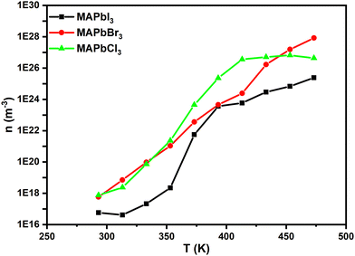
In general, in polyelectrolytes and semiconductors considered as binary systems, the total electrical conductivity is the sum of the contributions of all the constituent charge carriers, i.e., σ = σ+ + σ−. In the case of perovskites MAPbX3 (X = Cl, Br, I) the highest possible contribution to the ionic conductivity is from the anions. Therefore, the anion conductivity can be estimated supposing that the anion transference number is practically equal to one. In this approximation, the cations are practically immobile due to the reduced mobility because their size in comparison with the other counterpart is higher. Therefore, the cation mobility is negligible and thus the dominated mobility will be mainly restricted to the anion contribution (i.e., X− = Cl−, Br− and I−, respectively). In these cases, the ionic conductivity can be described as σ− = σ. If charge carriers do not interact with each other, we can estimate the charge carrier density, (n), from the Nernst–Einstein relationship and eqn (9) as
 | (10) |
From Fig. 11 we can see that in the perovskites the charge carrier's density, n (m−3), increases with the temperature increase, with its value being around 1017 m−3 at 20 °C and 1027 m−3 at 180 °C for the perovskites MAPbCl3 and MAPbBr3. For both perovskites, in the entire range of temperatures studied the charge carrier's density is the highest compared to that of MAPBI3. This is due to the fact that the relation σ/D is lower for MAPbI3 than that for the others. On the other hand, a change of behavior at 100 °C seems to be observed. Finally, these values agree with the range of literature-based values calculated, as observed for MAPbI3.69
Lastly, to understand the interface effects between MAPbI3 and reference MAPbCl3, we have calculated the Debye length based on the peaks of loss tangent (tan![[thin space (1/6-em)]](https://www.rsc.org/images/entities/char_2009.gif) δ) following ref. 23, 25, 34 and 63. It is important to note that there is an error in eqn (23) of ref. 63. The accurate expression should be:
δ) following ref. 23, 25, 34 and 63. It is important to note that there is an error in eqn (23) of ref. 63. The accurate expression should be:
 | (11) |
 . It is interesting to note that the determination of the Debye length, defined as
  , where kB is the Boltzmann constant, T the temperature, ε0 the vacuum permittivity, ε∝ the static permittivity, q the charge quantity of the ion and n the ionic charge density imbibed into the perovskites, has been carried out without the need to know the values of ε∝ and the density of the charge carriers (n), which must be determined by means of knowledge of mobility (μ) or diffusivity (D). This avoids the possible errors that the models provide in the determination of these parameters. In our case, we have opted for its determination based on the experimental results of the loss tangent for each of the perovskites where the curves of loss tangent display peaks corresponding to the maxima in tan
![[thin space (1/6-em)]](https://www.rsc.org/images/entities/char_2009.gif) δ, which are associated with the conductivity. In this way, the value of LD is calculated from the experimental results obtained for tan
δ, which are associated with the conductivity. In this way, the value of LD is calculated from the experimental results obtained for tan![[thin space (1/6-em)]](https://www.rsc.org/images/entities/char_2009.gif) δ from EIS and therefore we think that it will have less error than if it had been determined from the values of the parameters such as n, D, τ, or μ, where models are necessary for its determination.
δ from EIS and therefore we think that it will have less error than if it had been determined from the values of the parameters such as n, D, τ, or μ, where models are necessary for its determination.
By utilizing eqn (11) and leveraging the experimental values acquired for tan![[thin space (1/6-em)]](https://www.rsc.org/images/entities/char_2009.gif) δmax for the various perovskites, we derived the Debye length values. These results have been graphed in Fig. 12, providing a visual representation of the Debye lengths corresponding to the different perovskites.
δmax for the various perovskites, we derived the Debye length values. These results have been graphed in Fig. 12, providing a visual representation of the Debye lengths corresponding to the different perovskites.
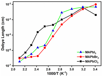 | ||
| Fig. 12 The values of the Debye length that were computed using eqn (11) for the perovskites examined across the entire range of temperatures studied. | ||
As shown in Fig. 12, the calculated results for the Debye length, obtained from the peaks of the loss tangent using eqn (11), exhibit a similar behavior for the perovskites MAPbCl3 and MAPbBr3 throughout the entire range of temperatures studied. In contrast, the perovskite MAPbI3 displays an abnormal behavior, with a drastic decrease in the thickness of the Debye layer observed from 50 °C onwards. These distinct behaviors may be related to the long or short-range hopping distances that the anions have to overcome to move and transfer electrons to the conduction band. The difference in the behavior of MAPbI3 could indicate the unique charge transport characteristics of this particular perovskite, which may be influenced by the type of anions and their mobility at different temperatures. Our results for MAPbI3 were LD ≅ 2 × 10⁻⁶ m, at 20 °C, agreeing with the values observed by Samuel D. Stranks et al.71 where Debye lengths of 120 nm and 105 nm for electron and holes were obtained in the case of MAPbI3. Further investigation is needed to fully understand the underlying mechanisms behind these observed trends.
4. Conclusions
Various perovskite powders of MAPbX3 were synthesized, where X represents iodine (I), bromine (Br), or chlorine (Cl). The main objective of this research was to investigate the influence of different halides on the photovoltaic performance of perovskites. To achieve this, several characterization methods were conducted to understand the properties of the perovskite powders MAPbX3 (X = I, Br, Cl) with a specific focus on determining their optical and conductivity properties. The corresponding X-ray diffraction (XRD) spectrum of each perovskite powder sample is also shown in Fig. 1. The XRD spectra displayed characteristic peaks that aligned well with those reported in the literature. This indicates that the prepared perovskite powders have a well-defined crystalline structure consistent with the known properties of MAPbX3 compounds. Overall, the HRTEM analysis provided valuable insights into the nanostructure, crystal quality, and crystallographic information of the MAPbX3 perovskite powders. These findings are essential for a comprehensive understanding of the properties and potential applications of these perovskite materials. This study contributes to the advancement of knowledge in the field of perovskite materials and their use in various applications.The UV-visible spectra of perovskite powders (MAPbCl3, MAPbBr3, and MAPbI3) were analyzed, revealing distinct absorption onsets for each composition, with MAPbCl3 absorbing light in the ultraviolet and visible regions at 427 nm, MAPbBr3 absorbing at 563 nm in the visible spectrum, and MAPbI3 absorbing at 843 nm in the near-infrared region. The corresponding optical bandgap values are 2.90 eV, 2.20 eV, and 1.47 eV, respectively.
The analysis of electrochemical impedance spectroscopy reveals that perovskite materials with iodine (I), chlorine (Cl), and bromine (Br) exhibit optimal conductivities, making them suitable semiconductor materials. As the temperature increases, their conductivities also increase, following the trend σdc (MAPbI3) < σdc (MAPbCl3) < σdc (MAPbBr3). Furthermore, the conductivity activation energies of these materials vary with temperature. The values of the activation energy follow the trend Eact (MAPbBr3) = (70.7 ± 4.0) kJ mol−1 (i.e., 0.73 ± 0.04 eV) < Eact (MAPbCl3) = (71.5 ± 4.0) kJ mol−1 (i.e., 0.74 ± 0.04 eV) < Eact (MAPbI3) = (98.1 ± 3.6) kJ mol−1 (i.e., 1.02 ± 0.04 eV).
Electrochemical impedance spectroscopy (EIS) studies revealed a significant change in the conductivity of the MAPbI3 perovskite at temperatures between 80 °C and 120 °C. This change could be attributed to structural modifications induced when the temperature exceeds these values. The through-plane conductivity increases around 103 times when the temperature increases from 60 °C to 120 °C and around 100 times from 120 °C to 200 °C. Meanwhile, the sheet conductivity (in-plane conductivity) measured at ambient temperature reveals that sheet resistivity obtained for the perovskites expressed in terms of the International Annealed Copper Standard (% IACS) is about 0.1% IACS, a value equivalent to 1000 times lower than annealed copper. The sheet conductivities were 489 × 103 S m−1, 486 × 103 S m−1 and 510 × 103 S m−1 for MAPbBr3, MAPbCl3 and MAPbI3, respectively.
At low temperatures, the diffusivities of the perovskite materials exhibit a significant decrease of approximately three orders of magnitude when comparing the diffusivity values at 40 °C to those at 120 °C. Moreover, throughout the entire range of temperatures studied, two distinct variations in diffusivity are observed, which resemble the behavior observed in the variation of conductivity with temperature. Similarly, perovskite mobility also displays a similar behavior. In the case of the MAPbI3 perovskite we have found that mobility varies between 6 × 10⁻¹⁰ m2 V−1 s−1 and 4 × 10⁻⁶ m2 V−1 s−1, depending on temperature. These values for MAPbBr3 and MAPbCl3 are slightly lower than the corresponding electronic mobility found in the literature (4 × 10⁻⁵–35 × 10−4 m2 V−1 s−1). The variation of relaxation time with temperature is not linear. The samples MAPbCl3 and MAPbBr3 show a similar tendency over the entire temperature range studied, with two different thermally activated processes. However, the sample MAPbI3 exhibits two distinct behaviors, one below 120 °C and the other above this temperature, with a variation that could potentially be associated with possible degradation effects leading to sudden structural changes.
This study provides valuable insights for optimizing the performance of perovskite solar cells. Understanding how dopants influence the electrical conductivity and photovoltaic properties of the perovskite materials, this work will enable researchers to design and engineer more efficient and stable solar cell devices based on MAPbX3 perovskites. These findings indicate that the conductivity of the perovskite materials is temperature-dependent, and the variations can significantly impact their performance as semiconductor materials at different temperatures.
Author contributions
Shafi Ullah: conceptualization, investigation, methodology, writing – original draft; Andreu Andrio: investigation, supervision, validation; Julia Marí-Guaita: conceptualization, investigation, methodology, writing – original draft; Hanif Ullah: investigation, methodology; writing – original draft; Antonio Méndez-Blas: visualization, reviewing, visualization, reviewing and editing; Bernabe Mari: visualization, supervision, validation; Roxana M. del Castillo Vázquez: visualization, reviewing, visualization, reviewing and editing; and Vicente Compañ: conceptualization, investigation, methodology, writing – original draft, visualization supervision, validation, reviewing, and editing.Conflicts of interest
The authors declare that they have no known competing financial interests or personal relationships that could have appeared to influence the work reported in this paper.Acknowledgements
The author Shafi Ullah acknowledges the post-doctoral contract supported by the RRHH (Human Resources for Research) program, postdoctoral contract (PAID-10-20) Universitat Politècnica de Valencia (UPV), and Ministerio de Economía y Competitividad under Grant Number PID 2019–107137 RB-C21. Antonio Mendez-Blas acknowledges CONACYT, Mexico (Sabbatical Grant 2022) and VIEP-BUAP.References
- J. Burschka, N. Pellet, S. J. Moon, R. Humphry-Baker, P. Gao, M. K. Nazeeruddin and M. Grätzel, Sequential deposition as a route to high-performance perovskite-sensitized solar cells, Nature, 2013, 499(7458), 316–319 CrossRef CAS PubMed
.
- H. S. Kim, C. R. Lee, J. H. Im, K. B. Lee, T. Moehl, A. Marchioro and S. J. Moon, et al., Lead iodide perovskite sensitized all-solid-state submicron thin film mesoscopic solar cell with efficiency exceeding 9%, Sci. Rep., 2012, 2(1), 591 CrossRef PubMed
.
- J. H. Im, C. R. Lee, J. W. Lee, S. W. Park and N. G. Park, 6.5% efficient perovskite quantum-dot-sensitized solar cell, Nanoscale, 2011, 3(10), 4088–4093 RSC
.
- P. V. Nrel, Research cell record efficiency chart, 2018 Search PubMed
.
- H. Tsai, W. Nie, J. C. Blancon, C. C. Stoumpos, R. Asadpour, B. Harutyunyan and A. J. Neukirch, et al., High-efficiency two-dimensional Ruddlesden–Popper perovskite solar cells, Nature, 2016, 536(7616), 312–316 CrossRef CAS PubMed
.
- J. A. Christians, P. Schulz, J. S. Tinkham, T. H. Schloemer, S. P. Harvey, B. J. Tremolet de Villers, A. Sellinger, J. J. Berry and J. M. Luther, Tailored interfaces of unencapsulated perovskite solar cells for >1000 hour operational stability, Nat. Energy, 2018, 3(1), 68–74 CrossRef CAS
.
- M. Saliba, J. P. Correa-Baena, C. M. Wolff, M. Stolterfoht, N. Phung, S. Albrecht, D. Neher and A. Abate, How to Make over 20% Efficient Perovskite Solar Cells in Regular (n–i–p) and Inverted (p–i–n) Architectures, Chem. Mater., 2018, 30(13), 4193–4201 CrossRef CAS
.
- D. Prochowicz, P. Yadav, M. Saliba, M. Saski, S. M. Zakeeruddin, J. Lewinski and M. Gratzel, Reduction in the interfacial trap density of mechanochemically synthesized MAPbI3, ACS Appl. Mater. Interfaces, 2017, 9(34), 28418–28425 CrossRef CAS PubMed
.
- C. Das, A. K. Singh, Y. Heo, G. Aggarwal, S. K. Maurya, J. Seidel and B. Kavaipatti, Effect of grain boundary cross-section on the performance of electrodeposited Cu2O photocathodes, J. Phys. Chem. C, 2018, 122(3), 1466–1476 CrossRef CAS
.
- A. Waleed, M. M. Tavakoli, L. Gu, Z. Wang, D. Zhang, A. Manikandan, Q. Zhang, R. Zhang, Y. L. Chueh and Z. Fan, Lead-free perovskite nanowire array photodetectors with drastically improved stability in nanoengineering templates, Nano Lett., 2017, 17(1), 523–530 CrossRef CAS
.
- H. D. Kim, N. Yanagawa, A. Shimazaki, M. Endo, A. Wakamiya, H. Ohkita, H. Benten and S. Ito, Origin of open-circuit voltage loss in polymer solar cells and perovskite solar cells, ACS Appl. Mater. Interfaces, 2017, 9(23), 19988–19997 CrossRef CAS PubMed
.
- D. Prochowicz, P. Yadav, M. Saliba, M. Saski, S. M. Zakeeruddin, J. Lewiński and M. Grätzel, Mechanosynthesis of pure phase mixed-cation MAxFA1−xPbI3 hybrid perovskites: photovoltaic performance and electrochemical properties, Sustainable Energy Fuels, 2017, 1(4), 689–693 RSC
.
- A. Karmakar, A. M. Askar, G. M. Bernard, V. V. Terskikh, M. Ha, S. Patel, K. Shankar and V. K. Michaelis, Mechanochemical synthesis of methylammonium lead mixed–halide perovskites: unraveling the solid-solution behavior using solid-state NMR, Chem. Mater., 2018, 30(7), 2309–2321 CrossRef CAS
.
- M. Saski, D. Prochowicz, W. Marynowski and J. Lewiński, Mechanosynthesis, Optical, and Morphological Properties of MA, FA, Cs-SnX3 (X = I, Br) and Phase-Pure Mixed-Halide MASnIxBr3−x Perovskites, Eur. J. Inorg. Chem., 2019,(22), 2680–2684 CrossRef CAS
.
- Z. Hong, D. Tan, R. A. John, Y. K. E. Tay, Y. K. T. Ho, X. Zhao, T. C. Sum, N. Mathews, F. García and H. S. Soo, Completely solvent-free protocols to access phase-pure, metastable metal halide perovskites and functional photodetectors from the precursor salts, iScience, 2019, 16, 312–325 CrossRef CAS PubMed
.
- B. Dou, L. M. Wheeler, J. A. Christians, D. T. Moore, S. P. Harvey, J. J. Berry, F. S. Barnes, S. E. Shaheen and M. F. van Hest, Degradation of highly alloyed metal halide perovskite precursor inks: mechanism and storage solutions, ACS Energy Lett., 2018, 3(4), 979–985 CrossRef CAS
.
- D. Prochowicz, P. Yadav, M. Saliba, D. J. Kubicki, M. M. Tavakoli, S. M. Zakeeruddin, J. Lewiński, L. Emsley and M. Grätzel, One-step mechanochemical incorporation of an insoluble cesium additive for high performance planar heterojunction solar cells, Nano Energy, 2018, 49, 523–528 CrossRef CAS
.
- S. Biberger, N. Leupold, C. Witt, C. Greve, P. Markus, P. Ramming and D. Lukas, et al., First of their kind: Solar cells with a dry-processed perovskite absorber layer via powder aerosol deposition and hot-pressing, Solar RRL, 2023, 7(16), 2300261 CrossRef CAS
.
- M. Ouafi, L. Atourki, D. Barrit, R. F. Allah, H. Ouaddari and A. Ihlal, Structural and optical characterization of CH3NH3PbX3 (X= I, Br and Cl) powder as precursor materials for perovskite based optoelectronic devices, Mater. Chem. Phys., 2023, 301, 127600 CrossRef CAS
.
- B. Wang, X. Yang, S. Chen, S. Lu, S. Zhao, Q. Qian, W. Cai, S. Wang and Z. Zang, Flexible perovskite scintillators and detectors for X-ray detection, iScience, 2022, 25(12) DOI:10.1016/j.isci.2022.105593
.
- Z. Jia, J. Peng, L. Yu, T. Jiang, Y. Li, F. Yao, F. Ren and Q. Lin, Spray-coating of AgI incorporated metal halide perovskites for high-performance X-ray detection, Chem. Eng. J., 2022, 450, 138229 CrossRef CAS
.
- V. Compañ, J. Escorihuela, J. Olvera, A. García-Bernabé and A. Andrio, Influence of the anion on diffusivity and mobility of ionic liquids composite polybenzimidazol membranes, Electrochim. Acta, 2020, 354, 136666 CrossRef
.
- A. Andrio, S. I. Hernández, C. García-Alcántara, L. F. Del Castillo, V. Compañ and I. Santamaría-Holek, Temperature dependence of anomalous protonic and superprotonic transport properties in mixed salts based on CsH2PO4, Phys. Chem. Chem. Phys., 2019, 21(24), 12948–12960 RSC
.
- D. Nuevo, M. Cuesta, R. Porcar, A. Andrio, E. Garcia-Verdugo and V. Compañ, Novel electrolytes based on mixtures of dimethyl sulfoxide task specific zwitterionic ionic liquid and lithium salts: synthesis and conductivity studies, Chem. Phys., 2023, 575, 112043 CrossRef CAS
.
- T. S. Sørensen and V. Compañ, Complex permittivity of a conducting, dielectric layer containing arbitrary binary Nernst–Planck electrolytes with applications to polymer films and cellulose acetate membranes, J. Chem. Soc., Faraday Trans., 1995, 91(23), 4235–4250 RSC
.
- T. S. Sørensen, V. Compañ and R. Diaz-Calleja, Complex permittivity of a film of poly[4-(acryloxy) phenyl-(4-chlorophenyl) methanone] containing free ion impurities and the separation of the contributions from interfacial polarization, Maxwell–Wagner–Sillars effects and dielectric relaxations of the polymer chains, J. Chem. Soc., Faraday Trans., 1996, 92(11), 1947–1957 RSC
.
- J. R. Macdonald, Theory of ac space-charge polarization effects in photoconductors, semiconductors, and electrolytes, Phys. Rev., 1953, 92(1), 4 CrossRef CAS
.
- J. R. MacDonald, Utility of Continuum Diffusion Models for Analyzing Mobile-Ion Immittance Data: Electrode, Bulk, and Generation–Recombination Effects, J. Phys.: Condens. Matter, 2010, 22(49), 495101 CrossRef PubMed
.
- J. R. MacDonald, L. R. Evangelista, E. K. Lenzi and G. Barbero, Comparison of Impedance Spectroscopy Expressions and Responses of Alternate Anomalous Poisson-Nernst-Planck Diffusion Equations for Finite-Length Situations, J. Phys. Chem. C, 2011, 115(15), 7648–7655 CrossRef CAS
.
- H. J. Schütt, Determination of the Free Ionic Carrier Concentration: A Discussion of Different Methods, Solid State Ionics, 1994, 505–510 CrossRef
.
- H. J. Schütt and E. Gerdes, Space-Charge Relaxation in Ionicly Conducting Oxide Glasses. I. Model and Frequency Response, J. Non-Cryst. Solids, 1992, 144, 1–13 CrossRef
; R. Coelho, Sur La Relaxation d’une Charge d’espace, Rev. Phys. Appl., 1983, 18(3), 137–146 CrossRef
.
- R. Coelho, On the static permittivity of dipolar and conductive media—an educational approach, J. Non-Cryst. Solids, 1991, 131, 1136–1139 CrossRef
.
- H. J. Schütt and E. Gerdes, Space-Charge Relaxation in Ionicly Conducting Glasses. II. Free Carrier Concentration and Mobility, J. Non-Cryst. Solids, 1992, 144, 14–20 CrossRef
.
- R. J. Klein, S. Zhang, S. Dou, B. H. Jones, R. H. Colby and J. Runt, Modeling electrode polarization in dielectric spectroscopy: ion mobility and mobile ion concentration of single-ion polymer electrolytes, J. Chem. Phys., 2006, 124(14) DOI:10.1063/1.2186638
.
- J. F. Blachot, O. Diat, J.-L. Putaux, A.-L. Rollet, L. Rubatat, C. Vallois, M. Müller and G. Gebel, Anisotropy of structure and transport properties in sulfonated polyimide membranes, J. Membr. Sci., 2003, 214, 31–42 CrossRef CAS
.
- T. A. Zawodzinski, C. Derouin, S. Radzinski, R. J. Sherman, V. T. Smith, T. E. Springer and S. Gottesfeld, Water Uptake by and Transport Through Nafion® 117 Membranes, J. Electrochem. Soc., 1993, 140, 1041–1047 CrossRef CAS
.
- J. Escorihuela, R. Narducci, V. Compañ and F. Costantino, Proton Conductivity of Composite Polyelectrolyte Membranes with Metal-Organic Frameworks for Fuel Cell Applications, Adv. Mater. Interfaces, 2019, 6, 1801146 CrossRef
.
- J. Olvera-Mancilla, J. Escorihuela, L. Alexandrova, A. Andrio, A. García-Bernabé, L. F. Del Castillo and V. Compañ, Effect of metallacarborane salt H [COSANE] doping on the performance properties of polybenzimidazole membranes for high temperature PEMFCs, Soft Matter., 2020, 16(32), 7624–7635 RSC
.
- A. García-Bernabé, A. Rivera, A. Granados, S. V. Luis and V. Compañ, Ionic transport on composite polymers containing covalently attached and absorbed ionic liquid fragments, Electrochim. Acta, 2016, 213, 887–897 CrossRef
.
- S. I. Hernández, B. Altava, J. A. Portillo-Rodríguez, I. Santamaría-Holek, C. García-Alcántara, S. V. Luis and V. Compañ, The Debye Length and Anionic Transport Properties of Composite Membranes Based on Supported Ionic Liquid-like Phases (SILLPS), Phys. Chem. Chem. Phys., 2022, 24(48), 29731–29746 RSC
.
- W. Feng, J. F. Liao, X. Chang, J. X. Zhong, M. Yang, T. Tian and Y. Tan, et al., Perovskite crystals redissolution strategy for affordable, reproducible, efficient and stable perovskite photovoltaics, Mater. Today, 2021, 50, 199–223 CrossRef CAS
.
- J. Ding, H. Fang, Z. Lian, J. Li, Q. Lv, L. Wang, J. L. Sun and Q. Yan, A self-powered photodetector based on a CH3NH3PbI3 single crystal with asymmetric electrodes, CrystEngComm, 2016, 18(23), 4405–4411 RSC
.
- W. Wang, Z. Mai, Y. Chen, J. Wang, L. Li, Q. Su, X. Li and X. Hong, A label-free fiber optic SPR biosensor for specific detection of C-reactive protein, Sci. Rep., 2017, 7(1), 16904 CrossRef PubMed
.
- T. Baikie, N. S. Barrow, Y. Fang, P. J. Keenan, P. R. Slater, R. O. Piltz, M. Gutmann, S. G. Mhaisalkar and T. J. White, A combined single crystal neutron/X-ray diffraction and solid-state nuclear magnetic resonance study of the hybrid perovskites CH3NH3PbX3 (X = I, Br and Cl), J. Mater. Chem. A, 2015, 3(17), 9298–9307 RSC
.
- A. Poglitsch and D. Weber, Dynamic disorder in methyl ammonium trihalogenoplumbates(II) observed by millimeter-wave spectroscopy, J. Chem. Phys., 1987, 87(11), 6373–6378 CrossRef CAS
.
- G. P. Nagabhushana, R. Shivaramaiah and A. Navrotsky, Direct calorimetric verification of thermodynamic instability of lead halide hybrid perovskites, Proc. Natl. Acad. Sci. U. S. A., 2016, 113(28), 7717–7721 CrossRef CAS PubMed
.
- Y. Dang, Y. Liu, Y. Sun, D. Yuan, X. Liu, W. Lu, G. Liu, H. Xia and X. Tao, Bulk crystal growth of hybrid perovskite material CH3NH3PbI3, CrystEngComm, 2015, 17(3), 665–670 RSC
.
- S. Tang, X. Xiao, J. Hu, B. Gao, H. Chen, Z. Peng, J. Wen, M. Era and D. Zou, Solvent-Free Mechanochemical Synthesis of a Systematic Series of Pure-Phase Mixed-Halide Perovskites MAPb (IxBr1−x)3 and MAPb(BrxCl1−x)3 for Continuous Composition and Band-Gap Tuning, ChemPlusChem, 2020, 85(1), 240–246 CrossRef CAS PubMed
.
- A. Osherov, Y. Feldman, I. Kaplan-Ashiri, D. Cahen and G. Hodes, Halide diffusion in MAPbX3: limits to topotaxy for halide exchange in perovskites, Chem. Mater., 2020, 32(10), 4223–4231 CrossRef CAS
.
- A. Kanwat, E. Moyen, S. Cho and J. Jang, Rubidium as an alternative cation for efficient perovskite light-emitting diodes, ACS Appl. Mater. Interfaces, 2018, 10(19), 16852–16860 CrossRef CAS PubMed
.
- S. Saber, B. Marí, A. Andrio, J. Escorihuela, N. Khattab, A. Eid, A. E. Nahrawy, M. Abo Aly and V. Compañ, Structural and Electrochemical Analysis of CIGS: Cr Crystalline Nanopowders and Thin Films Deposited onto ITO Substrates, Nanomaterials, 2021, 11(5), 1093 CrossRef CAS PubMed
.
- H. Shi, F. Cao, T. Wang, H. Zhang, H. Gao, H. Liu, L. Gao, J. Zou, Y. Jiang and S. Liang, A well-balanced strength and electrical conductivity in rolled composite prepared by in-situ TiB2p/Cu composite powder, J. Mater. Res. Technol., 2023, 27, 1–10 CrossRef CAS
.
- C. Dindault, H. Jun, D. Tondelier, B. Geffroy, J. E. Bourée, Y. Bonnassieux, P. Schulz and S. Swaraj, Metal halide perovskite layers studied by scanning transmission X-ray microscopy, RSC Adv., 2022, 12(39), 25570–25577 RSC
.
- D. Chicco, M. J. Warrens and G. Jurman, The coefficient of determoination R-squared is more informative than SMAPE,MAE, MAPE, MSE and RMSE in regression analysis evaluation, Peer J. Comput. Sci., 2021, 1–24, DOI:10.7717/peerj-cs.623
.
- N. Leupold, A. L. Seibel, R. Moos and F. Panzer, Electrical conductivity of halide perovskites follows expectations from classical defect chemistry, Eur. J. Inorg. Chem., 2021,(28), 2882–2889 CrossRef CAS
.
- M. Salado, L. Calio, R. Berger, S. Kazim and S. Ahmad, Influence of the mixed organic cation ratio in lead iodide based perovskite on the performance
of solar cells, Phys. Chem. Chem. Phys., 2016, 18, 27148 RSC
.
- K. Shimamura, T. Hakamata, F. Shimojo, R. K. Kalia, A. Nakano and P. Vashishta, Rotation mechanism of methylammonium molecules in organometal halide perovskite in cubic phase: an ab initio molecular dynamics study, J. Chem. Phys., 2016, 145(22) DOI:10.1063/1.4971791
.
- J. Li, M. Bouchard, P. Reiss, D. Aldakov, S. Pouget, R. Demadrille and C. Aumaitre, et al., Activation energy of organic cation rotation in CH3NH3PbI3 and CD3NH3PbI3: quasi-elastic neutron scattering measurements and first-principles analysis including nuclear quantum effects, J. Phys. Chem. Lett., 2018, 9(14), 3969–3977 CrossRef CAS PubMed
.
- O. Knop, R. E. Wasylishen, M. A. White, T. S. Cameron and M. J. V. Oort, Alkylammonium lead halides. Part 2. CH3NH3PbX3 (X = Cl, Br, I) perovskites: cuboctahedral halide cages with isotropic cation reorientation, Can. J. Chem., 1990, 68(3), 412–422 CrossRef CAS
.
- J. Wu, J. Chen and H. Wang, Phase Transition Kinetics of MAPbI3 for Tetragonal-to-Orthorhombic Evolution, JACS Au, 2023, 3(4), 1205–1212 CrossRef CAS PubMed
.
- T. Baikie, Y. Fang, J. M. Kadro, M. Schreyer, F. Wei, S. G. Mhaisalkar, M. Graetzel and T. J. White, Synthesis and crystal chemistry of the hybrid perovskite (CH3NH3)PbI3 for solid-state sensitised solar cell applications, J. Mater. Chem. A, 2013, 1(18), 5628–5641 RSC
.
- D. Prochowicz, P. Yadav, M. Saliba, M. Saski, S. M. Zakeeruddin, J. Lewinski and M. Gratzel, Reduction in the interfacial trap density of mechanochemically synthesized MAPbI3, ACS Appl. Mater. Interfaces, 2017, 9(34), 28418–28425 CrossRef CAS PubMed
.
- V. Compañ, R. Diaz-Calleja, J. Diaz-Boils and J. Escorihuela, Distribution of Relaxation Times: Debye Length Distribution vs Electrode Polarization by a Cole–Cole Relaxation Model, J. Electrochem. Soc., 2022, 169(1), 013506 CrossRef
.
- S. B. Aziz, W. O. Karim, M. A. Brza, R. T. Abdulwahid, S. R. Saeed, S. Al-Zangana and M. F. Z. Kadir, Ion transport study in CS: POZ based polymer membrane electrolytes using Trukhan model, Int. J. Mol. Sci., 2019, 20(21), 5265 CrossRef CAS PubMed
.
- C. Krause, J. R. Sangoro, C. Iacob and F. Kremer, Charge transport and dipolar relaxations in imidazolium-based ionic liquids, J. Phys. Chem. B, 2010, 114(1), 382–386 CrossRef CAS PubMed
.
- T. M. W. J. Bandara, M. A. K. L. Dissanayake, O. A. Ileperuma, K. Varaprathan, K. Vignarooban and B. E. Mellander, Polyethyleneoxide (PEO)-based, anion conducting solid polymer electrolyte for PEC solar cells, J. Solid State Electrochem., 2008, 12, 913–917 CrossRef CAS
.
- D. Valverde, A. Garcia-Bernabé, A. Andrio, E. García-Verdugo, S. V. Luis and V. Compañ, Free ion diffusivity and charge concentration on cross-linked polymeric ionic liquid iongel films based on sulfonated zwitterionic salts and lithium ions, Phys. Chem. Chem. Phys., 2019, 21(32), 17923–17932 RSC
.
- J. Vega-Moreno, A. A. Lemus-Santana, E. Reguera, A. Andrio and V. Compañ, High proton conductivity at low and moderate temperature in a simple family of Prussian blue analogs, divalent transition metal hexacyanocobaltates(III), Electrochim. Acta, 2020, 360, 136959 CrossRef CAS
.
- L. M. Herz, Charge-carrier mobilities in metal halide perovskites: fundamental mechanisms and limits, ACS Energy Lett., 2017, 2(7), 1539–1548 CrossRef CAS
.
- T. Smith Sorensen, Electrodynbamics and dielectric/Impedance spectroscopy of membranes and polymers, Encycl. Surf. Colloid Sci., 2002, 1796–1819 Search PubMed
. Marcel Dekker, Inc. vol. 270 Madison Avenue. New York, p. 10016.
- S. D. Stranks, G. E. Eperon, G. Grancini, C. Menelaou, M. J. Alcocer, T. Leijtens, L. M. Herz, A. Petrozza and H. J. Snaith, Electron-hole diffusion lengths exceeding 1 micrometer in an organometal trihalide perovskite absorber, Science, 2013, 342(6156), 341–344 CrossRef CAS PubMed
.
Footnote |
| † Electronic supplementary information (ESI) available. See DOI: https://doi.org/10.1039/d3cp05686d |
| This journal is © the Owner Societies 2024 |

