
Electrical nature of randomly oriented low-dimensional structural hybrids of carbon†
Sonia
Saini
 ab,
Kuntala
Bhattacharjee
*a and
Girish M.
Gouda
b
ab,
Kuntala
Bhattacharjee
*a and
Girish M.
Gouda
b
aDepartment of Physics, Indian Institute of Space Science and Technology (IIST), Valiyamala, Thiruvanthapuram, 695 547, Kerala, India. E-mail: kuntala.b@iist.res.in; kuntala.iopb@gmail.com
bLaboratory for Electro-Optics Systems (LEOS), Indian Space Research Organization (ISRO), Bengaluru, 560 058, India
First published on 3rd September 2024
Abstract
Low-dimensional carbon materials are of great interest and have tremendous potential for application in flexible plastic electronics. However, the development of devices based on carbon structural hybrids is often hindered due to the high recombination rate of photoexcited charges, low absorbance, and other factors. This work discusses the emergence of multi-component structural forms of carbon from single-wall carbon nanotubes (SWCNTs) and demonstrates the electrical nature of the film containing these heterogeneous low-dimensional structural derivatives that are amalgamated in a polyurethane matrix. SWCNTs serve as a building block to give rise to multi-structural compounds, including multi-wall carbon nanotubes (MWCNTs), graphene sheets (GSs), carbon nanoscrolls (CNS), ‘Y’ and ‘T’ junctions, twisted CNTs and carbon nano-onion (CNO)-like structures, after performing oxidative purification and covalent functionalization processes. These one- and two-dimensional (1D and 2D) components with different individual electrical characteristics when integrated in a polyurethane binder and spin-coated on a SiO2/Si substrate exhibit an overall semiconducting behaviour. Current (I)–voltage (V) characteristics reveal thermally driven photo-excited charges that are mainly responsible for the observed current trend of the film. Herein, we explore a facile cost-effective strategy to fabricate stable thin film coatings comprising a random network of functionalized structural derivatives of carbon and polymer conjugates and investigate the overall electrical nature to envisage incorporating these nanomaterials in future plastic electronics.
1. Introduction
Current research to develop nanomaterial-based future electronics is focused on the concept of ‘beyond Moore's law’ by integrating exotic low-dimensional structural forms or their composites in conventional complementary metal–oxide–semiconductor (CMOS) technology. Carbon nanotubes (CNTs) with outstanding physical properties are one of the most fascinating one-dimensional (1D) building blocks that have been successfully incorporated in electronic,1,2 and optoelectronic3 circuits, solar cells,4–6 sensors,7 interconnects,8etc. Practical realization of a CNT computer,9,10 followed by semiconducting CNT-based three-dimensional (3D) monolithic integration of an optoelectronic system11 was a huge step forward in this technological advancement. Superior and tunable electrical, thermal and optical properties of carbon nanomaterials, for example, semiconducting CNTs with a direct bandgap and broad band response (0.2 to 1.5 eV) and two-dimensional (2D) graphene layers, make them perfect candidates for use in electronic and optoelectronic devices.12–15 Although there are numerous studies reported on the electrical nature of CNT-based films, some of the fundamental characteristics are not fully understood, especially the electrical behaviour of the junctions between tubes in the networks.16 Macroscopic ensembles in the form of films or fibers comprising different low-dimensional carbon structures are associated with poor electrical outcomes owing to the complexity in carrier transfer at the interface of individual building blocks. Industrial production of CNT-based sheets with a large surface area has manifested electrical properties on the micro-scale. It has been reported that electrical characterizations of acid-treated CNT sheets/films revealed a reasonable increase in conductivity, while polymer intercalation seems to have no effect or reduced effect.17 Physical properties of CNT thin film coatings or sheets not only depend on synthesis, fabrication or production techniques but also on post-processing acid treatments and polymer grafting. Highly dispersed CNT/epoxy composites showed electrical conductivity that is one order higher than the composites of aggregated CNTs.18 However, polymer-grafted CNTs exhibit lower electrical conductivity, owing to the insulating nature of many polymers. An improved current density may be obtained from aligned CNTs between the electrodes,19–21 which is a cumbersome process for commercial applications. Random networks of CNTs in films have shown great promise with reasonably effortless production and integration at the macro scale.22 The polymer-based layer-by-layer functionalization of CNTs driven by thermodynamic preferences and the electrical behaviour of the CNT–polymer conjugate was studied by Rivadulla et al.23 They demonstrated that the electrical conductivity of a randomly oriented CNT network depends on the polymer layer thickness on the CNT walls.23Carbon nanomaterials devoid of defects have inert surfaces, which require post-synthesis chemical functionalization to introduce lattice defects and functional groups to make them suitable for applications. Structural defects are crucial to promote the oxidation process in the CNTs that eventually allows the elongated 1D structures to disintegrate into various structural forms during post-synthesis treatments, and separation of one structure from the other is a nontrivial task. Active oxygen containing functional groups like –OH or COOH can be grafted on the surfaces of the carbon nanocomponents via heating in air or in O2 atmosphere, or by acid treatments using H2SO4 and HNO3.24–26 Multi-wall carbon nanotubes (MWCNTs), graphene sheet (GS), carbon nanoscrolls (CNS), carbon nano onion (CNO) and twisted structures are a few of the low-dimensional structural derivatives of carbon with enormous industrial applications that can emerge from SWCNTs. The structural phase change of SWCNTs to CNS via GS was experimentally reported first by our group.27 For a cost-effective device fabrication strategy, it is therefore essential to study the overall electrical behaviour. The ballistic nature of electron transport and electron–electron interactions at the junctions between different structural hybrids may result in nonlinear current (I)–voltage (V) characteristics and a unique device prototype guided by mostly electron-momentum engineering over the well-known band engineering.28 The electrical transport and photophysics of single nanotube entities and graphene layers are well studied. However, the physical properties of the blended films with random networks of arbitrary low-dimensional structural forms of CNTs, CNS, GS, twisted CNTs etc. are yet to be addressed, which will pave the way for facile, cost effective approach of carbon nanomaterials-based device fabrication. The charge transfer, exciton dissociation and relaxation pathways for the charge carriers will be extremely complicated due to structural manifold present in the system.
In this work, we present the synthesis of different structural forms of carbon from high-pressure carbon monoxide (HiPCO) SWCNTs via subjecting them to oxidative purification and covalent sulfonitric functionalization process. We observe the direct manifestation of MWCNTs from the SWCNT network, evidence of GS, winding of GS into CNS, twisted MWCNTs and emergence of ‘Y’ or ‘T’-like junctions in the treated sample. Influence of chemical processing on the raw tube bundles and the morphological changes that have been observed are investigated using X-ray photoelectron spectroscopy (XPS), Raman spectroscopy and transmission electron microscopy (TEM) studies. The electrical nature of the composite film comprising randomly oriented, structurally heterogeneous, multi-functional components of carbon is studied under dark conditions and white light (WL) illumination from room temperature (RT) to 80 °C. These results may have a great impact for developing high performance CNT-based composite devices without going through the nontrivial exercise of separating the individual structural forms.
2. Experimental
HiPCO SWCNTs were subjected to post-synthesis chemical purification and sulfonitric functionalization process for further use. Purification of the as-prepared SWCNTs was carried out to remove the metallic particles and amorphous carbon content, which included wet oxidation at 300 °C, acid wash using concentrated hydrochloric acid (HCl), followed by annealing at 900 °C in an inert atmosphere.27,29 Covalent functionalization was carried out by adding purified carbon powder in a mixture of concentrated H2SO4 and HNO3 (3![[thin space (1/6-em)]](https://www.rsc.org/images/entities/char_2009.gif) :1) and by magnetically stirring the solution for 8 h at 70 °C, followed by RT cooling and rinsing with de-ionized water until a neutral pH was obtained.29 For the spray coating, a weighted amount of functionalized black powder, polyurethane binder (polyisocyanate) and solvent were mixed and ultrasonicated for an hour by a Q500 ultrasonic probe sonicator from Q-Sonica, which was spray coated onto a clean SiO2/Si substrate using a hand airbrush Pilot AB16 in a glove box under a controlled nitrogen atmosphere.
:1) and by magnetically stirring the solution for 8 h at 70 °C, followed by RT cooling and rinsing with de-ionized water until a neutral pH was obtained.29 For the spray coating, a weighted amount of functionalized black powder, polyurethane binder (polyisocyanate) and solvent were mixed and ultrasonicated for an hour by a Q500 ultrasonic probe sonicator from Q-Sonica, which was spray coated onto a clean SiO2/Si substrate using a hand airbrush Pilot AB16 in a glove box under a controlled nitrogen atmosphere.
The thickness of the SiO2 layer is 2 μm. A schematic of the purification, functionalization and spray coating process is shown in Fig. 1. XPS measurements were carried out in an AXIS Ultra DLD spectrometer with a monochromatic Al Kα (1486.3 eV) X-ray source operating at 117 W. The survey spectra were acquired at a pass energy of 160 eV, whereas high-resolution spectra were acquired with a pass energy of 20 eV with a step size of 0.1 eV. The C 1s peak corresponding to adventitious carbon on the surface was set at 284.6 eV to correct the charging effect, and a shift was given accordingly to obtain the spectra. Data were analyzed using the Shirley background correction and Gaussian/Lorentzian function with GL line shapes of varying FWHM for component peaks.30 For the Raman spectroscopy measurements, a Lab Ram HR 800 instrument was used, while the TEM investigations were carried out in an FEI-Titan Themis instrument operated at 300 kV by drop-casting the sample on Cu grids.30,31 For two-probe electrical measurements and Hall studies, 1D, 2D functionalized polyurethane grafted all-carbon structures were spray coated to make the thin film coating on the Si substrate with a SiO2 layer of 2 μm thickness. A two-probe station connected to an Agilent B2912A precision source/measure unit was used to acquire typical I–V spectra. Two terminal electrode meshes of Au were made using the shadow mask technique. Hall measurements were carried out in van der Pauw (vdP) geometry at RT in a direct current probe station with an integrated PM5. A magnetic field of 1.0 T was applied perpendicular to the sample surface. The system was coupled with an Agilent semiconductor device analyzer B1500A.
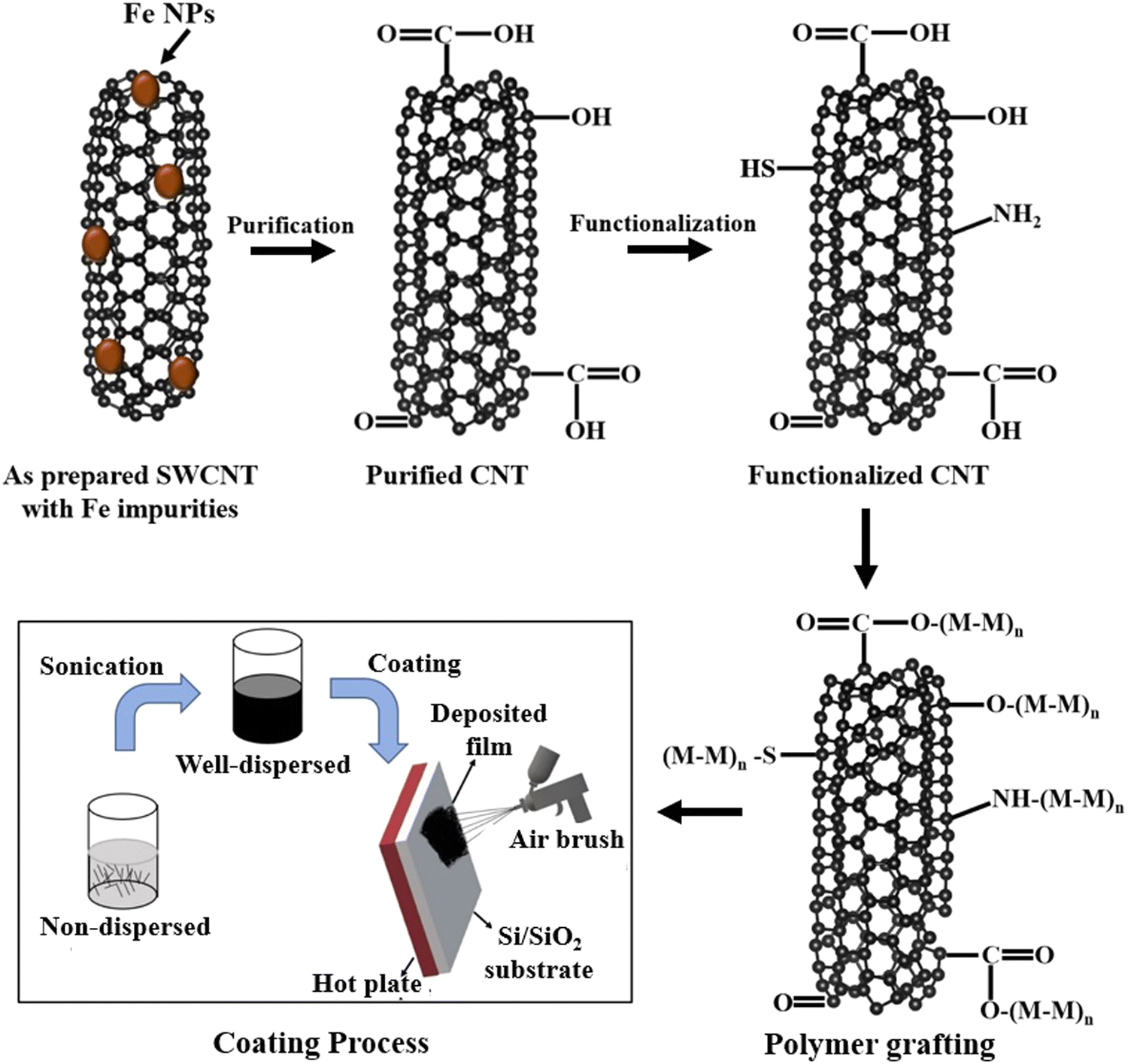 | ||
| Fig. 1 Schematic diagrams showing the inclusion of various functional groups on the side walls of the as-prepared CNTs after conducting purification, functionalization and polymer grafting. The last panel of the figure illustrates the deposition process (spray coating) to make thin films of carbon hybrids. | ||
3. Results and discussion
3.1. XPS results
XPS studies have been performed to examine the inclusion of different functional groups and their chemical composition in the purified and functionalized sample. XPS survey scans are shown in Fig. S1 (ESI†) and high resolution XPS measurements are shown in Fig. 2. Fig. 2(a)–(d) corresponds to the C 1s and O 1s core level lines of the purified and the functionalized data. The deconvoluted C 1s spectrum of the purified sample [Fig. 2(a)] exhibits features peaking at around 284.6, 285, 286, 287 and 289 eV, which we assign to C![[double bond, length as m-dash]](https://www.rsc.org/images/entities/char_e001.gif) C sp2,32 C–C sp3,33 C–O alkoxy groups,34 CO carbonyl34 or epoxy –C–O–C–35 and O–CO carboxyl groups,34,36,37 respectively. The fitted O 1s spectrum [Fig. 2(b)] of the same sample displays contributions at 531.6, 532.8 and at 534 eV that are assigned to the –CO34 functional group (531.6 eV), ether type oxygen –C–O– of COOH38 or –C–O–C– epoxy signature39 (532.8 eV), and C–OH bonds,34,40 or H2O molecules41 (534 eV) that are trapped during the synthesis process.30
C sp2,32 C–C sp3,33 C–O alkoxy groups,34 CO carbonyl34 or epoxy –C–O–C–35 and O–CO carboxyl groups,34,36,37 respectively. The fitted O 1s spectrum [Fig. 2(b)] of the same sample displays contributions at 531.6, 532.8 and at 534 eV that are assigned to the –CO34 functional group (531.6 eV), ether type oxygen –C–O– of COOH38 or –C–O–C– epoxy signature39 (532.8 eV), and C–OH bonds,34,40 or H2O molecules41 (534 eV) that are trapped during the synthesis process.30
 | ||
| Fig. 2 High-resolution XPS spectra of C 1s and O 1s lines of the (a, b) purified, and (c, d) functionalized samples. | ||
The C 1s and O 1s spectra of the functionalized sample are shown in [Fig. 2(c) and (d)]. The C 1s line exhibits six contributions at 283.9, 284.5, 285.1, 285.7, 286.2 and 286.8 eV [Fig. 2(c)]. The peak at 283.9 eV is attributed to defective and oxidized graphite and MWCNTs,42 while the 284.5 eV peak is ascribed to graphitic CC sp2 carbon.35 The maximum observed at 285.1 eV could be due to C–C sp3 or C–H,43,44 and the line at 285.7 eV could be due to C–O and C–OH functionalities or characteristic of the C–N bond with sp2 hybridization.45 The contribution at 286.2 eV is typical of carbon making a single bond with oxygen representing alkoxy group or with nitrogen [C–(O,N)]46 or with sulfur.46 The peak at 286.8 eV could be characteristic of CN47 or CS bonds48 or CO carbonyl,35 or an epoxy –C–O–C– group.36 The O 1s spectrum of the functionalized sample reveals four peak features centering around 531.6, 533.3, 535.3, and 536.8 eV after the deconvolution [Fig. 2(d)]. The first peak at 531.6 eV is assigned to –CO, COOH and N–CO,49,50 or the sulfonic group (SO3).51 The peak at 535.3 eV could be a contribution coming from O in H2O,45,52,53 and the feature at 536.8 eV could be coming from oxygen bonded to sulfur in sulfuric acid.54
3.2. Raman studies
Raman studies were performed to evaluate the chemical state by investigating the evolution of the characteristic D, G and 2D bands of the graphitic carbon and the nano carbon materials. Fig. 3(a)–(c) shows the normalized Raman spectra of the as-prepared, purified and functionalized sample. Attestation of the D, G, and 2D bands is seen clearly in the acquired Raman spectra [Fig. 3(a)–(c)], along with the characteristic radial breathing modes (RBM) unique to the SWCNTs that are observed in the as-prepared samples, and partly in the purified samples [inset of Fig. 3(a) and (b)]. A very prominent and intense RBM is evident in the as-prepared data compared to the purified spectrum, signaling the higher concentration of highly crystalline, defect-free SWCNT bundles in the raw HiPCO specimen. The signature of a very low intense D peak in the purified spectrum also signifies a low concentration of defects in the sample. The RBM of the two spectra exhibit distinctly different intensities, shapes and peak positions, indicating the structural unfolding of SWCNTs and attachment of oxygen-containing functional groups on the side walls after the acid treatment. While the intensity of the defect-induced D peak is very low for the as-prepared SWCNTs, the peak intensity gradually increases from the purified data to the functionalized data [Fig. 3]. This reveals the distortion in the graphitic structure, incorporation of foreign chemical species, and increase in the sp3 hybridization of carbon from sp2.32,34–36 The as-prepared sample exhibits a lowest ID/IG ratio [0.2], while the functionalized sample has the highest ID/IG value [0.7]. The ID/IG ratio of the purified sample lies in-between, which is 0.6. This clearly manifests a declining crystalline quality and increase of defects from raw SWCNTs to functionalized data. Emergence of a feeble shoulder-like feature observed at 1650 cm−1 in the G band of the functionalized spectrum is the characteristic of the graphitic materials with numerous defects, which additionally indicate an increased disorder and higher level of stepwise incorporation of functional moieties in the system.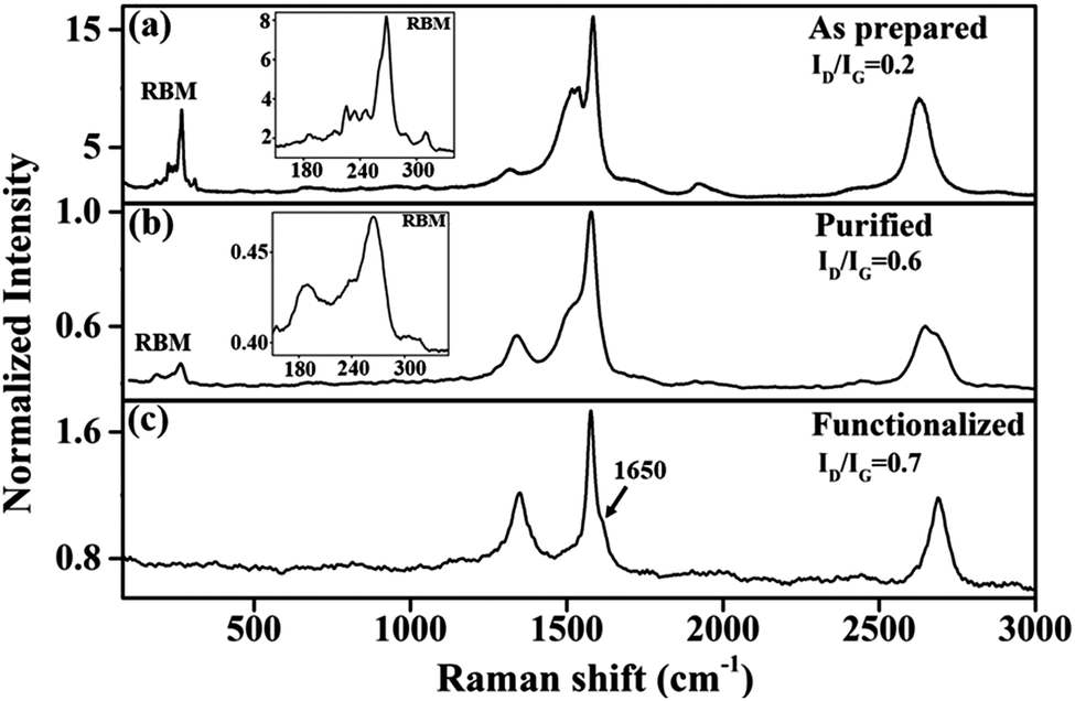 | ||
| Fig. 3 Raman spectra of (a) as-prepared, (b) purified and (c) functionalized samples. The spectra are normalized with respect to the G peak of the purified samples shown in (b). Insets of (a) and (b) reveal the RBM in the as-prepared and purified samples. | ||
3.3. TEM investigations
The performed TEM investigations are shown in Fig. 4 and Fig. S2 (ESI†). The as-prepared sample reveals SWCNT bundles, along with embedded metal particles, and evidence of sporadic amorphous carbon contaminants [Fig. S2(a), ESI†] in the SWCNT network. By comparison, after the oxidative acid purification, there is a huge reduction of Fe and amorphous contaminants [Fig. S2(b) and (c), ESI†]. High-resolution SWCNT networks can be seen in Fig. S2(c) (ESI†) after the purification process. The resultant product after the purification and functionalization process is a multi-component material with evidence of various low-dimensional carbon features [Fig. 4]. Fig. 4(a)–(d) shows the TEM micrographs obtained from the purified sample, while Fig. 4(e)–(h) displays the morphology of the functionalized data. The network of entangled and branched bundles of SWCNTs [Fig. 4(a)] is still evident. However, they are altered and distorted after oxidative treatments. The data reveal the structural degradation of SWCNT bundles to some extent, and the emergence of heterogeneous components like ‘Y’ and ‘T’ junctions [Fig. 4(a)], MWCNTs [Fig. 4(b)], GS and CNS [Fig. 4(c) and (d)] after the purification process. The formation of MWCNT from the SWCNT network [shown by arrows in Fig. 4(b)] and the folding of GS into CNS [Fig. 4(c) and (d)] can be directly seen in the TEM micrographs of the purified sample. These structural derivatives are discussed elsewhere.30,31 Additional structural evolution of the SWCNT bundles is revealed after performing the sulfo-nitric treatment in the TEM investigations of the functionalized sample [Fig. 4(e)–(h)]. Fig. 4(e) shows the SWCNT network, while Fig. 4(f) exhibits the MWCNTs in the functionalized data. Strong acid treatment of H2SO4 and HNO3 further cuts the CNS longitudinally. This is evident in Fig. 4(g), as the length of the CNS observed in the TEM micrograph is shorter compared to the CNS in the purified sample. We also observed spiral-like twisted structures of MWCNTs [Fig. 4(h)] after the sulfo-nitric process. It is documented that the HNO3 treatment of SWCNTs usually generates multi-shell phases of carbon, like MWCNTs, CNOs, etc.55 Twisted structures of collapsed SWCNTs or MWCNTs minimize the free energy in the deformed state, or establish a local minimum with a large barrier to sustain the collapsed state.56,57 Coils of MWCNTs, suspended or supported on the surfaces, are due to the competition between the interlayer attractive force and curvature elasticity, while the atomic lattice registry-dependent intertube interactions between SWCNTs of different helicity generate the twisted SWCNT ropes.56,58–62 The periodicity of the twisted nodes seen in our case is around 25 ± 5 nm [Fig. 4(h)]. These structural forms induced by curvature elasticity after the sulfo-nitric functionalization process can be very useful to achieve the large-scale deformation of nanoscale specimens, and for biopolymer applications. These twisted structures can be used as actuators, lithium-ion batteries, etc.63,64 The right panel of [Fig. 4(h)] shows the resolved fringes within the nodes of collapsed MWCNTs. High-resolution TEM micrographs of these nodes look like “CNO-like” structures, having fringes of the graphitic (002) layers stacked with a spacing of 0.34 ± 0.02 nm.65 CNOs are members of the fullerene family, comprising quasi-spherical or polyhedral-shaped graphitic layers with a hollow core.65 The structural simplicity and chemical reactivity of the CNO-like structures are very useful for applications in heterogeneous catalysis,66 electro-optical devices,67 energy storage, etc.68 The cylindrical or spherical morphology of these particles at the nanometer scale can demonstrate interesting tribological properties, which are mostly due to their shape and chemical inertness without dangling bonds. As a result, CNO-like structures are used as additives, and can lead to a strong reduction of both friction and wear even at low temperature. These particles are also considered promising candidates as solid lubricants for incorporation in fuels by NASA for aerospace applications,69 owing to their lubricating property. Onion-like structures along the tube can also be induced due to the presence of a minuscule quantity of –CHx functional groups on the side walls of the CNTs.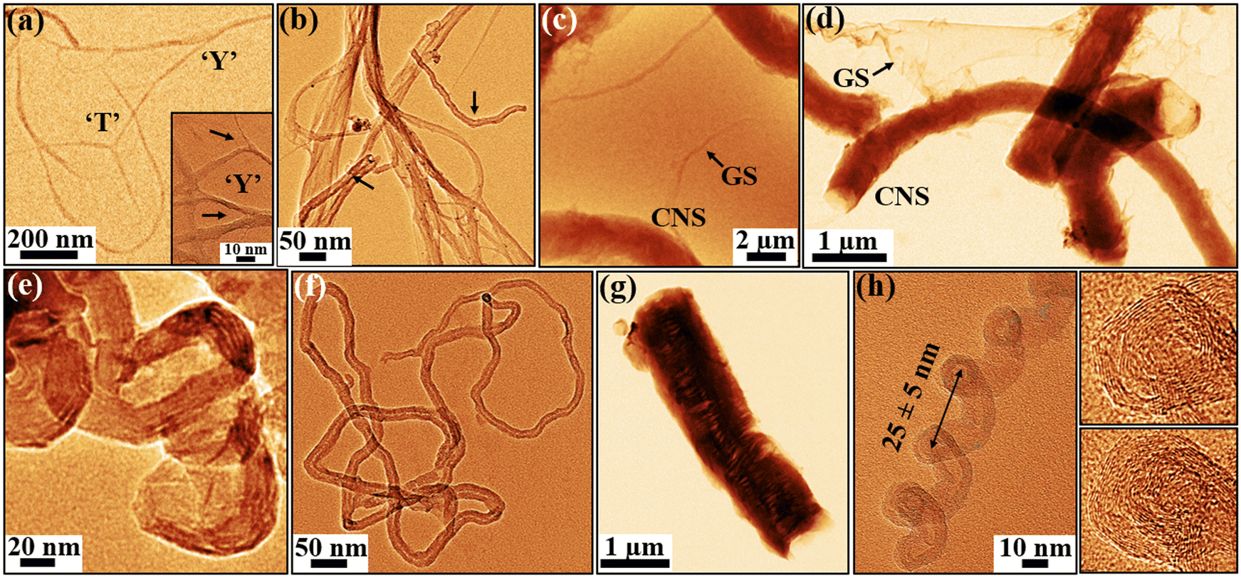 | ||
| Fig. 4 TEM investigations of the purified (a)–(d) and functionalized (e)–(h) samples with different low-dimensional structures of carbon. (a) SWCNTs forming ‘Y’ and ‘T’ like junctions after purification. Inset of (a) shows further evidence of ‘Y’ junctions marked as arrows. (b) Emergence of MWCNTs from the SWCNT bundles. MWCNTs are marked in the image. (c) and (d) GS and CNS in the purified sample. Rolling of GS to CNS can be seen. (e) SWCNT bundles in the functionalized sample with enlarged diameter due to the functionalization process.29 (f) MWCNTs, and (g) CNS in the functionalized sample. (g) Twisted structure of MWCNTs with a periodicity of 25 ± 5 nm. Right panel of (h) shows ‘CNO’-like nodes of the twisted structures with a graphitic (002) periodicity of 0.34 ± 0.02 nm of the fringes. | ||
Our stepwise acid treatments of the SWCNTs using concentrated HCl and a mixture of H2SO4 and HNO3 are supplemented by the damage to the nanotube framework via creation of intrinsic defects and holes that are functionalized with oxygenated functional groups, like carboxylic, hydroxyl, ketone, alcohol, ester, sulfate, nitrate, etc. Overall, this atomic alteration at different sites and chemical modification tend to open up the tubes, which eventually give rise to distinct structures. It is known that sulfate with a moderate solvated size and polarizability also helps in exfoliation.70 Statistically, the percentage of structural diversity in the sample was calculated by considering around 150 TEM micrographs. We find that the main components in the functionalized sample are CNS, MWCNTs, GS, and SWCNTs, contributing more than 95%. Other structural forms, like junctions, CNT coils, etc., comprise less than 5% in the sample. This is shown in Fig. 6(c). TEM micrographs also provide an estimation of the diameter of the SWCNTs, MWCNTs and CNS, which is 1–3 nm,29 20–30 nm and 500 nm to 1 μm, respectively. The typical functionalized MWCNTs consist of 15–25 layers with a graphitic (002) planar spacing of ∼0.34 nm. We cannot comment on the number of layers of CNS due to the unavailability of cross-sectional TEM evidences.
3.4. Electrical characterization
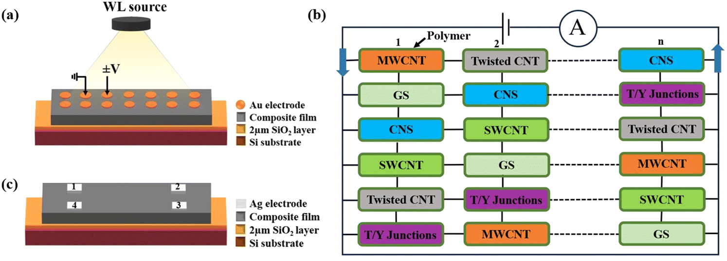 | ||
| Fig. 5 (a) Schematic representation of the two-probe electrical characterization using the Au electrode under WL illumination. (b) Possible combinations of current channels within the complex network of different carbon structural hybrids in a two-electrode measurement system. (c) Schematic of the Hall measurement in vdP geometry. | ||
Fig. 6(a) is the cross-sectional SEM image revealing the thickness of the film, which is approximately 250 ± 10 μm. Fig. 6(b) shows a TEM micrograph obtained from a 30 mg polymer sample, exhibiting a 10–20 nm thick polymer layer around the CNT structures. The concentration of different structural phases in the sample is shown in Fig. 6(c). Statistically, the CNS concentration seems to be the highest in the sample with an average weight percentage of more than 30%, followed by MWCNTs, GS and SWCNTs. The weight percentage of other structural hybrids is below 5% [Fig. 6(c)]. The I–V characteristics obtained at RT across Au electrodes on three different sets of films with the same carbon content, but different polymer aggregates (20, 25 and 30 mg), are shown in Fig. 6(d). Au electrodes were made on the sample surface using the shadow mask technique. Three independent current paths can be seen in Fig. 6(d), depending on the amount of polymer in the films. An increasing current with decreasing polymer content is clearly evident in the plots [Fig. 6(d)], indicating an enhanced resistance of the channels with the polymer increment. This is a direct manifestation of polymer-induced barriers, since the polyurethane binder used in our study is insulating. Tunneling of electrons through different structural components would largely depend on the thickness of the insulating polymer layer on them. Usually, an insulating layer of thickness of approximately 2 nm or less is desirable for the tunneling of carriers in a CNT-based system. However, metal electrodes, as well as structural diversity would play an instrumental role in amplifying the intrinsic electric field of the film that in turn would reduce the effective barrier caused by the polymer. This would help to induce tunneling within the junctions.72,73 Therefore, the polymer binder plays a significant role for the overall electrical nature of the film.
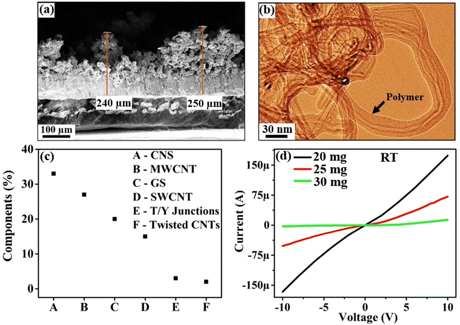 | ||
| Fig. 6 (a) Cross-sectional SEM image of a coated film with 30 mg polyurethane binder. The thickness of the film is 250 ± 10 μm. (b) TEM image of polymer-grafted CNTs revealing a polymer thickness of around 10–20 nm. (c) Statistical weight percentage of different structural components present in the sample. (d) Typical I–V characteristics exhibiting different conducting channels depending on the polymer content. | ||
Temperature-dependent I–V spectra were acquired by two-probe electrical measurements on the 30 mg polymer-coated films from 2–3 different samples of the same specifications, and are shown in Fig. 7–9. Fig. 7(a)–(c) reveals the current trend obtained under dark conditions. Fig. 7(a) depicts the typical I–V curves at RT and at 80 °C. Each spectrum in Fig. 7(a) corresponds to an average of 10 data sets that were obtained at various points on similar film(s). As can be seen, the error bar of the data points lies within the limit [Fig. 7(a)]. The RT I–V spectra exhibit a higher slope compared to the data acquired at 80 °C, clearly demonstrating a higher current at RT under dark conditions [Fig. 7(a)]. Typical plots of the natural log of current vs. voltage are shown in Fig. 7(b) and (c). In these graphs, many I–V data sets acquired under the same conditions are plotted together, confirming the consistent behaviour of the current.
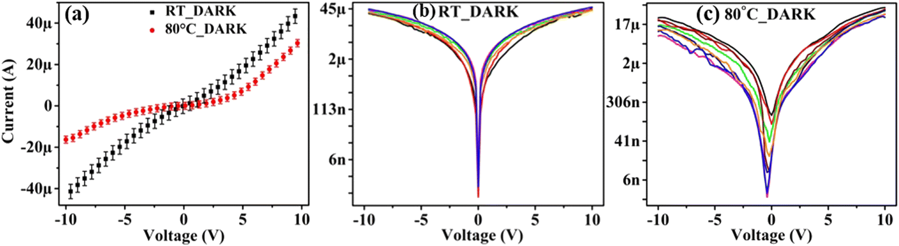 | ||
| Fig. 7 Two-probe electrical measurements at RT and 80 °C on the coated film in the dark. (a) Overall I–V characteristics. Each spectrum is an average of 10 data sets. (b) and (c) Natural log of current vs. voltage plots. There are many data sets (8–10) in each graph shown in different colours, validating the repeatability of the measurement. | ||
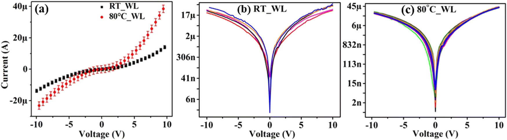 | ||
| Fig. 8 Two-probe electrical measurements at RT and 80 °C under WL exposure. (a) Overall I–V characteristics. Each curve corresponds to an average of 20 data sets. The experimental error lies within the limit. Natural log of current vs. voltage plots. There are 6 data sets in (b) and 26 data sets in (c) denoted in different colours to show the consistent electrical behaviour of the sample. | ||
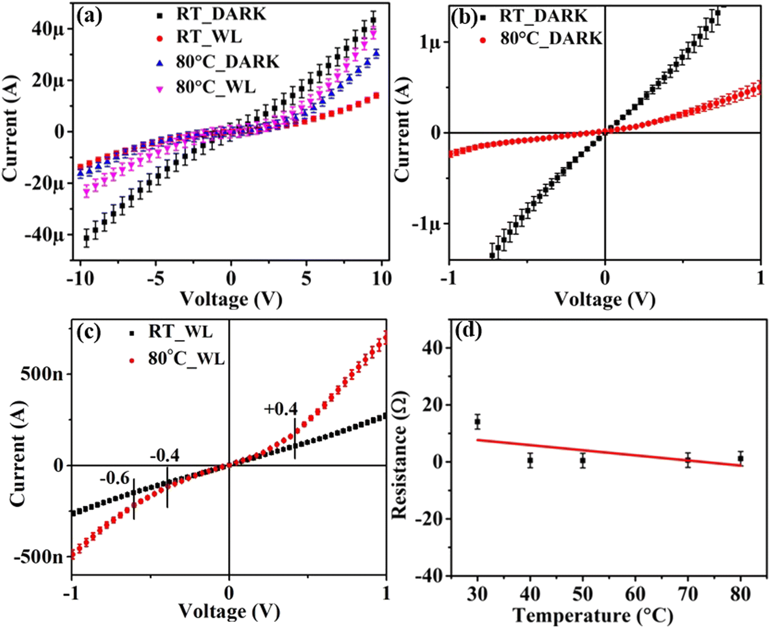 | ||
| Fig. 9 (a) Consolidated I–V plots under dark condition and WL illumination. (b) I–V characteristics under dark conditions for a voltage range of ±1 V. (c) I–V data under WL exposure for a voltage range of ±1 V. A rise in the current after certain voltages is denoted in the plot. (d) Resistance vs. temperature plot displaying the semiconducting nature of the film. | ||
Fig. 8 reveals the current characteristics at RT and 80 °C acquired under WL exposure. Each spectrum here corresponds to an average of 20 data sets. Under WL illumination, we obtain a higher current at 80 °C than RT [Fig. 8(a)–(c)], revealing an opposite trend of the current compared to the data collected in the dark. The repeatability of the I–V spectra, as well as the distinct difference in the current at RT and 80 °C, can also be observed from the plots of the natural log of currents vs. voltage shown in Fig. 8(b) and (c).
Fig. 9(a) shows the overall current characteristics of the film. Here, we have consolidated the plots shown in Fig. 7(a) and 8(a) to provide an immediate overall understanding of the current trends. As can be seen in Fig. 9(a), the RT dark current is the highest, followed by 80 °C WL, 80 °C dark and RT WL, respectively. I–V data around zero bias are shown in Fig. 9(b) and (c). The dark current observed for the voltage range ±1 V [Fig. 9(b)] is mainly due to thermionic emission and thermally-assisted tunneling of the carriers across the junctions.74,75 Under WL illumination [Fig. 9(c)], a rise in current is noticed beyond a certain voltage in both forward and reverse bias. At RT, this increase happens around +0.4, −0.6 V; while at 80 °C, it occurs at around +0.4 V, −0.4 V. This reveals a higher turn-on voltage in the negative bias for the RT current. We attribute this to the reduced thermal effects at RT than at 80 °C. The resistance vs. temperature plot is shown in Fig. 9(d). A linear fit of the data reveals a decreasing resistance with temperature, exhibiting a negative slope that emphasizes a semiconducting behaviour of the film. The temperature-dependent I–V characteristics discussed above also indicate semiconductor-based diodes or Schottky junctions that dominate our devices.74,75
The electronic processes at 80 °C under dark conditions [Fig. 7(a), (c) and 9(a), (b)] can be addressed by considering external heating that will create hot carriers in the system via electron–phonon scattering and by Joule heating. During Joule heating, the temperature of the carriers is usually more than that of the system. In a thermodynamic scenario, hot carriers will dissipate energy to a bath via carrier–carrier interaction and by other relaxation processes to attain thermal stability, giving a broad Fermi–Dirac distribution of electrons and holes.82–85 Thus, the ballistic electronic transport in the 1D and quasi-1D structures is largely affected owing to a higher rate of phonon–phonon, phonon–boundary, and phonon–defect scatterings at higher temperature. As a result, the current at 80 °C will be less compared to that at RT [Fig. 7(a), (c) and 9(a), (b)]. These results are in good agreement with the typical MWCNTs or CNT yarns that show a monotonic increase of resistance with increasing temperature.86,87
When illuminated by WL [Fig. 8 and 9(a), (c)], CNT-based composite films will absorb the electromagnetic radiation via free carrier and excitonic absorption processes.88,89 Also, the micro-cavities and pores observed on the film surface29 will trap WL inside the film, and will further enhance the absorption process. WL photons of different wavelengths and energies will interact with the electrons coupled with the vibrating phonons. Although the current path within the film is extremely complicated, as indicated in Fig. 5(b), the overall photocurrent generation will be governed by the competition between the photovoltaic effect and photothermal effect.90 At RT, carrier injection from the electrodes to the film will be dominated by thermal emission and not by tunneling, owing to large barrier height. Also, the binding energy (BE) of the photo-induced excitons is of the order of several hundred meV, which is much higher than the RT thermal energy.74 The strong interaction between the electrons and holes in the quasi 1D structures is mainly responsible for this high exciton BE, preventing the separation and collection of photo-generated electron–hole pairs. This will affect the carrier transport at RT, but not at higher temperature. As a result, the CNT-based films are immune to any change under an applied external field and exhibit a large dark current that is difficult to manipulate.91
At 80 °C, the photo-induced excitons will mostly be separated, contributing to the carrier transport dominated by thermal emission and thermally-assisted tunneling.92,93 Oscillating electrons within the carbon nanostructures will tune the Fermi level at the junctions and a photo-assisted, thermally induced tunneling will occur via electrons absorbing or emitting photons, as well as due to the excitons that are getting dissociated at 80 °C. This will give a higher current at an elevated temperature under WL, which will be evident in the I–V spectra with a temperature-dependent shift [Fig. 8 and 9(a), (c)]. However, the photo-response of the metallic nanostructures, e.g., metallic CNTs and CNS, etc. in the film will be governed by thermal effects, and not by excitonic contributions.6,89 In general, the electrical nature of this complex carbon–polymer network under light will be due to the photons absorbed through inter-band transitions, generation of free carriers via exciton dissociation at a higher temperature, and the thermal energy present in the system.
The junctions between the CNTs, CNT bundles and other structural forms, as well as the electrical characteristics of the individual structures would also significantly govern the overall electrical behaviour of the film. Junctions play a crucial role by offering resistance to the electron transport. Insufficient alignment, overlap regions and insulated polymer grafting will increase the junction resistance.92,94 In our case, the 10–20 nm thick polyurethane binder on the structural hybrids [Fig. 6(b)] will enforce an additional energy barrier to the numerous inter-structure junctions, and affect the charge hopping within the 3D composite network.95–97 The probability of non-radiative relaxations of the trapped excitons within the small structural components will also be enhanced under WL, reducing the carrier transport further98 at RT compared to 80 °C. While the SWCNTs are metallic or semiconducting, MWCNTs with a large number of walls exhibit electrical properties of graphite, and those with fewer walls are mostly semiconducting in nature.99 GS are either metallic or semiconducting, depending on the edges.100 It is reported that for CNOs, the multi-layered carbon arrays yield large capacitance effects, a property related to charge storage.101 The electrical nature of the twisted CNTs is hardly known. CNS are good conductors with low resistance and weak gate dependence.99 CNS with zigzag edges are metallic,99 while armchair edges exhibit very small or zero bandgap.101 The electrical nature of junctions like ‘Y’ or ‘T’ will mostly be governed by the Schottky junction behavior.102 The main structural components present in our sample are CNTs, GS and CNS, which primarily dominate the electrical nature of the film. First-principles simulations and the introduction of machine learning interatomic potentials to ab initio data sets carried out on 2D graphene and graphene heterostructures, etc. could explain various physical properties of these systems quantitatively.103,104 We plan similar studies in the future to obtain further insight into our complex carbon–polymer films. It is also reported that typical CNT films with a thickness of 10 μm or more act as a black body absorber, and reveal the poor electronic transport with high dark current and reduced ON/OFF ratios under incident light.91,105,106 Our results with different structural components of carbon, including CNTs, are in good agreement with these studies.
3.5. Hall measurements
We have also carried out RT Hall measurements to understand the overall electrical nature of the film. Results obtained from Hall studies are summarized in Table 1. Measurements reveal an n-type carrier with a density (ns) of 3.1 × 1013 cm−2, mobility (μ) of 1.5 × 102 cm2 V−1 s−1 and an overall film resistance (Rs) of 1.1 × 10³ Ω. This resistance value shows that the film is semiconducting in nature, further corroborating the two-probe measurements discussed earlier. Here, it should be noted that due to the existence of hopping conductions in disordered semiconductors such as CNTs and conjugated polymer films, the Hall measurements might provide overestimated numbers of carrier density, etc.107,108 However, Hall studies were carried out to find a qualitative estimation and to cross-check the overall electrical nature of the film. The results obtained from the Hall measurements agree well with the two-probe studies, providing the necessary insight into the electrical nature of the random network of composite carbon film comprising a wide range of 1D, 2D structural derivatives.| Charge carrier density (ns) | Sheet resistance (Rs) | Hall mobility (μ) |
|---|---|---|
| 3.1 × 1013 cm−2 | 1.1 × 10³ Ω | 1.5 × 102 cm2 V−1 s−1 |
4. Conclusion
Various low-dimensional structural derivatives of carbon, e.g., MWCNTs, GS, CNS, twisted CNTs, CNO like structures, ‘Y’ and ‘T’ junctions, are realized from HiPCO SWCNT bundles. These heterogeneous components have emerged during oxidative acid purification and sulfonitric functionalization treatments of the as-prepared SWCNTs. We identify different O, N and S containing functional groups, whose attachments have contributed partly to the formation of different structural forms of 1D, 2D carbon in abundance. These covalently functionalized multi-component carbon hybrids, along with the polyurethane conjugate in a random network unravel the semiconducting electrical nature of the film. These results pave the way for integrating heterogeneous low-dimensional materials of carbon to illustrate the novel functionalities that work beyond the individual homogeneous materials properties. We propose a facile cost-effective way to fabricate sustainable and stable all-carbon thin film coatings and study the electrical nature, which can have potential applications in electronics to biology, energy conversion and storage, sensing, etc.Data availability
Data are available on request.Conflicts of interest
There are no conflicts to declare.Acknowledgements
K. B. is sincerely thankful to the DST Mobility Fellowship for providing necessary personal and professional stability, and funding for overall support.References
- A. D. Franklin, The road to carbon nanotube transistors, Nature, 2013, 498, 443–444, DOI:10.1038/498443a.
- T. Uchino, G. Ayre, D. C. Smith, J. L. Hutchison, C. H. de Groot and P. Ashburn, Metal-Catalyst-Free Growth of Carbon Nanotubes and Their Application in Field-Effect Transistors, Electrochem. Solid-State Lett., 2011, 14, K21, DOI:10.1149/1.3534829.
- S. Wang, Q. Zeng, L. Yang, Z. Zhang, Z. Wang, T. Pei, L. Ding, X. Liang, M. Gao, Y. Li and L.-M. Peng, High-Performance Carbon Nanotube Light-Emitting Diodes with Asymmetric Contacts, Nano Lett., 2011, 11, 23–29, DOI:10.1021/nl101513z.
- E. Shi, L. Zhang, Z. Li, P. Li, Y. Shang, Y. Jia, J. Wei, K. Wang, H. Zhu, D. Wu, S. Zhang and A. Cao, TiO2-Coated Carbon Nanotube-Silicon Solar Cells with Efficiency of 15, Sci. Rep., 2012, 2, 884, DOI:10.1038/srep00884.
- Z. Li, V. P. Kunets, V. Saini, Y. Xu, E. Dervishi, G. J. Salamo, A. R. Biris and A. S. Biris, SOCl 2 enhanced photovoltaic conversion of single wall carbon nanotube/n-silicon heterojunctions, Appl. Phys. Lett., 2008, 93, 2006–2009, DOI:10.1063/1.3050465.
- Z. Li, V. Saini, S. E. Bourdo, L. Zheng, E. Dervishi and A. S. Biris, Photovoltaic Devices Based on Single Wall Carbon Nanotubes, MRS Proc., 2009, 1210, 1210-Q04-06, DOI:10.1557/PROC-1210-Q04-06.
- K. Besteman, J. Lee, F. G. M. Wiertz, H. A. Heering and C. Dekker, Enzyme-Coated Carbon Nanotubes as Single-Molecule Biosensors, Nano Lett., 2003, 3, 727–730, DOI:10.1021/nl034139u.
- F. Kreupl, A. Graham, G. Duesberg, W. Steinhögl, M. Liebau, E. Unger and W. Hönlein, Carbon nanotubes in interconnect applications, Microelectron. Eng., 2002, 64, 399–408, DOI:10.1016/S0167-9317(02)00814-6.
- M. M. Waldrop, The chips are down for Moore's law, Nature, 2016, 530, 144–147, DOI:10.1038/530144a.
- M. M. Shulaker, G. Hills, N. Patil, H. Wei, H.-Y. Chen, H.-S. P. Wong and S. Mitra, Carbon nanotube computer, Nature, 2013, 501, 526–530, DOI:10.1038/nature12502.
- Y. Liu, S. Wang, H. Liu and L.-M. Peng, Carbon nanotube-based three-dimensional monolithic optoelectronic integrated system, Nat. Commun., 2017, 8, 15649, DOI:10.1038/ncomms15649.
- H. Li, Y. Shi and L.-J. Li, Synthesis and optoelectronic applications of graphene/transition metal dichalcogenides flat-pack assembly, Carbon, 2018, 127, 602–610, DOI:10.1016/j.carbon.2017.11.030.
- L. Yang, S. Wang, Q. Zeng, Z. Zhang, T. Pei, Y. Li and L.-M. Peng, Efficient photovoltage multiplication in carbon nanotubes, Nat. Photonics, 2011, 5, 672–676, DOI:10.1038/nphoton.2011.250.
- D. Capista, L. Lozzi, A. Di Bartolomeo, F. Giubileo, N. Martucciello and M. Passacantando, SWCNT-Si photodetector with voltage-dependent active surface, Nano Express, 2024, 5(1), 015004, DOI:10.1088/2632-959X/ad12d9.
- A. Di Bartolomeo, F. Giubileo, A. Grillo, G. Luongo, L. Iemmo, F. Urban, L. Lozzi, D. Capista, M. Nardone and M. Passacantando, Bias tunable photocurrent in metal-insulator-semiconductor heterostructures with photoresponse enhanced by carbon nanotubes, Nanomaterials, 2019, 9, 29–31, DOI:10.3390/nano9111598.
- L. P. Simoneau, J. Villeneuve, C. M. Aguirre, R. Martel, P. Desjardins and A. Rochefort, Influence of statistical distributions on the electrical properties of disordered and aligned carbon nanotube networks, J. Appl. Phys., 2013, 114, 28–30, DOI:10.1063/1.4821885.
- Y. Wu, X. Zhao, Y. Shang, S. Chang, L. Dai and A. Cao, Application-Driven Carbon Nanotube Functional Materials, ACS Nano, 2021, 15, 7946–7974, DOI:10.1021/acsnano.0c10662.
- J. W. Singleton, G. R. Cobb, H. E. Misak and R. A. Kemnitz, Quantifying the electrical behavior of carbon nanotube sheet enhanced with acid functionalization and polymer intercalation, Results Mater., 2020, 5, 100059, DOI:10.1016/j.rinma.2020.100059.
- Y. S. Song and J. R. Youn, Influence of dispersion states of carbon nanotubes on physical properties of epoxy nanocomposites, Carbon, 2005, 43, 1378–1385, DOI:10.1016/j.carbon.2005.01.007.
- M. C. LeMieux, M. Roberts, S. Barman, W. J. Yong, M. K. Jong and Z. Bao, Self-sorted, aligned nanotube networks for thin-film transistors, Science, 2008, 321, 101–104, DOI:10.1126/science.1156588.
- M. D. Lay, J. P. Novak and E. S. Snow, Simple route to large-scale ordered arrays of liquid-deposited carbon nanotubes, Nano Lett., 2004, 4, 603–606, DOI:10.1021/nl035233d.
- E. S. Snow, J. P. Novak, P. M. Campbell and D. Park, Random networks of carbon nanotubes as an electronic material, Appl. Phys. Lett., 2003, 82, 2145–2147, DOI:10.1063/1.1564291.
- E. Artukovic, M. Kaempgen, D. S. Hecht, S. Roth and G. Grüner, Transparent and flexible carbon nanotube transistors, Nano Lett., 2005, 5, 757–760, DOI:10.1021/nl050254o.
- D. B. Shinde, M. Majumder and V. K. Pillai, Counter-ion Dependent, Longitudinal Unzipping of Multi-Walled Carbon Nanotubes to Highly Conductive and Transparent Graphene Nanoribbons, Sci. Rep., 2015, 4, 4363, DOI:10.1038/srep04363.
- P. X. Hou, C. Liu and H. M. Cheng, Purification of carbon nanotubes, Carbon, 2008, 46, 2003–2025, DOI:10.1016/j.carbon.2008.09.009.
- H. Hu, B. Zhao, M. E. Itkis and R. C. Haddon, Nitric Acid Purification of Single-Walled Carbon Nanotubes, J. Phys. Chem. B, 2003, 107, 13838–13842, DOI:10.1021/jp035719i.
- S. Saini, S. Reshmi, G. M. Gouda and K. Bhattacharjee, Emergence of carbon nanoscrolls from single walled carbon nanotubes: an oxidative route, Phys. Chem. Chem. Phys., 2021, 23, 27437–27448, 10.1039/d1cp03945h.
- F. Rivadulla, C. Mateo-Mateo and M. A. Correa-Duarte, Layer-by-Layer Polymer Coating of Carbon Nanotubes, J. Am. Chem. Soc., 2010, 132, 3751–3755, DOI:10.1021/ja910572b.
- S. Saini, S. Reshmi, G. M. Gouda, S. A. Kumar, K. V. Sriram and K. Bhattacharjee, Low reflectance of carbon nanotube and nanoscroll-based thin film coatings: a case study, Nanoscale Adv., 2021, 3, 3184–3198, 10.1039/d0na01058h.
- J. M. Moon, K. H. An, Y. H. Lee, Y. S. Park, D. J. Bae and G. S. Park, High-yield purification process of singlewalled carbon nanotubes, J. Phys. Chem. B, 2001, 105, 5677–5681, DOI:10.1021/jp0102365.
- W. Francisco, F. V. Ferreira, E. V. Ferreira, L. de S. Cividanes, A. dos R. Coutinho and G. P. Thim, Functionalization of multi-walled carbon nanotube and mechanical property of epoxy-based nanocomposite, J. Aerosp. Technol. Manage., 2015, 7, 289–293, DOI:10.5028/jatm.v7i3.485.
- Y. Xing, L. Li, C. C. Chusuei and R. V. Hull, Sonochemical oxidation of multiwalled carbon nanotubes, Langmuir, 2005, 21, 4185–4190, DOI:10.1021/la047268e.
- K. C. Chang, W. F. Ji, M. C. Lai, Y. R. Hsiao, C. H. Hsu, T. L. Chuang, Y. Wei, J. M. Yeh and W. R. Liu, Synergistic effects of hydrophobicity and gas barrier properties on the anticorrosion property of PMMA nanocomposite coatings embedded with graphene nanosheets, Polym. Chem., 2014, 5, 1049–1056, 10.1039/c3py01178j.
- R. Maiti, A. Midya, C. Narayana and S. K. Ray, Tunable optical properties of graphene oxide by tailoring the oxygen functionalities using infrared irradiation, Nanotechnology, 2014, 25, 495704, DOI:10.1088/0957-4484/25/49/495704.
- W. Sun, Z. Liu, C. Jiang, Y. Xue, W. Chu and X. Zhao, Experimental and theoretical investigation on the interaction between palladium nanoparticles and functionalized carbon nanotubes for Heck synthesis, Catal. Today, 2013, 212, 206–214, DOI:10.1016/j.cattod.2012.09.024.
- Z. Yang, H. Peng, W. Wang and T. Liu, Crystallization behavior of poly(ε-caprolactone)/layered double hydroxide nanocomposites, J. Appl. Polym. Sci., 2010, 116, 2658–2667, DOI:10.1002/app.
- G. Zhou, D. W. Wang, L. C. Yin, N. Li, F. Li and H. M. Cheng, Oxygen bridges between nio nanosheets and graphene for improvement of lithium storage, ACS Nano, 2012, 6, 3214–3223, DOI:10.1021/nn300098m.
- E. Desimoni, G. I. Casella, A. Morone and A. M. Salvi, XPS determination of oxygen-containing functional groups on carbon-fibre surfaces and the cleaning of these surfaces, Surf. Interface Anal., 1990, 15, 627–634, DOI:10.1002/sia.740151011.
- Y. J. Xu, R. Arrigo, X. Liu and D. S. Su, Characterization and use of functionalized carbon nanotubes for the adsorption of heavy metal anions, Xinxing Tan Cailiao, 2011, 26, 57–62, DOI:10.1016/S1872-5805(11)60066-8.
- B. Lesiak, L. Kövér, J. Tóth, J. Zemek, P. Jiricek, A. Kromka and N. Rangam, C sp 2/sp 3 hybridisations in carbon nanomaterials – XPS and (X)AES study, Appl. Surf. Sci., 2018, 452, 223–231, DOI:10.1016/j.apsusc.2018.04.269.
- S. C. Ray, N. Soin, T. Makgato, C. H. Chuang, W. F. Pong, S. S. Roy, S. K. Ghosh, A. M. Strydom and J. A. McLaughlin, Graphene supported graphone/graphane bilayer nanostructure material for spintronics, Sci. Rep., 2014, 4(1), 3862, DOI:10.1038/srep03862.
- J. Lomon, P. Chaiyabin, T. Saisopa, K. Seawsakul, N. Saowiang, K. Promsakha, P. Poolcharuansin, N. Pasaja, A. Chingsungnoen, R. Supruangnet, N. Chanlek, H. Nakajima and P. Songsiriritthigul, XPS and XAS preliminary studies of diamond-like carbon films prepared by HiPIMS technique, J. Phys.: Conf. Ser., 2018, 1144(1), 012048, DOI:10.1088/1742-6596/1144/1/012048.
- J. V. Rojas, M. Toro-Gonzalez, M. C. Molina-Higgins and C. E. Castano, Facile radiolytic synthesis of ruthenium nanoparticles on graphene oxide and carbon nanotubes, Mater. Sci. Eng., B, 2016, 205, 28–35, DOI:10.1016/j.mseb.2015.12.005.
- H. Maachou, M. J. Genet, D. Aliouche, C. C. Dupont-Gillain and P. G. Rouxhet, XPS analysis of chitosan-hydroxyapatite biomaterials: From elements to compounds, Surf. Interface Anal., 2013, 45, 1088–1097, DOI:10.1002/sia.5229.
- G. Beshkov, D. B. Dimitrov, S. Georgiev, D. Juan-Cheng, P. Petrov, N. Velchev and V. Krastev, XPS spectra of thin CNx films prepared by chemical vapor deposition, Diamond Relat. Mater., 1999, 8, 591–594, DOI:10.1016/s0925-9635(98)00269-6.
- S. Li, X. Song, X. Kuai, W. Zhu, K. Tian, X. Li, M. Chen, S. Chou, J. Zhao and L. Gao, A nanoarchitectured Na6Fe5(SO4)8/CNTs cathode for building a low-cost 3.6 v sodium-ion full battery with superior sodium storage, J. Mater. Chem. A, 2019, 7, 14656–14669, 10.1039/c9ta03089a.
- V. Duc Chinh, G. Speranza, C. Migliaresi, N. Van Chuc, V. Minh Tan and N. T. Phuong, Synthesis of Gold Nanoparticles Decorated with Multiwalled Carbon Nanotubes (Au-MWCNTs) via Cysteaminium Chloride Functionalization, Sci. Rep., 2019, 9, 1–9, DOI:10.1038/s41598-019-42055-7.
- U. Gelius, B. Roos and P. Siegbahn, Ab initio MO SCF calculations of ESCA shifts in sulphur-containing molecules, Chem. Phys. Lett., 1970, 4, 471–475, DOI:10.1016/0009-2614(70)85018-7.
- K. Artyushkova and P. Atanassov, X-Ray Photoelectron Spectroscopy for Characterization of Bionanocomposite Functional Materials for Energy-Harvesting Technologies, Chem. Phys. Chem., 2013, 14, 2071–2080, DOI:10.1002/cphc.201300037.
- A. Gharbi, T. Legigan, V. Humblot, S. Papot and J. M. Berjeaud, Surface functionalization by covalent immobilization of an innovative carvacrol derivative to avoid fungal biofilm formation, AMB Express, 2015, 5, 1–12, DOI:10.1186/s13568-014-0091-2.
- Q. Wang, C. Zhang, G. Shen, H. Liu, H. Fu and D. Cui, Fluorescent carbon dots as an efficient siRNA nanocarrier for its interference therapy in gastric cancer cells, J. Nanobiotechnol., 2014, 12, 1–12, DOI:10.1186/s12951-014-0058-0.
- R. F. Araújo, M. F. Proença, C. J. Silva, M. C. Paiva, S. Villar-Rodil and J. M. D. Tascón, The solvent effect on the sidewall functionalization of multi-walled carbon nanotubes with maleic anhydride, Carbon, 2014, 78, 401–414, DOI:10.1016/j.carbon.2014.07.019.
- L. Z. Qin, Y. Z. Lin, Y. C. Dou, Y. J. Yang, K. Li, T. Li and F. T. Liu, Toward enhanced photocatalytic activity of graphite carbon nitride through rational design of noble metal-free dual cocatalysts, Nanoscale, 2020, 12, 13829–13837, 10.1039/c9nr10044j.
- Y. J. Tang, Y. Wang, X. L. Wang, S. L. Li, W. Huang, L. Z. Dong, C. H. Liu, Y. F. Li and Y. Q. Lan, Molybdenum Disulfide/Nitrogen-Doped Reduced Graphene Oxide Nanocomposite with Enlarged Interlayer Spacing for Electrocatalytic Hydrogen Evolution, Adv. Energy Mater., 2016, 6, 1–7, DOI:10.1002/aenm.201600116.
- C. H. Kiang, W. A. Goddard, R. Beyers and D. S. Bethune, Structural modification of single-layer carbon nanotubes with an electron beam, J. Phys. Chem., 1996, 100, 3749–3752, DOI:10.1021/jp952636w.
- N. G. Chopra, L. X. Benedict, V. H. Crespi, M. L. Cohen, S. G. Louie and A. Zettl, Fully collapsed carbon nanotubes, Nature, 1995, 377, 135–138, DOI:10.1038/377135a0.
- L. X. Benedict, N. G. Chopra, M. L. Cohen, A. Zettl, S. G. Louie and V. H. Crespi, Microscopic determination of the interlayer binding energy in graphite, Chem. Phys. Lett., 1998, 286, 490–496, DOI:10.1016/S0009-2614(97)01466-8.
- M. F. Yu, M. J. Dyer, J. Chen, D. Qian, W. K. Liu and R. S. Ruoff, Locked twist in multiwalled carbon-nanotube ribbons, Phys. Rev. B: Condens. Matter Mater. Phys., 2001, 64, 2414031, DOI:10.1103/physrevb.64.241403.
- O. Y. Zhong-can, Z. Bin Su and C. L. Wang, Coil formation in multishell carbon nanotubes: Competition between curvature elasticity and interlayer adhesion, Phys. Rev. Lett., 1997, 78, 4055–4058, DOI:10.1103/PhysRevLett.78.4055.
- W. Clauss, D. Bergeron and A. Johnson, Atomic resolution STM imaging of a twisted single-wall carbon nanotube, Phys. Rev. B: Condens. Matter Mater. Phys., 1998, 58, R4266–R4269, DOI:10.1103/PhysRevB.58.R4266.
- Y. K. Kwon and D. Tománek, Orientational melting in carbon nanotube ropes, Phys. Rev. Lett., 2000, 84, 1483–1486, DOI:10.1103/PhysRevLett.84.1483.
- H. Inoue, T. Yoshiyama, M. Hada, D. Chujo, Y. Saito, T. Nishikawa, Y. Yamashita, W. Takarada, H. Matsumoto and Y. Hayashi, High-performance structure of a coil-shaped soft-actuator consisting of polymer threads and carbon nanotube yarns, AIP Adv., 2018, 8(7), 075316, DOI:10.1063/1.5033487.
- O. Mykhailiv, H. Zubyk and M. E. Plonska-Brzezinska, Carbon nano-onions: Unique carbon nanostructures with fascinating properties and their potential applications, Inorg. Chim. Acta, 2017, 468, 49–66, DOI:10.1016/j.ica.2017.07.021.
- N. Keller, N. I. Maksimova, V. V. Roddatis, M. Schur, G. Mestl, Y. V. Butenko, V. L. Kuznetsov and R. Schlögl, The catalytic use of onion-like carbon materials for styrene synthesis by oxidative dehydrogenation of ethylbenzene, Angew. Chem., Int. Ed., 2002, 41, 1885–1888, DOI:10.1002/1521-3773(20020603)41:11<1885::AID-ANIE1885>3.0.CO;2-5.
- N. Keller, N. I. Maksimova, V. V. Roddatis, M. Schur, G. Mestl, Y. V. Butenko, V. L. Kuznetsov and R. Schlögl, Zwiebelförmige Kohlenstoffe als Katalysatoren Dehydrierung von Ethylbenzol, Angew. Chem., 2002, 1962–1966 CrossRef.
- N. Sano, H. Wang, I. Alexandrou, M. Chhowalla, K. B. K. Teo, G. A. J. Amaratunga and K. Iimura, Properties of carbon onions produced by an arc discharge in water, J. Appl. Phys., 2002, 92, 2783–2788, DOI:10.1063/1.1498884.
- C. T. Cioffi, A. Palkar, F. Melin, A. Kumbhar, L. Echegoyen, M. Melle-Franco, F. Zerbetto, G. M. A. Rahman, C. Ehli, V. Sgobba, D. M. Guldi and M. Prato, A Carbon nano-onion-ferrocene donor-acceptor system: Synthesis, characterization and properties, Chem. - Eur. J., 2009, 15, 4419–4427, DOI:10.1002/chem.200801818.
- B. Pradhan, K. Setyowati, H. Liu, D. H. Waldeck and J. Chen, Carbon nanotube-polymer nanocomposite infrared sensor, Nano Lett., 2008, 8, 1142–1146, DOI:10.1021/nl0732880.
- S. J. Wind, J. Appenzeller and P. Avouris, Lateral Scaling in Carbon-Nanotube Field-Effect Transistors, Phys. Rev. Lett., 2003, 91, 1–4, DOI:10.1103/PhysRevLett.91.058301.
- C. Bower, A. Kleinhammes, Y. Wu and O. Zhou, Intercalation and partial exfoliation of single-walled carbon nanotubes by nitric acid, Chem. Phys. Lett., 1998, 288, 481–486, DOI:10.1016/S0009-2614(98)00278-4.
- R. Sreedharan, M. Mohan, S. Saini, A. Roy and K. Bhattacharjee, Intermediate Cu-O-Si Phase in the Cu-SiO 2/Si(111) System: Growth, Elemental, and Electrical Studies, ACS Omega, 2021, 6, 23826–23836, DOI:10.1021/acsomega.1c02646.
- X. Xu and G. R. Brandes, A method for fabricating large-area, patterned, carbon nanotube field emitters, Appl. Phys. Lett., 1999, 74, 2549–2551, DOI:10.1063/1.123894.
- A. Sharma, V. Singh, T. L. Bougher and B. A. Cola, A carbon nanotube optical rectenna, Nat. Nanotechnol., 2015, 10, 1027–1032, DOI:10.1038/nnano.2015.220.
- J. Appenzeller, M. Radosavljević, J. Knoch and P. Avouris, Tunneling Versus Thermionic Emission in One-Dimensional Semiconductors, Phys. Rev. Lett., 2004, 92, 048301, DOI:10.1103/PhysRevLett.92.048301.
- P. Avouris, Carbon Nanotube Electronics and Optoelectronics, MRS Bull., 2004, 29, 403–410, DOI:10.1557/mrs2004.123.
- J. Huang, A. L. Ng, Y. Piao, C.-F. Chen, A. A. Green, C.-F. Sun, M. C. Hersam, C. S. Lee and Y. Wang, Covalently Functionalized Double-Walled Carbon Nanotubes Combine High Sensitivity and Selectivity in the Electrical Detection of Small Molecules, J. Am. Chem. Soc., 2013, 135, 2306–2312, DOI:10.1021/ja310844u.
- B. R. Goldsmith, J. G. Coroneus, A. A. Kane, G. A. Weiss and P. G. Collins, Monitoring single-molecule reactivity on a carbon nanotube, Nano Lett., 2008, 8, 189–194, DOI:10.1021/nl0724079.
- B. R. Goldsmith, J. G. Coroneus, V. R. Khalap, A. A. Kane, G. A. Weiss and P. G. Collins, Conductance-Controlled Point Functionalization of Single-Walled Carbon Nanotubes, Science, 2007, 315, 77–81, DOI:10.1126/science.1135303.
- L. Prisbrey, D. Roundy, K. Blank, L. S. Fifield and E. D. Minot, Electrical characteristics of carbon nanotube devices prepared with single oxidative point defects, J. Phys. Chem. C, 2012, 116, 1961–1965, DOI:10.1021/jp208870c.
- M. K. Ashraf, N. A. Bruque, R. R. Pandey, P. G. Collins and R. K. Lake, Effect of localized oxygen functionalization on the conductance of metallic carbon nanotubes, Phys. Rev. B: Condens. Matter Mater. Phys., 2009, 79, 115428, DOI:10.1103/PhysRevB.79.115428.
- H. J. Choi, J. Ihm, S. G. Louie and M. L. Cohen, Defects, quasibound states, and quantum conductance in metallic carbon nanotubes, Phys. Rev. Lett., 2000, 84, 2917–2920, DOI:10.1103/PhysRevLett.84.2917.
- K. L. Grosse, M.-H. Bae, F. Lian, E. Pop and W. P. King, Nanoscale Joule heating, Peltier cooling and current crowding at graphene–metal contacts, Nat. Nanotechnol., 2011, 6, 287–290, DOI:10.1038/nnano.2011.39.
- W. Yang, S. Berthou, X. Lu, Q. Wilmart, A. Denis, M. Rosticher, T. Taniguchi, K. Watanabe, G. Fève, J.-M. Berroir, G. Zhang, C. Voisin, E. Baudin and B. Plaçais, A graphene Zener–Klein transistor cooled by a hyperbolic substrate, Nat. Nanotechnol., 2018, 13, 47–52, DOI:10.1038/s41565-017-0007-9.
- M. Freitag, M. Steiner, Y. Martin, V. Perebeinos, Z. Chen, J. C. Tsang and P. Avouris, Energy Dissipation in Graphene Field-Effect Transistors, Nano Lett., 2009, 9, 1883–1888, DOI:10.1021/nl803883h.
- M. Freitag, H.-Y. Chiu, M. Steiner, V. Perebeinos and P. Avouris, Thermal infrared emission from biased graphene, Nat. Nanotechnol., 2010, 5, 497–501, DOI:10.1038/nnano.2010.90.
- D. Mattia, M. P. Rossi, B. M. Kim, G. Korneva, H. H. Bau and Y. Gogotsi, Effect of Graphitization on the Wettability and Electrical Conductivity of CVD-Carbon Nanotubes and Films, J. Phys. Chem. B, 2006, 110, 9850–9855, DOI:10.1021/jp061138s.
- J. F. Niven, M. B. Johnson, S. M. Juckes, M. A. White, N. T. Alvarez and V. Shanov, Influence of annealing on thermal and electrical properties of carbon nanotube yarns, Carbon, 2016, 99, 485–490, DOI:10.1016/j.carbon.2015.12.014.
- P. Avouris, M. Freitag and V. Perebeinos, Carbon-nanotube photonics and optoelectronics, Nat. Photonics, 2008, 2, 341–350, DOI:10.1038/nphoton.2008.94.
- M. Barkelid and V. Zwiller, Photocurrent generation in semiconducting and metallic carbon nanotubes, Nat. Photonics, 2014, 8, 47–51, DOI:10.1038/nphoton.2013.311.
- T. S. Gspann, S. M. Juckes, J. F. Niven, M. B. Johnson, J. A. Elliott, M. A. White and A. H. Windle, High thermal conductivities of carbon nanotube films and micro-fibres and their dependence on morphology, Carbon, 2017, 114, 160–168, DOI:10.1016/j.carbon.2016.12.006.
- X. Xia, S. Zhou, Y. Wang and Z. Zhang, Emerging optoelectronic architectures in carbon nanotube photodetector technologies, Fundam. Res., 2023 DOI:10.1016/j.fmre.2023.11.001.
- M. Grundmann, The Physics of Semiconductors, Springer International Publishing, Cham, 2016 DOI:10.1007/978-3-319-23880-7.
- B. E. Kilbride, J. N. Coleman, J. Fraysse, P. Fournet, M. Cadek, A. Drury, S. Hutzler, S. Roth and W. J. Blau, Experimental observation of scaling laws for alternating current and direct current conductivity in polymer-carbon nanotube composite thin films, J. Appl. Phys., 2002, 92, 4024–4030, DOI:10.1063/1.1506397.
- B. R. Sankapal, K. Setyowati, J. Chen and H. Liu, Electrical properties of air-stable, iodine-doped carbon-nanotube-polymer composites, Appl. Phys. Lett., 2007, 91, 10–13, DOI:10.1063/1.2801353.
- E. K. Sichel, J. I. Gittleman and P. Sheng, Transport properties of the composite material carbon-poly(vinyl chloride), Phys. Rev. B: Condens. Matter Mater. Phys., 1978, 18, 5712–5716, DOI:10.1103/PhysRevB.18.5712.
- E. Kymakis and G. A. J. Amaratunga, Single-wall carbon nanotube/conjugated polymer photovoltaic devices, Appl. Phys. Lett., 2002, 80, 112–114, DOI:10.1063/1.1428416.
- Z. Xu, Y. Wu, B. Hu, I. N. Ivanov and D. B. Geohegan, Carbon nanotube effects on electroluminescence and photovoltaic response in conjugated polymers, Appl. Phys. Lett., 2005, 87, 1–3, DOI:10.1063/1.2152113.
- X. He, F. Léonard and J. Kono, Uncooled Carbon Nanotube Photodetectors, Adv. Opt. Mater., 2015, 3, 989–1011, DOI:10.1002/adom.201500237.
- X. Xie, L. Ju, X. Feng, Y. Sun, R. Zhou, K. Liu, S. Fan, Q. Li and K. Jiang, Controlled Fabrication of High-Quality Carbon Nanoscrolls from Monolayer Graphene, Nano Lett., 2009, 9, 2565–2570, DOI:10.1021/nl900677y.
- A. Kukovecz, C. Kramberger, M. Holzinger, H. Kuzmany, J. Schalko, M. Mannsberger and A. Hirsch, On the stacking behavior of functionalized single-wall carbon nanotubes, J. Phys. Chem. B, 2002, 106, 6374–6380, DOI:10.1021/jp014019f.
- Y. Chen, J. Lu and Z. Gao, Structural and electronic study of nanoscrolls rolled up by a single graphene sheet, J. Phys. Chem. C, 2007, 111, 1625–1630, DOI:10.1021/jp066030r.
- I. H. Lee, S. Jun, H. Kim, S. Y. Kim and Y. Lee, Adatom-assisted structural transformations of fullerenes, Appl. Phys. Lett., 2006, 88(1), 011913, DOI:10.1063/1.2161175.
- B. Mortazavi, B. Javvaji, F. Shojaei, T. Rabczuk, A. V. Shapeev and X. Zhuang, Exceptional piezoelectricity, high thermal conductivity and stiffness and promising photocatalysis in two-dimensional MoSi2N4 family confirmed by first-principles, Nano Energy, 2021, 82, 105716, DOI:10.1016/j.nanoen.2020.105716.
- B. Mortazavi, M. Silani, E. V. Podryabinkin, T. Rabczuk, X. Zhuang and A. V. Shapeev, First-Principles Multiscale Modeling of Mechanical Properties in Graphene/Borophene Heterostructures Empowered by Machine-Learning Interatomic Potentials, Adv. Mater., 2021, 33(35), 2102807, DOI:10.1002/adma.202102807.
- D. J. Bindl, N. S. Safron and M. S. Arnold, Dissociating excitons photogenerated in semiconducting carbon nanotubes at polymeric photovoltaic heterojunction interfaces, ACS Nano, 2010, 4, 5657–5664, DOI:10.1021/nn1012397.
- X. Cai, S. Wang and L.-M. Peng, Recent progress of photodetector based on carbon nanotube film and application in optoelectronic integration, Nano Res. Energy, 2023, 2, e9120058, DOI:10.26599/NRE.2023.9120058.
- S. Bandow, S. Numao and S. Iijima, Variable-range hopping conduction in the assembly of boron-doped multiwalled carbon nanotubes, J. Phys. Chem. C, 2007, 111, 11763–11766, DOI:10.1021/jp0742362.
- D. P. Wang, D. E. Feldman, B. R. Perkins, A. J. Yin, G. H. Wang, J. M. Xu and A. Zaslavsky, Hopping conduction in disordered carbon nanotubes, Solid State Commun., 2007, 142, 287–291, DOI:10.1016/j.ssc.2007.02.028.
Footnote |
| † Electronic supplementary information (ESI) available. See DOI: https://doi.org/10.1039/d4cp00702f |
| This journal is © the Owner Societies 2024 |