DOI:
10.1039/D4DT01252F
(Paper)
Dalton Trans., 2024,
53, 15451-15464
A sustainable CVD approach for ZrN as a potential catalyst for nitrogen reduction reaction†
Received
28th April 2024
, Accepted 3rd July 2024
First published on 4th July 2024
Abstract
In pursuit of developing alternatives for the highly polluting Haber–Bosch process for ammonia synthesis, the electrocatalytic nitrogen reduction reaction (NRR) using transition metal nitrides such as zirconium mononitride (ZrN) has been identified as a potential pathway for ammonia synthesis. In particular, specific facets of ZrN have been theoretically described as potentially active and selective for NRR. Major obstacles that need to be addressed include the synthesis of tailored catalyst materials that can activate the inert dinitrogen bond while suppressing hydrogen evolution reaction (HER) and not degrading during electrocatalysis. To tackle these challenges, a comprehensive understanding of the influence of the catalyst's structure, composition, and morphology on the NRR activity is required. This motivates the use of metal–organic chemical vapor deposition (MOCVD) as the material synthesis route as it enables catalyst nanoengineering by tailoring the process parameters. Herein, we report the fabrication of oriented and facetted crystalline ZrN thin films employing a single source precursor (SSP) MOCVD approach on silicon and glassy carbon (GC) substrates. First principles density functional theory (DFT) simulations elucidated the preferred decomposition pathway of SSP, whereas ab initio molecular dynamics simulations show that ZrN at room temperature undergoes surface oxidation with ambient O2, yielding a Zr–O–N film, which is consistent with compositional analysis using Rutherford backscattering spectrometry (RBS) in combination with nuclear reaction analysis (NRA) and X-ray photoelectron spectroscopy (XPS) depth profiling. Proof-of-principle electrochemical experiments demonstrated the applicability of the developed ZrN films on GC for NRR and qualitatively hint towards a possible activity for the electrochemical NRR in the sulfuric acid electrolyte.
Introduction
Transition metal nitrides (TMNs) have gained increasing attention as active materials for numerous energy-related applications including catalysis and energy storage due to their unique properties.1–4 The metal nitrogen bonding in TMNs consists of covalent, ionic and metallic bonds, which influence the material characteristics.5 While the metallic bonds lead to small electrical resistivities and high corrosion resistance, the covalent bonding enhances stress tolerance, accompanied by high hardness and brittleness.6,7 Furthermore, the ionic bonding leads to a comparable electronic structure to that of precious metals such as Pd and Pt due to a contraction of the metal d-bands and an expansion of the parent metal lattice.1,6,8
Among the numerous TMNs, ZrN has been recently identified as a promising material for a range of possible applications including plasmonic devices9 and catalysts for oxygen reduction reaction (ORR)10 and nitrogen reduction reaction (NRR).11 Although ZrN exhibits favourable electrochemical activity to ORR and NRR while being cheap and abundant compared to commonly employed noble metals,12 in the bulk form of conventionally used materials, there are a limited number of active sites, which significantly reduces the efficiency and hinders its implementation in practical catalytic applications.3,12 Abghoui et al.11 theoretically investigated the activity, selectivity, and stability of (100) and (111) oriented rock salt as well as (100) and (110) oriented zinc blende for ZrN, CrN, NbN and VN. Among the different orientations, the (100) facets of rock-salt structured ZrN were described as possibly active for NRR with the highest selectivity and stability under typical electrocatalytic potentials.11 The experimental evaluation of these computational descriptions is currently lacking mainly due to difficulties in preparing facet-controlled TMNs. Therefore, tailoring the catalyst's surface morphology towards high efficiency on a large scale is crucial for the implementation of ZrN in practical catalysis.1
These challenges motivated the use of chemical vapor deposition (CVD) as the method of choice for ZrN deposition since it allows precise tuning of the surface features as well as the composition of the material, by variation of the process parameters including the precursor, temperature, and pressure. In addition, CVD is industry-compatible because it enables the scalability of the catalyst production towards high volume. An alternative feasible fabrication method for TMNs and in particular ZrN is a physical vapor deposition technique such as sputtering,13–15 that can yield high purity films and even enables epitaxial growth of the target material.16 In addition, controlled growth of ZrOxNy by variation of the O2 content in the Ar and N2 carrier gas has been shown.17 While this technique relies on the creation of vapor phase species by sputtering,18 metal–organic chemical vapor deposition (MOCVD) relies on the metalorganic precursors to deliver the material to the substrate, which is an additional parameter to control the growth characteristics of the material and can directly influence the morphology of the grown film. Furthermore, MOCVD offers the advantages of the fabrication of conformal and high-quality films on a variety of substrates including 3D structures, which can be potentially relevant to further optimize the catalyst's active surface sites.19 Early CVD approaches towards ZrN mostly employed ZrCl4 in combination with a mixture of N2 and H2 at temperatures above 1000 °C (ref. 20 and 21) or NH3 in a temperature range from 750 °C to 1400 °C.22 However, the high deposition temperatures make it difficult to integrate zirconium nitrides in microelectronics, radiological coatings and optics. In addition, the likelihood of halide contamination of the thin films, which are known to degrade the mechanical properties of the material,23 necessitated the need for alternative precursor chemistries that enable moderate process conditions, while being halide-free. Hence, MOCVD approaches were developed that employed all-nitrogen coordinated amide complexes namely, tetrakis(dimethylamino)zirconium [Zr(NMe2)4], tetrakis(diethylamino)zirconium [Zr(NEt2)4] and tetrakis(ethylmethylamino)zirconium [Zr(NEtMe)4] as precursors for ZrN either via the single-source precursor (SSP) approaches or in the presence of H2 and N2 or NH3.24 To enhance the limited thermal stability of the aforementioned parent amide complexes, a mixed amide and guanidinate precursor, namely [Zr{η2-(iPrN)2CNMe2}2(NMe2)2] i.e. [Zr(guan)2(NMe2)2] (1) was developed and successfully employed in proof-of-principle SSP MOCVD of ZrN at moderate process conditions.25 In this study, we take advantage of these promising results and optimize the MOCVD process to deposit a ZrN NRR catalyst employing ammonia-free process conditions. Avoiding NH3 in nitride fabrication allows for a simplified process optimization and delivers further benefits with regard to reduced toxicity, environmental pollution, greenhouse gas emissions (resulting from NH3 production), and safety concerns.26
As described above, the crystal orientation of the material plays a crucial role in NRR applications, because theoretical investigations suggest that the rock-salt structured (100) facets of ZrN lead to enhanced catalyst stability during catalysis.11,27 Furthermore, N vacancies are considered as the active surface sites for the nitrogen activation in the NRR in the Mars-van Krevelen mechanism.28,29 Thus, controlling the number of N-vacancies as well as tuning their activity by introducing heteroatoms to vary the lattice properties is considered a viable approach to enhance the catalytic properties of the material.1,29,30
Interestingly, although numerous theoretical studies11,27,31 propose ZrN as a promising material for the NRR, to the best of our knowledge, there is only one study that conducted experimental investigations of this material. Hanifpour et al.32 tested the NRR activity of ZrN thin films grown by DC magnetron sputtering on Si(100) substrates that indicate catalytic activity for NRR, using linear sweep voltammetry in Ar vs. N2 media. However, the ammonia concentration produced in the isotope labelled NRR experiments (which is required to prove genuine NRR activity) was below their detection limit, leaving the proof of genuine NRR activity open. In addition, the ZrN catalyst consisted of not only the energetically favourable rock salt (100) facets but also other higher energy facets such as (111), (220) and (311).
This result and the potential of ZrN as a catalyst for NRR motivates us to conduct a systematic optimization of the ZrN MOCVD process parameters including the deposition temperature, precursor flow and deposition pressure to obtain ZrN films with a preferential orientation along the (100) plane. In the present study, we successfully deposited oriented ZrN layers with facetted grains along the (100) plane, which was confirmed by the appearance of solely the (200) plane of rock salt fcc ZrN in the XRD pattern, which is proposed as an active plane for electrocatalytic NRR. Since the actual qualitative electrochemical NRR experiments are conducted on glassy carbon (GC) substrates, the growth characteristics of the MOCVD process were investigated on both Si(100) and GC substrates. To investigate the decomposition pathway of the employed SSP (1) to ZrN at elevated temperatures, fragments detected in electron impact mass spectrometry (EI-MS) were used to predict possible reaction pathways. These pathways were correlated with density functional theory (DFT) calculations to understand preferred SSP reactions.
In order to have the ability to correlate the catalyst properties with electrochemical evaluations, an investigation of the structure, composition and surface features was conducted by complementary characterization methods. X-ray diffraction (XRD) and Raman spectroscopy provided insight into the structure while the composition was investigated by Rutherford backscattering spectrometry in combination with nuclear reaction analysis (RBS/NRA), depth profiling X-ray photoelectron spectroscopy (XPS) and further DFT studies of surface oxidation. The surface features were investigated using scanning electron microscopy (SEM) and bright-field transmission electron microscopy (BF-TEM) was employed to investigate the shape of the crystal grains. Additionally, the Zr and N distribution in the film was investigated by scanning transmission electron microscopy coupled with energy-dispersive X-ray spectroscopy (STEM-EDS) while the selected crystal domains were analysed by selected area electron diffraction (SAED). Furthermore, the optical properties of the thin films grown on quartz glass were investigated by UV-vis spectroscopy. The proof of principle qualitative NRR experiments on the ZrN thin films grown at optimized conditions were performed in 0.1 M sulfuric acid electrolyte. Increased currents in the N2-saturated electrolyte compared to background experiments in Ar-saturated electrolyte qualitatively hinted at some activity towards the NRR and provided an encouraging foundation for in-depth catalytic studies of ZrN NRR in the future, which would require quantitative turnover and control experiments as reported in literature.33 However, the latter is beyond the scope of this study.
Experimental
General working procedure
All reactions of air and moisture-sensitive compounds were performed employing a conventional vacuum/argon line using Schlenk techniques or in an Ar-filled (AirLiquide, 99.998% purity) MBraun Labmaster 120 glovebox. The solvents (technical grade) used for the synthesis of the reported compounds were dried and purified using an MBraun solvent purification system and stored over molecular sieves (4 Å). Sample preparation for chemical analysis (e.g., NMR and TGA) was carried out in an argon-filled glove box (MBraun 100). NMR solvents purchased from Millipore were degassed and dried over activated molecular sieves (4 Å) before use. Product characterization via NMR-spectroscopy was conducted using a Bruker Avance DPX 300 spectrometer. The spectra were referenced to the internal solvent signal (C6D6) and were analysed with the software MestReNova v10.0.2-15465 from Mestrelab Research S.L.
Precursor synthesis
The precursor [Zr(guan)2(NMe2)2] (1) was synthesized following the reported procedure by Banerjee et al.25
Density functional theory (DFT)
All the calculations were performed on the basis of periodic spin-polarized DFT within a plane wave basis set and projector augmented wave (PAW) formalism,34 as implemented in the Vienna ab initio simulation package (VASP 5.4) code. The generalized gradient approximation (GGA) with the parameterization of Perdew–Burke–Ernzerhof (PBE) was used for the exchange–correlation functional.35,36 We used 12 valence electrons for Zr, 5 for N, 4 for C, and 1 for H. The plane wave energy cutoff was set to be 400 eV. The convergence of energy and forces was set to be 1 × 10⁻⁴ eV and 1 × 10⁻³ eV Å−1, respectively. The precursors were put in a 30 Å × 30 Å × 30 Å box and Gamma point sampling was used during the calculations. To investigate the ambient oxidation of the surface, a four-layer slab was used to model the ZrN(100) substrate in a (3 × 3) supercell, with a vacuum region of up to 15 Å. A k-point mesh of (3 × 3 × 1) was used for all the MD calculations.
CVD reactor and thin film deposition
The depositions of ZrN thin films were carried out in a custom-built horizontal cold-wall CVD reactor employing the SSP (1) that was evaporated at a temperature of 135 °C. As a carrier gas, nitrogen (AirLiquide, 99.999%) was employed and 100 sccm was found to be the optimal flow rate. Prior to deposition, Si(100) (1 × 1 cm2, p-type), glassy carbon (1.5 × 1.5 cm2) and quartz glass substrates were cleaned consecutively with HPLC grade acetone, isopropanol and water in an ultrasonic bath, followed by drying with argon (AirLiquide, 99.999%). Deposition temperatures were varied between 550 °C to 850 °C and the reactor pressure was varied between 1 mbar to 10 mbar while the deposition time was varied between 5 to 60 minutes to obtain films with different thicknesses. Furthermore, the precursor concentration in the carrier gas flow was varied by variation of the precursor evaporation temperature (120 °C–140 °C) and the N2 carrier gas flow (25–100 sccm).
Thin film characterization – methods and instruments
XRD was measured using a Bruker D8 advance diffractometer with Cu-Kα radiation (λ = 1.5418 nm) in Bragg–Brentano (θ–2θ) geometry over a range of 20–60°. The applied acceleration voltage was set to 60 kV and the heating current was 30 mA. Raman spectroscopy was performed using a Jubin-Yvon iHR 550 spectrometer (HORIBA Jobin-Yvon, GER) with a 60x objective (Zeiss, GER). The laser was powered by 2.5 mW at a wavelength of 532 nm. To measure the samples, an exposure time of 60 s averaged over 3 spectra was used together with a grating of 1800 grooves per mm and a front opening of 1000 μm. RBS and NRA measurements were performed at the 4 MV tandem accelerator of the RUBION facility (Ruhr University Bochum, Germany). For RBS, a 2 MeV 4He+ beam (intensity 40–50 nA) incident to the sample at a tilt angle of 7° was used. NRA analysis was performed using a 1 MeV deuteron beam at an equal tilt angle. The emitted protons were detected with a silicon detector. The backscattered particles were measured at an angle of 160° using a silicon detector with a resolution of 16 keV. The stoichiometry was calculated from the RBS and NRA data using the program SIMNRA.37 XPS studies were carried out on an ESCALAB 250 Xi instrument (Thermo Fisher) utilizing a monochromatized Al Kα photon radiation (1486.6 eV). Selected ZrN thin film samples on either GC or Si(100) substrates were analysed by a combination of survey scans and high-resolution core-level scans for peaks of interest (Zr 3d, N 1s, O 1s and C 1s). Three scans were measured for the survey with step widths of 1.0 eV, pass energy 100 eV and dwell time of 10 ms. High-resolution core level spectra (5 scans each and 10 scans for N 1s spectra) were measured with step widths of 0.02 eV, pass energy of 10 eV and dwell time of 50 ms. A flood gun was used to compensate charging effects of potentially oxidized surfaces. Depth profiling was performed by sputtering with Ar+-ions (2 keV, 3 × 3 mm2). The sputtering rate was determined to be 4 nm min−1 for the ZrN-Si(100) sample using a profilometer. Peak deconvolution analysis was performed using a product of Gaussian and Lorentzian peak shapes and with a Shirley background using Avantage software (version 5.9925). SEM images were measured at a Jeol JSM-7200F scanning electron microscope coupled with an SE, BSE, In-lens SE and BSE detector. For the top view, the work distance was set to 5 mm and the beam current was set to 20 kV for imaging on Si(100) and GC. Specimens for TEM investigations were prepared using an FEI Helios G4 CX focused ion beam system (FIB) operating at 30 kV. In the final steps of thinning to the TEM transparency, a 5 kV voltage was applied to minimize the beam damage. TEM investigations were carried out using a JEOL JEM-ARM200F NEOARM instrument operating at 200 kV. BF-TEM and STEM were applied to investigate the morphology of the films. Additionally, the Zr and N distribution were investigated by STEM-EDS using the above-mentioned machine. SAED results were indexed using inorganic crystal structure data from ICSD-131632 (ICSD release 2021 02 01).38,39 UV-vis measurements of ZrN films onto quartz glass were conducted utilizing a UV-vis spectrometer in diffuse reflection mode, employing an Ulbricht sphere, on a Cary 4000 UV-vis. For analysis, a Tauc plot was constructed to determine the abscissa intercept of the X-axis. The band gap value reported here should be interpreted with caution because it was not corrected for interference effects due to reflection.
Electrochemical NRR experiments
ZrN-GC samples were investigated in a commercial three-electrode setup (FlexCell-PTFE by Gaskatel) operated with an Autolab potentiostat PGSTAT 128N by Metrohm and corresponding Nova 2.1 software. As reference and counter electrodes, a reversible hydrogen electrode (RHE) and a coiled PtIr-wire were used, respectively. All potentials are reported versus the RHE scale. The supplied N2 and Ar-fed gases were purged through 5 mM sulphuric acid electrolyte and Millipore water as a basic cleaning step for the potential NH3 contaminants before entering the measuring cell. Samples with a size of 1.5 × 1.5 cm2 were covered with a PTFE mask with a quadratic hole of 1 × 1 cm2 resulting in a working electrode area of 1 cm2. The experiments were performed in 0.1 M H2SO4 and at room temperature. The electrochemical test protocol consists of (1) cyclic voltammetry (CV) with a scan rate of 100 mV s−1, (2) electrochemical cleaning by several fast CV cycles (250 mV s−1), (3) CV measurements (100 mV s−1), and (4) double layer capacitance measurements and (5) slow CVs with 10 mV s−1. Double layer capacitance measurements were performed in a non-faradaic current regime by CV in a small potential window (±0.1 V) around 0.2 V with varied scan rates (500, 200, 100, 50, 20, and 10 mV s−1). Initially performed in Ar-saturated electrolyte to evaluate the electrochemical background signal, steps (3) and (5) were repeated in N2-saturated electrolyte to evaluate potential current increase due to the ongoing NRR, additionally to background HER. Thus, the potential NRR activity was qualitatively investigated as the initial step of a more sophisticated testing protocol necessary in NRR, which is beyond the scope of this study.
Results and discussion
Tuning the microstructure of ZrN towards electrocatalytic NRR activity by MOCVD requires precise optimization of the deposition parameters. As a starting point, the process conditions were adapted from the previous study25 followed by systematic variation of the temperature, pressure as well as substrate choice (see Experimental section) to obtain oriented ZrN layers dominated by rock salt (100) facets. The film properties were investigated by complementary analytical methods and finally tested for electrocatalytic NRR activity.
Theoretical investigation of SSP decomposition pathway
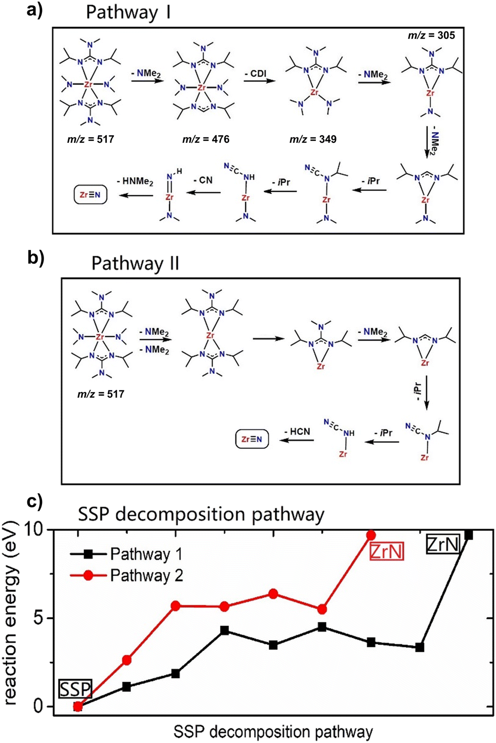
Based on experimentally obtained EI-MS fragments (Fig. S1 and Table S1†) and reported decomposition pathways of comparable guanidinate ligand containing precursors in the literature,40,41 two potential decomposition pathways (I) and (II) for the formation of ZrN from a computed 3D structure of (1) (Fig. 1) under MOCVD conditions are proposed. The schematic pathways for SSP [Zr(guan)2(NMe2)2] (1) decomposition are shown in Fig. 2(a) and (b) and the reaction energies for both pathways are shown in Fig. 2(c). They are calculated by ΔE = Epathway − ESSP + Eligand where ΔE is the computed reaction energies, Epathway, ESSP and Eligand are the energies of individual reaction steps, using the energy of the SSP as the starting point, and the energy of any ligand elimination (for example NMe2 and CDI (N,N′-diisopropylcarbodiimide)). The elimination of NMe2 fragments was studied by taking HNMe2 and H2 as references while the elimination of the CN fragment was studied by using HCN and H2 as references. The loss of NMe2 ligands from the precursor can be either NMe2 bound to CDI (pathway I) or NMe2 directly bound to Zr (pathway II). The computed energy costs for these NMe2 elimination steps are +1.12 eV for pathway I and +2.63 eV for pathway II. This difference arises from the change in Zr coordination after NMe2 elimination. In pathway I, Zr maintains its full coordination, while in pathway II, Zr coordination is lower since a Zr–N bond is removed. After the first step of NMe2 elimination, the precursor will continue losing carbodiimide (CDI) and CH3CH3CH2 (iPr) fragments. Finally, after losing another HNMe2 fragment in pathway I and a HCN fragment in pathway II, ZrN is formed using the selected precursor (1, Fig. 1). The computed overall reaction for both pathways is endothermic, indicating that the decomposition of the selected SSP will not happen at room temperature and only begins at elevated temperatures. The experimental operating temperature for optimized ZrN growth was found to be 750 °C. Overall, the intermediates calculated in pathway I possess a lower reaction energy compared to the ones in pathway II, hinting that the intermediates in I are more stable. In addition, pathway I is arguably more likely, as the precursor is forming an imido species upon decomposition, that was experimentally found in EI-MS decomposition studies of a comparable gadolinium guanidinate precursor.40,41
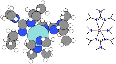 |
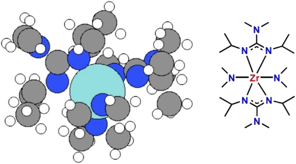
| | Fig. 1 The configuration of SSP [Zr(guan)2(NMe2)2] (1) (right) used to deposit ZrN. The left image shows a 3D structure of the precursor in which Zr is the large cyan sphere, nitrogen the blue spheres, carbon grey spheres and hydrogen white spheres. | |
 |
| | Fig. 2 The schematic for SSP decomposition mechanism: (a) pathway I, (b) pathway II, and (c) the plotted reaction energies calculated by DFT. For experimentally detected fragments, the respective m/z values are given. | |
Thin film analysis – structure and crystallinity
Optimized process parameters: substrate temperature was varied from 550 °C to 850 °C, precursor evaporation temperature was 135 °C, nitrogen carrier gas flow was 100 sccm, and the reactor pressure was 1 mbar. The influence of substrate temperature for ZrN films grown on Si and GC was investigated by means of XRD (Fig. 3(a) and (b)) as well as Raman spectroscopy (Fig. S2†) of the material on GC. The onset of crystallization was found to be 650 °C at which the (200) reflection of the rock salt ZrN phase (PDF pattern no. 00-031-1493)42 was observed. Similarly, at 750 °C, solely the (200) reflection was obtained, but with a significantly increased intensity and narrow width indicating a higher degree of crystallinity as well as a higher thickness. The XRD pattern of the film grown at 850 °C shows reflexes corresponding to the (111) and (220) plane of rock salt ZrN accompanied by a broad (200) reflection with a high intensity hinting an enhanced crystallinity but less oriented growth. Additionally, the broad peak shape indicates the presence of randomly oriented ZrN crystal domains, which could be embedded in an amorphous carbide matrix, hinted by the enhanced C content in the film as described later in Table 1. Comparison of the grain sizes estimated by the Scherrer equation43,44 confirms the temperature dependency and showcases the influence of the underlying substrate on the growth characteristics. While for the films grown on Si at 750 °C the largest grain sizes were calculated to be 25.5 nm, at 850 °C and 650 °C smaller grains with diameters of 12.4 nm and 7.4 nm were estimated, respectively. A similar trend was observed on GC, where the largest grains were obtained for the 750 °C sample with a diameter of 32.2 nm, followed by 17.9 nm for 850 °C and 10.9 nm for 650 °C. Overall, the grain sizes on GC are larger compared to those on Si at all temperatures, which could be explained by a different nucleation behaviour due to differences in surface energies leading to the formation of larger grains. The Raman spectrum of the film on GC depicted in Fig. S2† reveals three peaks corresponding to ZrN. From ∼130 cm−1 to 250 cm−1 a broad scattering peak corresponds to overlapping of the transverse acoustic phonon (TA) and the longitudinal acoustic (LA) one. In addition, the asymmetric band (2A) appears at wavenumbers around 530 cm−1. The observed Raman peaks are in accordance with literature reports for ZrN.45–47 The broad appearance of the Raman peaks indicates the presence of N vacancies in the ZrN films.46 Again, the highest intensity Raman peaks were obtained for the films grown at 750 °C, supporting the results from XRD that at this deposition temperature, films with the highest degree of crystallinity were obtained.
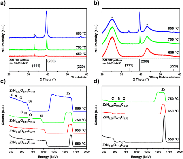 |
| | Fig. 3 (a) and (b) XRD patterns of ZrN films deposited on Si and GC respectively as a function of substrate temperature. The XRD reference pattern of ZrN from PDF pattern no. 00-031-149342 are depicted in the respective patterns. (c) and (d) RBS analysis of ZrN films grown at different temperatures on Si and GC, respectively. | |
Table 1 Composition derived from RBS/NRA measurements for ZrN thin films deposited at different temperatures
| Deposition temp. |
Zra (at%) |
Na (at%) |
Oa (at%) |
Ca (at%) |
| Si |
GC |
Si |
GC |
Si |
GC |
Si |
GC |
|
For all concentrations values an error of ±2 at% can be considered.
|
| 550 °C |
23.8 |
24.8 |
30.1 |
24.4 |
21.2 |
28.2 |
24.8 |
22.6 |
| 650 °C |
27.5 |
28.4 |
31.9 |
30.7 |
21.3 |
20.9 |
19.3 |
20.0 |
|
750 °C
|
31.1
|
29.6
|
35.7
|
35.4
|
19.0
|
19.1
|
14.3
|
16.0
|
| 850 °C |
25.2 |
— |
28.2 |
— |
10.3 |
— |
36.3 |
— |
Composition
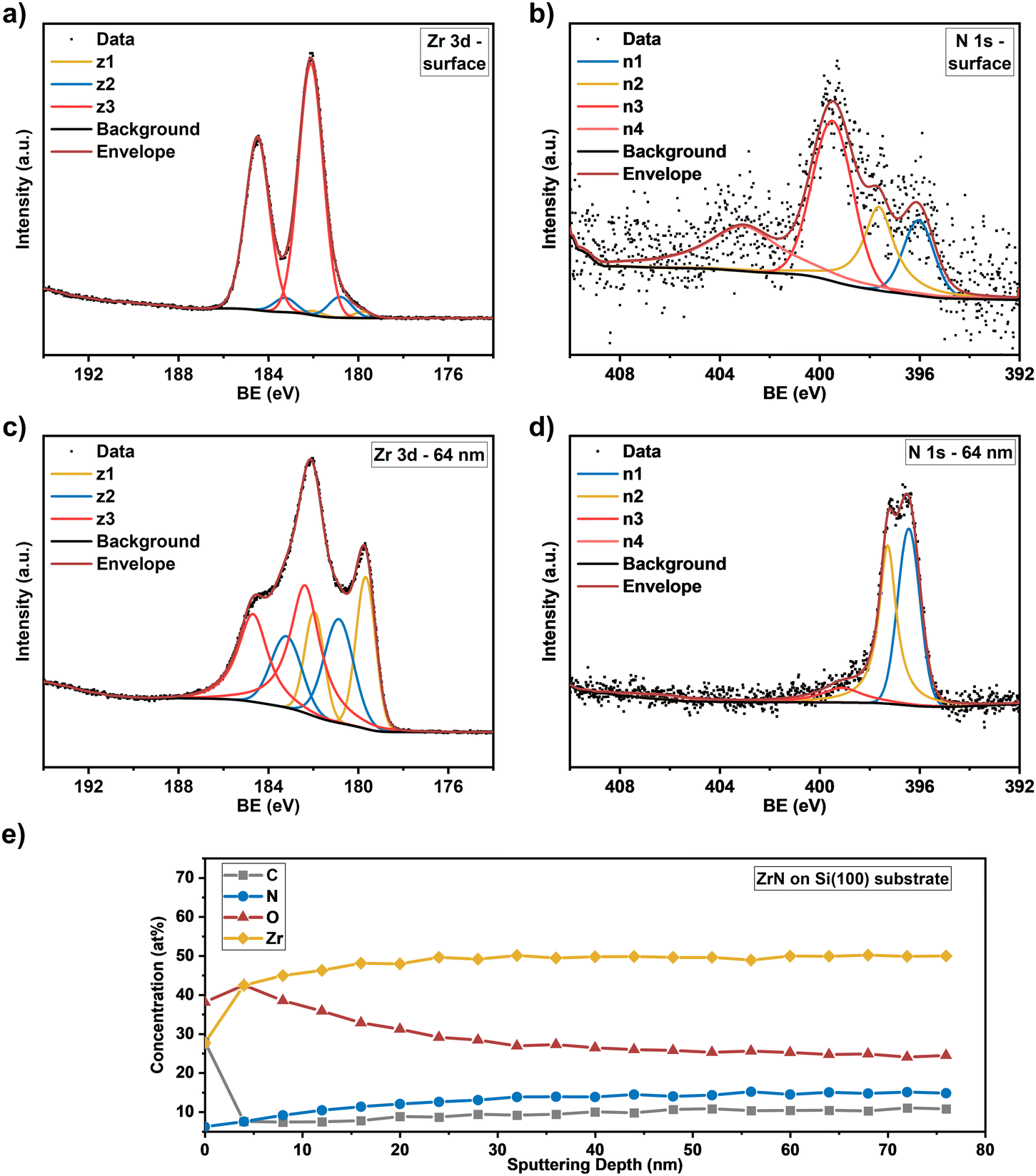
Knowing the exact composition of the ZrN material is important to investigate the influence of Zr/N ratios and impurities such as carbon and oxygen on the catalytic NRR activity. The influence of oxygen heteroatoms and the formation of oxynitrides as the active NRR phase have already been suggested for VN and CrN.48,49 The composition of the ZrN films on Si and GC was investigated by complementary analysis methods. With RBS in combination with NRA, the bulk composition of the films was determined, whereas XPS allows differentiation between Zr–N and Zr–O species on the surface as well as bulk information through depth profiling with Ar+ ion-sputtering. From RBS/NRA analysis the specific amounts of Zr, N, C and O of the films grown on Si(100) and GC were determined. These results are summarized in Table 1. At 750 °C on both Si and GC, slightly N-rich films were formed with Zr/N ratios of 0.87 and 0.84, respectively, with the lowest amount of C and O contamination. At lower deposition temperatures of 650 °C and 550 °C, the amount of C and O contamination increases significantly. The enhanced amount of C hints at an incomplete precursor reaction at lower deposition temperatures and is a known phenomenon for MOCVD processes.50 Interestingly, at 850 °C the C incorporation in the film is significantly enhanced, which was speculated from the findings in XRD analysis (Fig. 3(a) and (b)). It is most likely due to enhanced precursor decomposition at higher temperatures, where there is no sufficient time for the byproducts to leave the surface. Significant oxygen incorporation during the deposition process can be excluded because, at elevated process temperatures, crystalline ZrO2 would appear in the XRD pattern as shown by previous studies.25 More likely post-deposition oxygen incorporation occurs during sample handling under ambient conditions that is well known for ZrN and similar TMNs, which are prone to oxidation.51–53 The RBS plots in Fig. 3(c) and (d) show an increasing broadness and asymmetry of the Zr peak at higher deposition temperatures indicating a more continuous film with a higher surface roughness accompanied by a less defined interface between the film and the substrate. To investigate the nature of the different Zr species on the surface and as a function of film thickness, XPS of the surface and after Ar+-sputtering was conducted for optimized process parameters of 750 °C for Si(100) and GC substrates. Depth profiling by Ar+-sputtering (2 keV, 60 s per cycle) was performed to obtain information on the bulk composition. In total, 19 cycles were measured resulting in a depth of about 76 nm based on a sputtering rate of 4 nm min−1 determined by profilometry. Fig. 4 shows the Zr 3d and N 1s high-resolution spectra of the ZrN film on the GC substrate. The Zr 3d spectra consist of spin–orbit doublet peaks (Zr 3d5/2 and Zr 3d3/2), which were fitted with three components corresponding to different Zr species. The surface of the ZrN film is significantly oxidized apparent from the Zr 3d5/2 signal at a binding energy (BE) of 182.3 eV (ref. 53 and 54) (component z3 in Fig. 4(a)). Minor components z2 (181.2 eV) and z1 (180.0 eV) can be allocated to the oxynitride and nitride species,53 respectively, indicating a contribution from the underlying ZrN phase below the oxidized surface. Thus, the XPS sampling depth of 10 nm (ref. 55) is greater than the thickness of the surface oxide layer, which was described in the literature to be around 3.7 nm.53 The oxynitride can be present as a particular phase but was also described as an interfacial layer between the oxide and nitride layers for different TMNs.56
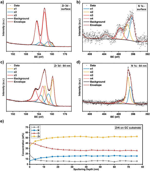 |
| | Fig. 4 High resolution core level spectra of (a) Zr 3d at the surface and (c) at a sputtering depth of 64 nm and (b) N 1s at the surface and (d) at a sputtering depth of 64 nm for the ZrN film. (e) Concentration profile of the elements (Zr, N, O, C) as a function of sputtering depth on the GC substrate. | |
The Zr 3d spectra of the ZrN film deposited on Si substrates (Fig. 5(a)) are very similar, however, the component z1 (179.8 eV) assigned as the ZrN phase is smaller, indicating a thicker surface oxide layer. Components z2 (180.8 eV) and z3 (182.1 eV) occurred at similar BE values than for the film on the GC substrate. The Zr 3d spectra correspond to the surface N 1s and O 1s spectra. In the case of the ZrN-GC sample, four nitrogen components were identified (Fig. 4(b)) with n1 at 396.2 eV being dominant and corresponding to the oxynitride phase. Component n2 (397.6 eV) is assigned as the nitride phase and component n3 (399.6 eV) as adsorbed nitrogen.53,54 The component n4 (403.5 eV) was either assigned as molecular N2 (ref. 57) or oxidized nitrogen species.56 The high-resolution N 1s spectra of the ZrN–Si sample (Fig. 5(b)) show similar components, but lower contributions of n1 and n2 in comparison to n3 supporting the hypothesis of a thicker oxide layer as discussed for the Zr 3d spectra. Due to the possible surface oxidation of TMNs when exposed to the ambient atmosphere, XPS analysis of nitrides is often performed on a sputter-cleaned surface. Moreover, XPS depth profiling by sputtering with Ar+-ions (also applied here) enables analysis of the film's bulk composition. However, sputtering also introduces uncertainties to the analysis due to various effects such as preferential sputtering of one element in a multielement sample that could result in the variation in the atomic concentration or cascade mixing where smearing of one element results in the appearance of this element in deeper levels than in the pristine sample.53,58 This complexity has to be considered in the evaluation of the XPS depth profiling. Here, Ar+-sputtering (2 keV, 60 s, 19 cycles) was performed to analyse the bulk composition of the ZrN films, which resulted in a total depth of 76 nm. High-resolution spectra after 16 cycles (64 nm depth) are compared to the surface spectra. Zr 3d spectra of the ZrN-GC sample (Fig. 4(c)) show increased nitride (z1, 179.7 eV) and oxynitride (z2, 181.0 eV) components, but still a large contribution of the oxide phase (z3, 182.7 eV) is present. Thus, surface oxides are smeared from the surface to the bulk due to sputtering or oxides are formed from containing oxygen in the pristine film as determined by RBS/NRA (Table 1). Because no oxide phase is visible in XRD measurements, observed oxide components are of an amorphous nature from oxidation under ambient conditions. For the ZrN-Si(100) sample, a similar behavior is visible with an even higher contribution of the oxide phase in comparison to the nitride component (Fig. 5(c)). Again, high-resolution N 1s spectra correspond to these observations with increasing components of nitride (n2) and oxynitride (n1) (Fig. 5(d)). The bulk composition was studied by analysing the atomic concentration of Zr, N, O and C dependent on the sputtering depth. For the ZrN-GC sample (Fig. 4(e)) the surface contains 40 at% O, 35 at% Zr, 18 at% C and only 7 at% N. The amount of C decreases fast to a value of 6–7 at% after removing adventitious carbon in the first layer, while the amount of O gradually decreases and the amount of N and Zr gradually increases. The bulk composition of 52 at% Zr, 26 at% O and 16 at% N shows a stronger oxygen content as expected and is visible in RBS/NRA analysis. Possible reasons could be the smearing effect of O from the surface to the bulk during sputtering53 and the preferential sputtering of N compared to Zr resulting in N-deficient compositions.58 The ZrN-Si(100) sample (Fig. 5(e)) shows again a very similar trend with slightly different numbers. In summary, XPS analysis clearly shows the surface oxidation of ZrN films but also the large contributions of oxide phases in the bulk after sputtering. The higher values of oxygen content in comparison to RBS/NRA analysis could be a reason for the sputtering process itself, which results in uncertainties in the determination of the elemental composition.
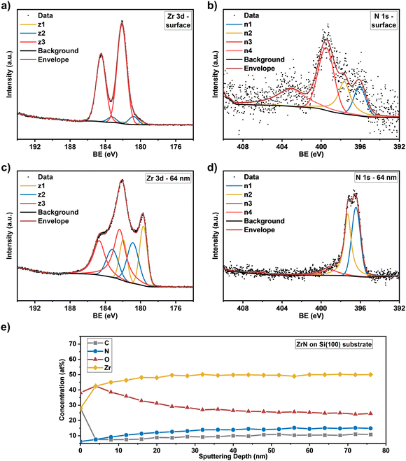 |
| | Fig. 5 High resolution core level spectra of (a) Zr 3d at the surface and (c) at a sputtering depth of 64 nm and (b) N1s at the surface and (d) at a sputtering depth of 64 nm for the ZrN film. (e) Concentration profile of the elements (Zr, N, O, C) as a function of sputtering depth on the Si(100) substrate. | |
To study the oxidation of ZrN thin film under ambient oxygen conditions, ab initio molecular dynamics (aiMD) calculations were performed on a ZrN(100) surface at room temperature in the NVT (canonical) ensemble with VASP 5.4. The ZrN substrate is represented by a (3 × 3) surface supercell, with a thickness of four layers. The unit cell of ZrN has a computed lattice constant of a = b = c = 3.26 Å and angles of α = β = γ = 60°. We added 8 oxygen atoms (4 O2 dissociated molecules) above the ZrN(100) surface at random locations in each aiMD calculation. The time step was 2.5 fs with a total running time of 6.25 ps. In total, we performed three rounds of aiMD calculations, and the resulting structure (side view and top view) is shown in Fig. 6, with the final surface termination containing 8 oxygen atoms at the surface (ZrO8/ZrN). A movie of an aiMD simulation is shown in the ESI.† We found that at room temperature, the O atoms react rapidly at ZrN, displacing Zr species outwards to form new Zr–O bonds (with typical Zr–O distances of 1.91 Å to 2.2 Å) and N atoms are pushed into the first subsurface layer. This yields a surface termination of ZrO8/ZrN, with oxygen exclusively located at the surface of the ZrN surface and not undergoing migration into bulk at this temperature. Surface oxygen heteroatoms neighbouring N vacancies are discussed to influence the mechanistic steps of the Mars-van-Krevelen mechanism, thus forming the active phase for the NRR, which has already been suggested for oxynitrides of VN and CrN.48,49 A more detailed study of the role of oxygen functionalities in ZrN films will be presented in later work but this result is shown to demonstrate the ease with which ambient oxidation can oxidize the surface layer of ZrN to produce a ZrOxNy film. This is perfectly in line with the experimental composition results and concentration analysis with the sputtering depth.
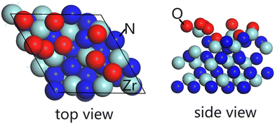 |
| | Fig. 6 The configuration of the structure after the MD calculation on ZrN(100) surface in ambient oxygen condition at room temperature. Left: top view, right: side view. | |
Morphology
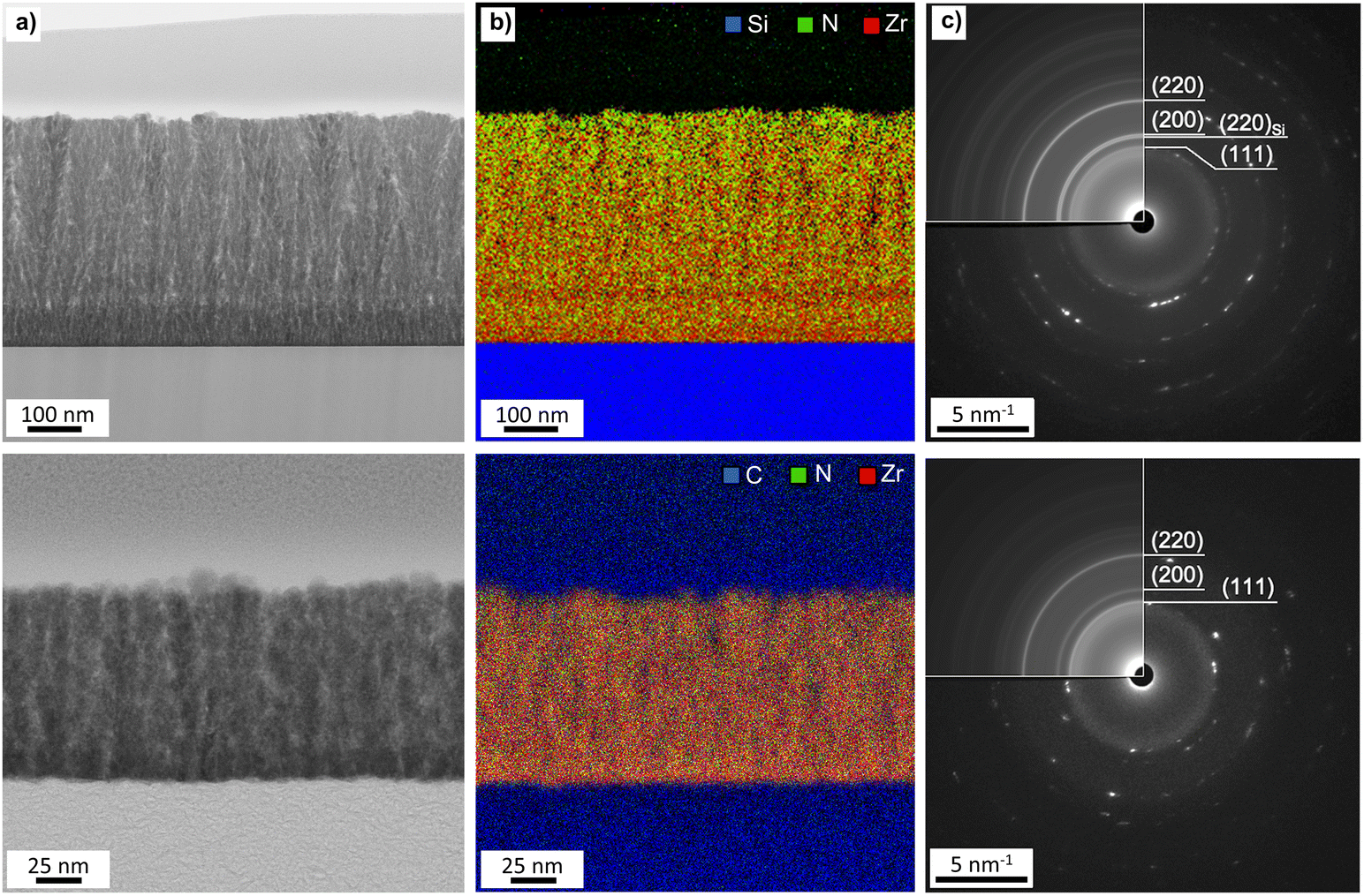
Further insight into the morphology of the thin films was obtained by SEM analysis. The SEM images in Fig. 7 depict the impact of the deposition temperature on the structure of the ZrN crystallites. At 750 °C, distinct cauliflower-shaped crystallites with diameters between 25 nm and 75 nm were obtained. While the shape of the crystallites is comparable at 650 °C, the size of the crystallites is decreasing to 25 nm–50 nm. At 850 °C, the crystallites merge, and less oriented agglomerates ranging from 50 nm to 450 nm are formed. This correlates with the loss of facet-favoured growth at this temperature observed in the XRD pattern (Fig. 3(a) and (b)). From cross-section SEM images (inset of Fig. 7, middle) of the 750 °C samples, oriented columnar growth is apparent on both substrates and thicknesses of 330 nm and 370 nm on Si and GC were estimated, respectively. To further investigate the films in terms of crystallite shape, element distribution and crystal structure, BF-TEM, STEM-EDS and SAED analysis were conducted on ZrN films grown at 750 °C on Si and GC. Cross-sectional BF-TEM images (Fig. 8(a)) reveal the columnar growth of the thin films on both substrates. Interestingly, the initial film growth on Si leads to a film of higher density compared to the rest of the sample, as it is significantly darker compared to the rest of the film. The STEM-EDS of the film on Si (Fig. 8(b)) reveals varying N concentrations throughout the film. At the substrate/film interface, Zr (red) and N (green) signals are evenly distributed, whereas close to the nitride surface, the amount of N is significantly increased. Simultaneously, the density of the film is decreasing in the N-rich regime. Noteworthily, STEM-EDS on GC reveals a more even distribution of Zr and N throughout the whole film (Fig. 8(b)). This can be explained by the difference in film thicknesses, as the film on Si is four times thicker compared to the one on GC. The decreasing Zr/N ratio, as well as the initial film growth with higher density, can be attributed to substrate-dependent growth, particularly in the initial film deposition stage. After the initial growth, the ZrN formation is preferred on the existing crystallites which facilitate the columnar growth. Furthermore, the rather porous structure of the films allows a post-deposition oxidation beyond the surface and could explain the significant oxygen content in the bulk of the films. SAED of the films on both substrates was carried out revealing distinct diffraction spots along the circles corresponding to cubic ZrN further confirming the growth of crystalline ZrN.
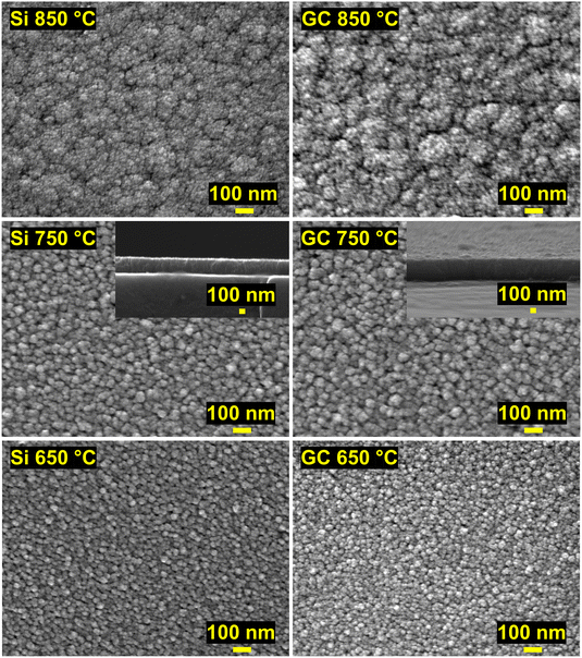 |
| | Fig. 7 Top view SEM images of ZrN on Si (left) and GC (right) deposited at 850 °C (top), 750 °C (middle) and 650 °C (bottom). Cross section images of the film deposited at 750 °C are shown in the inset. | |
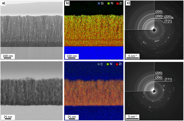 |
| | Fig. 8 (a) BF-TEM, (b) STEM-EDS and (c) SAED of ZrN deposited at 750 °C on Si (top) and GC (bottom). Rotational averaging (inserts) is used in the identification of both diffracted planes. The patterns are indexed as ZrN using inorganic crystal structures data from ICSD-131632 (ICSD release 2021 02 01).38,39 | |
Functional properties
Optical properties.
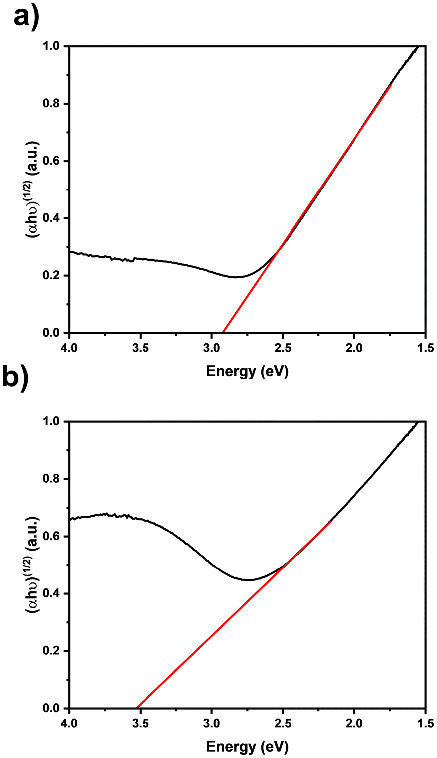
To investigate the optical properties of the ZrN films, Tauc plots59 were derived from diffuse UV-vis reflection measurements of films with varying thicknesses (Fig. 9). The thicker sample (Fig. 9(a)) exhibits a smaller band gap energy of 2.91 eV compared to the thinner one (Fig. 9(b)) with an energy of 3.50 eV. In both cases, the determined values deviate from the reported literature range for ZrN, which is typically between 2.6 to 2.8 eV.60–62 It is known that zirconium oxynitrides, which are formed after the deposition due to the contact with ambient atmosphere, tend to have larger band gaps with increasing oxygen content.63 The disparities observed in these samples can be attributed to the known presence of oxygen and carbon (Table 1) and suggest a self-limited and therefore thickness thickness-dependent oxidation of the ZrN film, as the thicker sample has a lower relative ZrOxNy component and therefore a lower band gap energy. Both samples manifest a band gap situated in the transitional range between visible and ultraviolet light.
 |
| | Fig. 9 Tauc plots of ZrN films on quartz glass deposited for (a) 30 min and (b) 10 min. | |
Electrochemical characterization.
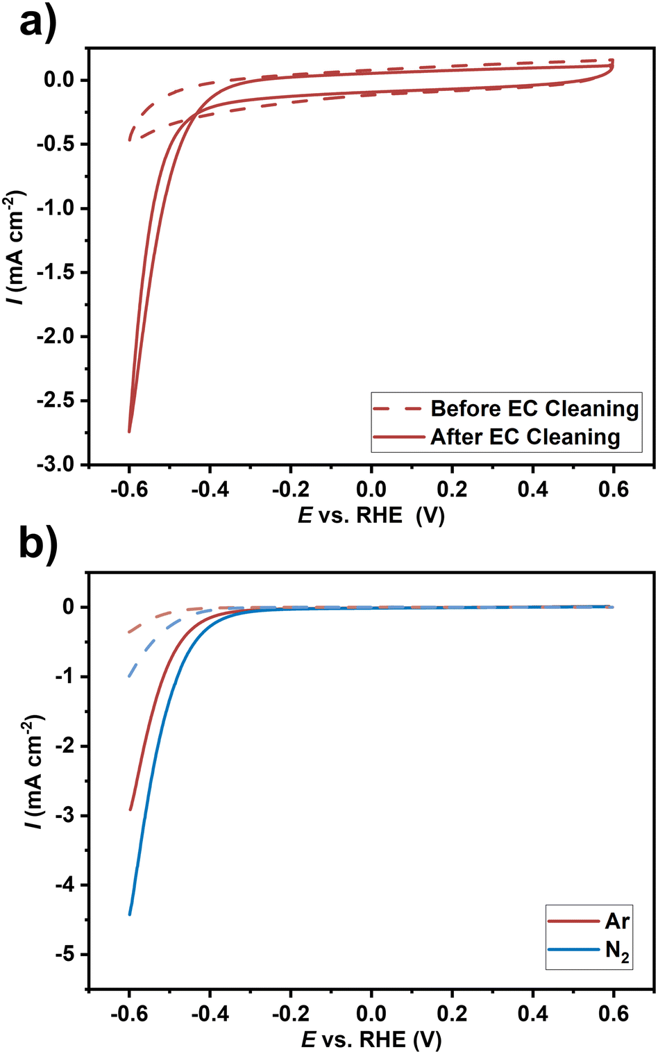
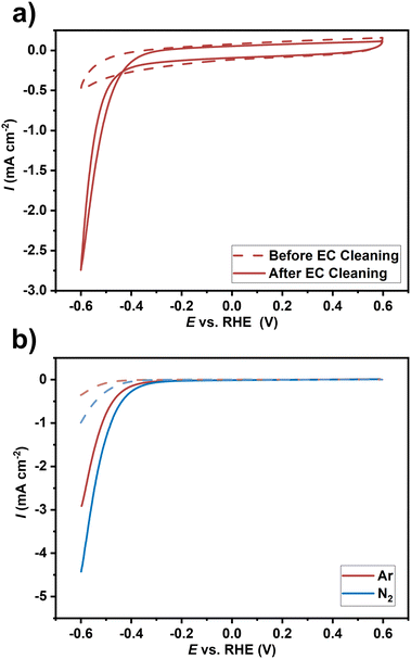
Optimized ZrN film on GC substrate deposited at a temperature of 750 °C was subjected to a basic electrochemical evaluation to study the potential application of the developed catalyst films for the NRR in regards to stability in the respective NRR potential window and the current propagation in electrodynamic measurements. These measurements give only a qualitative hint of potential activity for the NRR and do not prove genuine NRR activity, which will be investigated in our future work. First, electrochemical characterization was performed in an Ar-saturated 0.1 M sulphuric acid electrolyte. The upper potential limit was limited in all experiments to 0.6 V (approximately the initial value of open circuit potential) to avoid any catalyst oxidation. As the ZrN material is prone to surface oxidation, the surface oxide layer was purposely removed by electrochemical (EC) cleaning as suggested in the literature32 using cyclic voltammetry (CV) with 250 mV s−1 for 25 scans. CV before and after EC cleaning was applied to evaluate changes due to electrochemical treatment (Fig. 10(a)). The current in CV measurements after EC cleaning is apparently higher (more negative). This can be explained by an activation process for the ongoing HER at these potentials possibly due to the removal of the oxide layer. Comparison of the CV data in Ar- and N2-saturated electrolytes (Fig. 10(b)) showed higher currents for the latter case, which could result from the NRR reaction in addition to the HER. In general, the selectivity in regard to the competitive HER is a challenge in NRR research where several strategies are discussed.64 However, the magnitude of the difference of the currents here is rather high compared to other qualitative electrochemical investigations. The onset potential decreases and the maximum current increases from roughly −3 to −4.5 mA cm−2 at the lower potential limit of −0.6 V. This difference could qualitatively hint towards a possible activity for the electrochemical NRR of the ZrN film. Similarly, Hanifpour et al.32 observed a similar current increase for polycrystalline ZrN films and also for other TMNs.65–67 Although it is compelling to attribute this difference to the NRR, this is only a qualitative indication. Proving genuine NRR activity, which is beyond the scope of this study, would require confirmation of ammonia formation.68 Robust electrochemical protocols have to be followed including 15N2-labelled isotope experiments to avoid false positive results due to contaminations and other effects.69,70 Moreover, TMN is also discussed to undergo non-catalytic decomposition resulting in ammonia formation instead of genuine NRR.68 Thus, there is currently not a conclusive picture of the real NRR activity of TMNs, although they have theoretically described promising catalytic potential for the NRR via the Mars-van Krevelen mechanism.71 We believe the synthetic capabilities of the presented faceted ZrN growth and qualitative electrochemical investigations in this study in conjunction with prospective further quantitative electrochemical investigation necessary in NRR research could help to shed light on the real NRR potential of TMNs.
 |
| | Fig. 10 Electrochemical characterization of the ZrN-GC sample in 0.1 M sulfuric acid electrolyte with (a) showing the cyclic voltammetry data before (dashed line) and after (solid line) electrochemical cleaning and (b) the difference in cyclic voltammetry (10 mV s−1) in Ar- (red) and N2 (blue)-saturated electrolyte. Shown is the backward scan of the 3rd scan. Dashed lines indicate background measurements of the glassy carbon substrate. | |
Conclusions
Taking ZrN as a model catalyst for NRR, we optimized the MOCVD route to grow oriented crystalline ZrN layers with facetted growth along the (100) plane on Si and GC substrates, which were described as theoretically active for the NRR. This is the first case study where a CVD-grown oriented ZrN material system has been investigated from a point of view of potentially using it for NRR. The specific choice of the Zr precursor comprising a preformed Zr–N bond enables the controlled growth of ZrN. This was proved experimentally and theoretically where the SSP decomposition reaction pathway towards nitride thin films was elucidated. Compositional analysis revealed slightly nitrogen-rich films with a certain amount of oxygen incorporation. XPS sputtering study indicates post-deposition oxidation, predominantly on the surface, which is also demonstrated by an aiMD calculation of a model ZrN(100) surface reacting with O atoms under ambient conditions yielding a surface termination of ZrO8/ZrN. SEM reveals a high surface area of the films and cross-sectional BF-TEM illustrated a columnar growth on both substrates. Furthermore, STEM-EDS and SAED reveal a varying distribution of Zr and N throughout the film as well as crystalline rock salt ZrN, respectively. Band gap energies were found to be thickness-dependent, which increased with a decrease in the thickness. This suggests self-limiting surface oxidation of the ZrN films under ambient conditions since a thinner film has a relatively larger ZrOxNy region. Qualitative electrochemical CV experiments of the ZrN films on GC in Ar- and N2-saturated electrolytes revealed a higher current in the latter electrolyte, suggesting potential NRR activity of ZrN. Although more detailed studies are required to prove genuine NRR activity, the ability to fabricate potentially NRR active catalyst materials via MOCVD forms the basis to tailor the surface towards optimized activity. Our future work will focus on benchmarking the oriented ZrN model studied here and extending it to other TMNs. Attempts to prevent post-oxidation and the role of substrates will be the aspects that will be investigated in our follow-up study.
Author contributions
JPG: conceptualization, precursor synthesis, MOCVD process development and film characterization, methodology, data curation, and major manuscript writing. JL: XPS, electrochemical analysis, methodology, funding acquisition. J. Liu: DFT studies, methodology. BM: UV-vis, data acquisition and analysis. SB: funding acquisition and data curation. AK: TEM data acquisition and analysis. DR: RBS/NRA data acquisition and analysis. MW: conceptualization and funding acquisition. CH: funding acquisition. AD: conceptualization, funding acquisition and project administration. All authors contributed to the manuscript and have given approval to the final version of the manuscript.
Conflicts of interest
There are no conflicts to declare.
Data availability
The data supporting this article have been included as part of the ESI.†
Acknowledgements
This work was funded by the German Research Foundation (Deutsche Forschungsgemeinschaft, DFG, project number 502054395) within the priority program SPP 2370. J. Liu would acknowledge the support from HPC Vega in Slovenia through EuroHPC JU call project. The XPS device is funded by the German Research Foundation (DFG) through grant INST 184/144-1 FUGG.
References
- H. Wang, J. Li, K. Li, Y. Lin, J. Chen, L. Gao, V. Nicolosi, X. Xiao and J.-M. Lee, Chem. Soc. Rev., 2021, 50, 1354–1390 RSC.
- W. Bi, Z. Hu, X. Li, C. Wu, J. Wu, Y. Wu and Y. Xie, Nano Res., 2015, 8, 193–200 CrossRef CAS.
- B. Gao, X. Li, K. Ding, C. Huang, Q. Li, P. K. Chu and K. Huo, J. Mater. Chem. A, 2019, 7, 14–37 RSC.
-
H. O. Pierson, Handbook of refractory carbides and nitrides. Properties, characteristics, processing, and applications, Noyes Publ, Westwood, NJ, 1996 Search PubMed.
- K. Schwarz, Crit. Rev. Solid State Mater. Sci., 1987, 13, 211–257 CrossRef CAS.
- X. Peng, C. Pi, X. Zhang, S. Li, K. Huo and P. K. Chu, Sustainable Energy Fuels, 2019, 3, 366–381 RSC.
-
W. Lengauer, in Handbook of Ceramic Hard Materials, ed. R. Riedel, Wiley-VCH Verlag GmbH, Weinheim, Germany, 2000, pp. 202–252 Search PubMed.
- D. Ham and J. Lee, Energies, 2009, 2, 873–899 CrossRef CAS.
- A. Shabani, M. T. Korsa, S. Petersen, M. K. Nezhad, Y. K. Mishra and J. Adam, Adv. Photonics Res., 2021, 2, 2100178 CrossRef CAS.
- Y. Yuan, J. Wang, S. Adimi, H. Shen, T. Thomas, R. Ma, J. P. Attfield and M. Yang, Nat. Mater., 2020, 19, 282–286 CrossRef CAS PubMed.
- Y. Abghoui, A. L. Garden, J. G. Howalt, T. Vegge and E. Skúlason, ACS Catal., 2016, 6, 635–646 CrossRef CAS.
- J. Xie and Y. Xie, Chem. – Eur. J., 2016, 22, 3588–3598 CrossRef CAS PubMed.
- N. Sucheewa, W. Wongwiriyapan, P. Rattanawarinchai, T. Wuttikhun, K. Sinthiptharakoon, S. Youngjan, P. Khemthong, G. Tumcharern, T. Lertvanithphol, N. Limsuwan, A. Pankiew, M. Horprathum, S. Porntheeraphat, V. Yordsri, N. Khemasiri, M. Obata, M. Fujishige, K. Takeuchi, M. Endo, A. Klamchuen and J. Nukeaw, Adv. Mater. Interfaces, 2023, 10, 2300472 CrossRef CAS.
- M. M. Larijani, M. Kiani, M. Tanhayi and A. Majdabadi, Cryst. Res. Technol., 2011, 46, 351–356 CrossRef CAS.
- L. Mirenghi and A. Rizzo, Appl. Sci., 2023, 13, 1271 CrossRef CAS.
- H. Yanagisawa, S. Shinkai, K. Sasaki, Y. Abe, A. Sakai and S. Zaima, Jpn. J. Appl. Phys., 2005, 44, 343 CrossRef CAS.
- Y. Aihara, T. Iida, K. Kodama, H. Iwata and T. Sekiya, J. Vac. Sci. Technol., B, 2024, 42, 034202 CrossRef CAS.
- W. S. Rees, Adv. Mater., 1995, 7, 96 CrossRef.
-
H. O. Pierson, Handbook of chemical vapor deposition (CVD). Principles, technology, and applications, Noyes Publ, Norwich, NY, 2nd edn, 1999 Search PubMed.
- A. Schlegel, P. Wachter, J. J. Nickl and H. Lingg, J. Phys. C: Solid State Phys., 1977, 10, 4889–4896 CrossRef CAS.
- B. Karlsson, R. P. Shimshock, B. O. Seraphin and J. C. Haygarth, Sol. Energy Mater., 1983, 7, 401–411 CrossRef CAS.
- A. Yajima, Y. Segawa, R. Matsuzaki and Y. Saeki, Bull. Chem. Soc. Jpn., 1983, 56, 2638–2642 CrossRef CAS.
- H. Wendel and H. Suhr, Appl. Phys. A, 1992, 54, 389–392 CrossRef.
- B. W. Lamm and D. J. Mitchell, Coatings, 2023, 13, 266 CrossRef CAS.
- M. Banerjee, N. B. Srinivasan, H. Zhu, S. J. Kim, K. Xu, M. Winter, H.-W. Becker, D. Rogalla, T. de los Arcos, D. Bekermann, D. Barreca, R. A. Fischer and A. Devi, Cryst. Growth Des., 2012, 12, 5079–5089 CrossRef CAS.
- Q. Luo, C. Lu, L. Liu and M. Zhu, Green Energy Environ., 2023, 8, 406–437 CrossRef CAS.
- Y. Abghoui, A. L. Garden, V. F. Hlynsson, S. Björgvinsdóttir, H. Ólafsdóttir and E. Skúlason, Phys. Chem. Chem. Phys., 2015, 17, 4909–4918 RSC.
- Y. Abghoui and E. Skúlason, Catal. Today, 2017, 286, 69–77 CrossRef CAS.
- D. Guo, S. Wang, J. Xu, W. Zheng and D. Wang, J. Energy Chem., 2022, 65, 448–468 CrossRef CAS.
- Z. Qiao, D. Johnson and A. Djire, Cell Rep. Phys. Sci., 2021, 2, 100438 CrossRef CAS.
- E. Skúlason, T. Bligaard, S. Gudmundsdóttir, F. Studt, J. Rossmeisl, F. Abild-Pedersen, T. Vegge, H. Jónsson and J. K. Nørskov, Phys. Chem. Chem. Phys., 2012, 14, 1235–1245 RSC.
- F. Hanifpour, C. P. Canales, E. G. Fridriksson, A. Sveinbjörnsson, T. K. Tryggvason, J. Yang, C. Arthur, S. Jónsdóttir, A. L. Garden, S. Ólafsson, K. Leósson, L. Árnadóttir, E. Lewin, Y. Abghoui, Á. S. Ingason, F. Magnus, H. D. Flosadóttir and E. Skúlason, J. Catal., 2022, 413, 956–967 CrossRef CAS.
- S. Z. Andersen, V. Čolić, S. Yang, J. A. Schwalbe, A. C. Nielander, J. M. McEnaney, K. Enemark-Rasmussen, J. G. Baker, A. R. Singh, B. A. Rohr, M. J. Statt, S. J. Blair, S. Mezzavilla, J. Kibsgaard, P. C. K. Vesborg, M. Cargnello, S. F. Bent, T. F. Jaramillo, I. E. L. Stephens, J. K. Nørskov and I. Chorkendorff, Nature, 2019, 570, 504–508 CrossRef CAS PubMed.
- G. Kresse and D. Joubert, Phys. Rev. B: Condens. Matter Mater. Phys., 1999, 59, 1758–1775 CrossRef CAS.
- J. P. Perdew, J. A. Chevary, S. H. Vosko, K. A. Jackson, M. R. Pederson, D. J. Singh and C. Fiolhais, Phys. Rev. B: Condens. Matter Mater. Phys., 1992, 46, 6671–6687 CrossRef CAS PubMed.
- J. P. Perdew, K. Burke and M. Ernzerhof, Phys. Rev. Lett., 1996, 77, 3865–3868 CrossRef CAS PubMed.
-
M. Mayer, SIMNRA User's Guide, Report IPP 9/113, Max-Planck-Institut für Plasmaphysik, Garching, Germany, 1997 Search PubMed.
- D. Zagorac, H. Müller, S. Ruehl, J. Zagorac and S. Rehme, J. Appl. Crystallogr., 2019, 52, 918–925 CrossRef CAS PubMed.
- M. Yang, J. A. Rodgers, L. C. Middler, J. Oró-Solé, A. B. Jorge, A. Fuertes and J. P. Attfield, Inorg. Chem., 2009, 48, 11498–11500 CrossRef CAS PubMed.
- A. Devi, Coord. Chem. Rev., 2013, 257, 3332–3384 CrossRef CAS.
- A. P. Milanov, T. B. Thiede, A. Devi and R. A. Fischer, J. Am. Chem. Soc., 2009, 131, 17062–17063 CrossRef CAS PubMed.
- A. N. Christensen, Acta Chem. Scand., 1975, 29a, 563 CrossRef.
-
Chemische Technologie in Einzeldarstellungen, ed. P. Scherrer, Springer Berlin Heidelberg, Berlin, Heidelberg, 1912 Search PubMed.
- J. I. Langford and A. J. C. Wilson, J. Appl. Crystallogr., 1978, 11, 102–113 CrossRef CAS.
- A. Singh, P. Kuppusami, S. Khan, C. Sudha, R. Thirumurugesan, R. Ramaseshan, R. Divakar, E. Mohandas and S. Dash, Appl. Surf. Sci., 2013, 280, 117–123 CrossRef CAS.
- Q. Chen, S. Yang, C. Li, W. Yao, X. Liu, H. Niu, R. Yang, H. Li, H. Wei, L. Wang and Z. Wang, J. Phys. D: Appl. Phys., 2022, 55, 404003 CrossRef CAS.
- C. Moura, P. Carvalho, F. Vaz, L. Cunha and E. Alves, Thin Solid Films, 2006, 515, 1132–1137 CrossRef CAS.
- X. Yang, J. Nash, J. Anibal, M. Dunwell, S. Kattel, E. Stavitski, K. Attenkofer, J. G. Chen, Y. Yan and B. Xu, J. Am. Chem. Soc., 2018, 140, 13387–13391 CrossRef CAS PubMed.
- Y. Yao, Q. Feng, S. Zhu, J. Li, Y. Yao, Y. Wang, Q. Wang, M. Gu, H. Wang, H. Li, X.-Z. Yuan and M. Shao, Small Methods, 2019, 3, 1800324 CrossRef.
- S. M. Beer, D. Samelor, A. A. Aal, J. Etzkorn, D. Rogalla, A. E. Turgambaeva, J. Esvan, A. Kostka, C. Vahlas and A. Devi, J. Mater. Res. Technol., 2021, 13, 1599–1614 CrossRef CAS.
- M. Ritala, M. Leskelä, E. Rauhala and P. Haussalo, J. Electrochem. Soc., 1995, 142, 2731–2737 CrossRef CAS.
- H. Kim, A. J. Kellock and S. M. Rossnagel, J. Appl. Phys., 2002, 92, 7080–7085 CrossRef CAS.
- T. Muneshwar and K. Cadien, Appl. Surf. Sci., 2018, 435, 367–376 CrossRef CAS.
- M. Matsuoka, S. Isotani, W. Sucasaire, N. Kuratani and K. Ogata, Surf. Coat. Technol., 2008, 202, 3129–3135 CrossRef CAS.
- F. A. Stevie and C. L. Donley, J. Vac. Sci. Technol., A, 2020, 38, 063204 CrossRef CAS.
- R. Zeng, Y. Yang, X. Feng, H. Li, L. M. Gibbs, F. J. DiSalvo and H. D. Abruña, Sci. Adv., 2022, 8, eabj1584 CrossRef CAS PubMed.
- I. Milošev, H.-H. Strehblow, M. Gaberšček and B. Navinšek, Surf. Interface Anal., 1996, 24, 448–458 CrossRef.
- G. Greczynski, D. Primetzhofer, J. Lu and L. Hultman, Appl. Surf. Sci., 2017, 396, 347–358 CrossRef CAS.
- J. B. Coulter and D. P. Birnie, Phys. Status Solidi B, 2018, 255, 1700393 CrossRef.
- H.-D. Kim, H.-M. An, K. H. Kim, S. J. Kim, C. S. Kim, J. Cho, E. F. Schubert and T. G. Kim, Adv. Funct. Mater., 2014, 24, 1575–1581 CrossRef CAS.
- A. W. Amer, M. A. El-Sayed and N. K. Allam, J. Phys. Chem. C, 2016, 120, 7025–7032 CrossRef CAS.
- A. W. Amer, S. M. Mohamed, A. M. Hafez, S. Y. AlQaradawi, A. S. Aljaber and N. K. Allam, RSC Adv., 2014, 4, 36336–36343 RSC.
- M. Laurikaitis, S. Burinskas, J. Dudonis and D. Milčius, J. Phys.: Conf. Ser., 2008, 100, 82051 CrossRef.
- A. R. Singh, B. A. Rohr, J. A. Schwalbe, M. Cargnello, K. Chan, T. F. Jaramillo, I. Chorkendorff and J. K. Nørskov, ACS Catal., 2017, 7, 706–709 CrossRef CAS.
- L. Zhang, X. Ji, X. Ren, Y. Luo, X. Shi, A. M. Asiri, B. Zheng and X. Sun, ACS Sustainable Chem. Eng., 2018, 6, 9550–9554 CrossRef CAS.
- F. Hanifpour, C. P. Canales, E. G. Fridriksson, A. Sveinbjörnsson, T. K. Tryggvason, E. Lewin, F. Magnus, Á. S. Ingason, E. Skúlason and H. D. Flosadóttir, Electrochim. Acta, 2022, 403, 139551 CrossRef CAS.
- R. Zhang, Y. Zhang, X. Ren, G. Cui, A. M. Asiri, B. Zheng and X. Sun, ACS Sustainable Chem. Eng., 2018, 6, 9545–9549 CrossRef CAS.
- H.-L. Du, T. R. Gengenbach, R. Hodgetts, D. R. MacFarlane and A. N. Simonov, ACS Sustainable Chem. Eng., 2019, 7, 6839–6850 CrossRef CAS.
- H. Iriawan, S. Z. Andersen, X. Zhang, B. M. Comer, J. Barrio, P. Chen, A. J. Medford, I. E. L. Stephens, I. Chorkendorff and Y. Shao-Horn, Nat. Rev. Methods Primers, 2021, 1, 56 CrossRef CAS.
- J. Choi, B. H. R. Suryanto, D. Wang, H.-L. Du, R. Y. Hodgetts, F. M. Ferrero Vallana, D. R. MacFarlane and A. N. Simonov, Nat. Commun., 2020, 11, 5546 CrossRef CAS PubMed.
- Z. Qiao, D. Johnson and A. Djire, Cell Rep. Phys. Sci., 2021, 2, 100438 CrossRef CAS.
|
| This journal is © The Royal Society of Chemistry 2024 |
Click here to see how this site uses Cookies. View our privacy policy here. 
 Open Access Article
 This Open Access Article is licensed under a
  a,
Julian
Lorenz
a,
Julian
Lorenz