Multilayer stacked ultra-wideband perfect solar absorber and thermal emitter based on SiO2-InAs-TiN nanofilm structure
Peng
Chen
a,
Qianju
Song
 a,
Can
Ma
b,
Zao
Yi
 *abc,
Liang
Bian
a,
Shubo
Cheng
d,
Zhiqiang
Hao
e,
Tangyou
Sun
f,
Pinghui
Wu
 g and
Qingdong
Zeng
h
aSchool of Mathematics and Science, Joint Laboratory for Extreme Conditions Matter Properties, The State Key Laboratory of Environment-friendly Energy Materials, Tianfu Institute of Research and Innovation, Southwest University of Science and Technology, Mianyang 621010, China. E-mail: yizaomy@swust.edu.cn
bDepartment of Oncology, Sichuan Science City Hospital, Mianyang, Sichuan Province 621000, China
cSchool of Chemistry and Chemical Engineering, Jishou University, Jishou 416000, China
dSchool of Physics and Optoelectronic Engineering, Yangtze University, Jingzhou, Hubei 434023, China
eHubei Key Laboratory of Mechanical Transmission and Manufacturing Engineering, Wuhan University of science and Technology, Wuhan 430081, China
fGuangxi Key Laboratory of Precision Navigation Technology and Application, Guilin University of Electronic Technology, Guilin 541004, China
gCollege of Physics & Information Engineering, Quanzhou Normal University, Quanzhou 362000, China
hSchool of Physics and Electronic-information Engineering, Hubei Engineering University, Xiaogan 432000, China
First published on 2nd July 2024
Abstract
In this paper, a broadband solar absorber is constructed and simulated based on the finite difference time domain method (FDTD). The modeled structure of the absorber consists of cyclic stacking of five absorber cells with different periods on refractory metal W, where a single absorber cell is composed of a three-layer SiO2-InAs-TiN square film. Due to the Fabry–Perot resonance and the surface plasmon resonance (SPR), an absorptivity greater than 90% within a bandwidth of 2599.5 nm was achieved for the absorber. Notably, one of these bands, 2001 nm, is a high-efficiency absorption with an absorption rate greater than 99%. The average absorption efficiency reaches 99.31% at an air mass of 1.5 (AM 1.5), and the thermal radiation efficiencies are 97.35% and 97.83% at 1000 K and 1200 K, respectively. At the same time, the structure of the absorber is also polarization-independent, and when the solar incidence angle is increased to 60°, it still achieves an average absorption of 90.83% over the entire wavelength band (280 nm to 3000 nm). The novelty of our work is to provide a design idea based on a unit structure with multiple cycles, which can effectively expand the absorption bandwidth of the absorber in the visible-near-infrared wavelengths. The excellent performances make the structure widely used in the field of solar energy absorption.
1. Introduction
With the increasing size of the global solar energy market, it has been found that the study of solar energy is of remarkable significance in alleviating the energy crisis and environmental pollution.1–3 This is due to the fact that solar energy is not only huge in total amount but also clean and non-polluting, which is regarded as an ideal energy solution.4–7 Currently, solar energy is mostly used in many fields, such as solar thermal utilization8 and photovoltaic conversion,9,10 which can reduce dependence on fossil fuels, lower greenhouse gas emissions, and lead to a decarbonized and sustainable energy mix.11 The continuous use of solar energy has led to many important advances in solar absorber research.12,13Therefore, a key part of the current important progress regarding solar absorbers is how to achieve high-performance solar energy collection by absorbers.14–16 Among them, it has been found that the efficient collection of solar energy can be achieved through the special light absorption properties of nanomaterials,17,18 which can effectively capture the sunlight and convert it into usable energy,19 and thus the design of specific nanomaterial structures and different placement methods20,21 has become one of the main directions for exploring solar absorbers. In 2017, a TiO2-TiN disc-based stacked structure was proposed,22 achieving a bandwidth of 1110 nm with an absorption rate of more than 90%. But this is not enough. In order to achieve a wider absorption range and superior absorption efficiency, in 2020, a researcher designed the stacking of TiN nano-discs and Ti thin films to fabricate an ultra-wideband perfect absorber23 with an absorption of more than 90% at bandwidths greater than 2100 nm, in which there is a band with a bandwidth of 1645 nm, which is an excellent absorption with an absorption of more than 99%. The above facts show that the multilayer stacking structure has a positive effect on extending the bandwidth,24–26 which provides ideas for us to design the multilayer stacking structure of the absorber.
However, it is too one-sided to study only how to enhance the absorber's absorption bandwidth performance, and considering its environmental adaptability problem, it is also a big challenge to meet the long-term operation of PV systems.27 Therefore, attention has been paid to the stability of the absorber in various extreme environments.28 An absorber based on the sandwich ellipsoid model of the high-imaginary-part-permittivity metal Ni achieved solar thermal conversion efficiencies of 89.09% and 83.26% for the absorber at operating temperatures of 800 K and 1000 K, respectively.29 In another study, a tungsten filament torsional resonator was designed,30 and the absorber was designed considering the polarization problem as well as the incidence angle of the sunlight, which was finally realized to be insensitive to the polarization direction of the incoming sunlight, and at the same time, it has a large absorption angle in the transverse electric (TE) and transverse magnetic (TM) modes, which ensures that the absorption efficiency of the absorber is less affected by the incoming sunlight. This provides direction for discussing the thermal radiation performance of the absorber and for considering complex environmental adaptations such as the absorber being polarization-independent and insensitive to changes in the incident angle.
For this reason, the absorber must achieve high absorption efficiency over a wide wavelength range, thermal stability, and insensitivity to large-angle incident light in different polarization states, as well as the insensitivity of different polarization states and a large angle of incident light. We designed a square thin film absorber unit consisting of a combination of SiO2-InAs-TiN absorber layer, multiple stacking cycles of absorber units help to extend the bandwidth. At the same time, the period of each absorber unit is reduced layer by layer according to the optimal value of our simulation and stacked sequentially on a refractory metal substrate W. The results show that our proposed solar absorber can achieve an average absorption of 98.24% at the selected wavelength range of 280 nm–3000 nm, with a bandwidth of 2599.5 nm (346.5 nm–2946 nm) at absorption A > 90% and 98.78% at this band. Of note is the perfect absorption of A > 99% in the 2001 nm (477.5 nm–2478.5 nm) band. The thermal radiation efficiency of the absorber at 1000 K and 1200 K is also discussed as 97.35% vs. 97.83%, respectively, to make a basis for verifying its thermal stability. Compared with the above absorbers, it has the advantages of high efficiency spectral absorption, good thermal stability, insensitive to incident light polarization angle, excellent absorption under large angle incident light, etc. The excellent performance makes it suitable for complex application environments, and its simple circulating layer structure also provides ideas for the performance improvement of the solar absorber in the future.
2. Structural parameters of the solar absorber
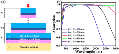
In this paper, we design the stacking structure of multi-cycle absorber units as shown in Fig. 1. We stack the first layer of absorber units on the refractory substrate W, both with a period of P1 = 250 nm, and the first layer of absorber units acts as the last recirculating cavity for the incident light to reach the absorber, which greatly enhances the light trapping ability. The periods of the absorber units of the second, third, fourth, and fifth layers are also sequentially reduced according to the optimal difference of 50 nm in our simulation, with periods of P2 = 200 nm, P3 = 150 nm, P4 = 100 nm, and P5 = 50 nm, respectively. The thicknesses of the individual square thin films in the modelled structure are shown in Fig. 2(a), in which the thickness of the substrate W is H1 = 150 nm, and a certain thickness is used to prevent light transmission, and the thicknesses of TiN, InAs, and SiO2 in an absorber are H2 = 20 nm, H3 = 10 nm, and H4 = 100 nm, in that order, which are used as the core part of the absorber to achieve high performance. And sequentially stacking the first layer of absorption units N1 up to the fifth layer N5. We used FDTD to calculate the structure, and we set the wavelength range of incident light from above the Z-axis to be 280 nm–3000 nm, covering the visible, ultraviolet, near-infrared, and mid-infrared wavelength segments. With periodic boundary conditions in the X and Y directions, we make perfectly matched layers in the Z direction, on the other hand, also set the mesh accuracy in the simulation to 5.31–33 The dielectric constants of W, TiN, InAs, and SiO2 were taken from Palik.34 The optical absorption can be expressed as A = 1-T-R. Since the substrate W is impervious to light, indicating T = 0, then the absorptivity can be expressed as A = 1-R.35,36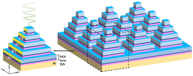 | ||
| Fig. 1 Designed solar absorber structure where P1 = 250 nm, P2 = 200 nm, P3 = 150 nm, P4 = 100 nm, P5 = 50 nm. | ||
3. Results and discussion
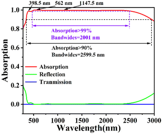
In order to find the optimal absorber for the absorber with the number of layers i of the absorber unit and the corresponding period P1, we sequentially stack the absorber unit Ni and discuss the corresponding absorption map, where the stacking operation flow is shown in Fig. 2(a). While stacking the absorbing units, we make the absorbing unit period Pi of two neighboring layers always keep a difference of 50 nm. So, when we increase the common period P1 of the substrate W and the first absorber unit N1 layer by layer, when P1 = 150 nm, 200 nm, 250 nm, 300 nm, and 350 nm, the corresponding absorber unit layers will also be increased, respectively, and the number of stacked layers will be i = 3, 4, 5, 6, and 7 in order, and the final absorption effect will be shown in Fig. 2(b). When i = 3, the absorption efficiency is not efficient, and the absorption in the near-infrared band after 1500 nm shows a steep drop. When i = 4, the absorption at 280 nm–3000 nm is greatly improved with an average absorption of 92.58%, but the bandwidth of its perfect band (A > 90%) is only 2016 nm (366 nm–2382 nm), while the absorption in the near-infrared band after 2000 nm gradually decreases, which is not enough to emphasize the excellence of our designed absorber. So, we need to expand the bandwidth and increase the overall stability of our absorber to emphasize its excellence, we further increase the period to P1 = 250 nm and the number of layers to i = 5, at which time the absorber has a continuous ultra-perfect band (A > 99%) with a bandwidth of 2001 nm (477.5 nm–2478.5 nm) and an average absorption of 98.24% at 280 nm–3000 nm. Compared to the absorption spectra at i = 6 and 7, we consider i = 5 and P1 = 250 nm to be the best parameters for achieving high absorber performance. This is because when i = 6 and 7, as can be seen in Fig. 2(b), the increase in the number of layers i is very effective and significantly extends the absorption bandwidth. However, the absorption efficiency is unstable in the range of 280 nm–3000 nm, and there is no continuous A > 99%, which is not the desired result.When i = 5 with P1 = 250 nm is determined, we give its absorption, reflection, and transmission spectra in Fig. 3 in order to get the absorption results in detail for the absorber's ultra-bandwidth, which can be analyzed to show that the absorber achieves an average absorption of 98.24% in the given bands 280 nm–3000 nm and an absorption A > 90% in the band 346.5 nm–2946 nm. It is noteworthy that the bandwidth of 2100 nm (477.5 nm–2478.5 nm) is an ultra-perfect band range in which the absorption is constant at greater than 99%. Therefore, it has unrivaled high absorption performance for visible and near-infrared light, with the main absorption losses concentrated in the invisible ultraviolet and mid-infrared bands.37–39
Meanwhile, we selected the three absorption peaks (λ1 = 398.5 nm, λ2 = 562 nm, and λ3 = 1147.5 nm) given in Fig. 3, which have absorptivity of 98.773%, 99.967%, and 99.716%, respectively. As shown in Fig. 4, at three wavelengths, we calculated the electric field distributions for different cross sections (XOY and XOZ sections), which allowed us to better explore further the physical mechanisms of the absorbers achieving high absorption in the UV, VIS, and NIR bands, respectively.
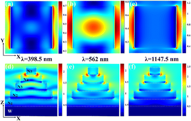 | ||
| Fig. 4 (a)–(c) in the XOY plane, show the electric field distribution of the absorber. (d)–(f) in the XOZ plane, show the electric field distribution of the absorber. | ||
Fig. 4(a) and (d) shows that at λ1 = 398.5 nm, the electric field is mainly concentrated at the corners of the fourth layer N4 and the fifth layer absorber unit N5 as well as on the surface of each absorber unit, while the intensity is also manifested in the inner part of each absorber unit, so we can assume that the strong absorption of the absorber in UV is related to the SPR at the connecting corners of absorber units.40,41 The wavelength of visible light λ2 = 562 nm is selected, and as in Fig. 4(b) and (e), the hot spot of the electric field is gradually distributed to the corners of the absorber units below and is no longer confined to the top absorber unit, while the interaction between the Fabry–Perot resonant cavities in the interior of the absorber units42,43 is strengthened, and the coupling between each other causes the absorption of the visible light to reach the peak. As shown in Fig. 4(c) and (f), at λ3 = 1147 nm, the electric field hotspots at the corners of the five-layer absorber units of the absorber are further enhanced, but due to the weakening of the internal resonance effect of the absorber units, the overall average absorption in the NIR band is not as excellent as that of the visible light, but the overall absorption is still maintained at A > 99%, which cannot be separated from the centralized distribution of the electric field at the corners of the various absorber units, which excites equipartition excitation resonance, which maintains the absorption under the broadband.44,45 It can be seen that the physical mechanism of the absorber to achieve high absorption in the UV, VIS, and NIR bands, respectively, is due to the surface plasmon action at the corners of the film at each absorber cell and the internal resonant coupling between neighboring absorber cells.
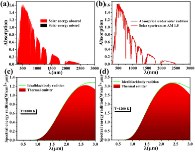
In order to simulate the spectral distribution of sunlight irradiated onto a solar absorber under ideal AM1.5 conditions, we give the total spectral equation for AM1.5 incident solar energy in eqn (1):46,47
 | (1) |
On the other hand, in order to investigate the thermal radiation efficiency when the absorber acts as a thermal radiator, we define the thermal radiation efficiency as in eqn (2):51
 | (2) |
| Ref. | Absorbing material | Average absorption rate | Thermal efficiency |
|---|---|---|---|
| 52 | Ti-AlO-Ti-W-Ti-AlO | 95.8% (200 nm–3100 nm) | 94.4% (1000 K) |
| 53 | Ti-Al2O3 | 98.78% (385 nm–1765 nm) | Not mentioned |
| 54 | InAs-Ti-W-Ti-AlO | 95.80% (283 nm–3615 nm) | 95.42% (1000 K) |
| 55 | Ti-GaAs | 96.52% (300 nm–4000 nm) | >90% (373 K–973 K) |
| 56 | Ti | 97.85% (200 nm–2980 nm) | >90% (373 K–1073 K) |
| Our work | SiO2-InAs-TiN-W | 98.24% (280 nm–3000 nm) | 97.83% (1200 K) |
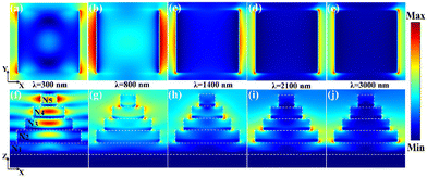
In order to investigate the SPR resonant coupling phenomena between the Fabry–Perot resonance cavities between the absorber's multiple cycles of absorber units and the corners of each connection under the whole wavelength band, here, at five wavelengths, we provide the electric field strength distributions of the absorber cross sections XOY and XOZ (λ = 300 nm, 800 nm, 1400 nm, 2100 nm, 3000 nm) as shown in Fig. 6. Fig. 6(a) and (f) shows the electric field distributions in the XOY cross section and XOZ cross section of the absorber at λ = 300 nm when the Fabry–Perot resonance phenomenon excited in the SiO2 films inside the absorber cells N1 to N5 is significant and the electric field strength gradually decays from the top absorber cell N5 to the last absorber cell N1. Fig. 6(b), (g) and (c), (h) show the electric field intensity at λ = 800 nm and 1400 nm, respectively, and it can be observed that the Fabry–Perot resonance excited in the SiO2 films inside the absorber units N1 to N5 at this time decreases, which is less significant than that of the wavelength of 300 nm. There is a hot spot of electric field in the corner of the SiO2 and TiN films in absorber units N4 and N5, and the ultra-broadband absorption at this time is determined by the weak Fabry–Perot resonance coupling effect between SPR and absorber units at the corner of N4 and N5.57 As incident light wavelength increases, the electric field hotspot gradually shifts to the bottom of the absorber at λ = 2100 nm and 3000 nm, as shown in Fig. 6(d), (i) and (e), (j). It is mainly concentrated at the corners where the SiO2 film and TiN film in the absorber units N2 and N3 are connected. In other words, the Fabry–Perot resonance effect between the absorber units is no longer obvious, and at this time, we can think that the stable absorption in the 2100 nm–3000 nm band is maintained by the SPR effect at the corners of N2, N3.
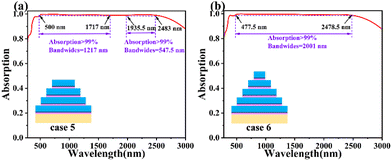
We have also given six different absorber structures in this work to discuss their absorption spectra, as shown in Fig. 7 and 8. Cases 1, 2, and 3 in Fig. 7(b) show the number of layers of absorber units increasing sequentially from i = 1 up to i = 3 at a period P1 = 250 nm. It can be concluded from Fig. 7(a) that the more layers of absorber units are added, the closer the absorber comes to high efficiency absorption, and when there are 3 layers of absorber units, the absorber achieves continuous high efficiency absorption in the visible-near infrared band at this time (A > 90%), but it is far from achieving A > 90% for a bandwidth of 2001 nm. 90% in the visible and near-infrared wavelength bands, but it is still far from achieving A > 99% with a bandwidth of 2001 nm. In case 4, the absorber units N1–N5 all have the same period and are sequentially superimposed on the refractory metal W. In case 4, the number of absorber layers i is the same as that in case 4, which is the same as that in case 4. That is, the number of absorbing layers i = 5 in case 4, but the absorption effect does not improve with the increase in the number of layers i. Instead, the absorption effect is unsatisfactory, and there is no stable absorption. This is due to the fact that the period of each absorbing unit is the same, so that the SPR is suppressed at the connection of each corner. As shown in Fig. 8(a) and (b), cases 5 and 6 have the same structural parameters and similar absorption effects, with the difference that case 6 has only one more absorber unit cavity, N5, than case 5. Therefore, in order to investigate the role of the absorber unit N5 on the absorber, we have analyzed the absorption spectra of cases 5 and 6 separately. Fig. 8(a) shows that case 5 exhibits excellent absorption in the 500 nm–1717 nm and 1935.5 nm–2483 nm bands, with a total bandwidth of 1764.5 nm for A > 99%, while case 6 has a continuous and ultra-perfect absorption in the 477.5 nm–2478.5 nm bands, with an astonishing bandwidth of 2001 nm. The physical mechanism behind the small absorption difference is reflected in the fact that case 5 has a very high A > 99% absorption. The physical mechanism behind the difference in absorption is reflected in the SPR at the corner of the top absorber N5, which also suggests that it is necessary to choose case 6 with one more layer of absorber N5.
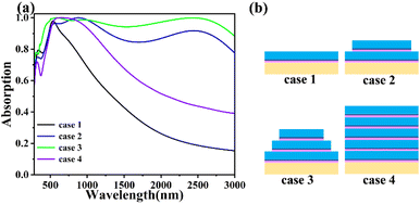 | ||
| Fig. 7 (a) Absorption diagrams for four cases of absorber. (b) Models corresponding to the absorber in the four cases. | ||
In order to further investigate whether our designed absorber can be replaced by other high-temperature-resistant materials, the absorption spectra of different materials are investigated here. As shown in Fig. 9(b), the absorber unit in case 7 consists of SiO2-In-TiN film. Compared with case 6, the absorber has obvious absorption peaks at this time, but the absorption after the wavelength of 2000 nm is unsatisfactory, which also indicates that it is necessary for us to choose the thinnest square InAs film in the absorber parameters as the composition of the Fabry–Perot cavity.58,59 Meanwhile, monocrystalline arsenic is toxic and is not suitable for direct production and use in practical applications. In case 8, we replace the SiO2 film in case 6 with TiN film, and the absorption effect is extremely poor in the wavelength band after the visible light. This is because the TiN-In-TiN film of the absorber cell in case 8 does not form a Fabry–Perot resonance cavity, and then the high absorption efficiency, which is determined by the coupling of SPR at the corners and Fabry–Perot resonance of absorber cells, does not exist. Performance also does not exist. We replaced the TiN film in case 6 with a Ti film in case 9. Case 9 still absorbs very well, achieving A > 90% in the 2293 nm bandwidth. However, as the wavelength increases, the SPR effect of the Ti-SiO2 films at the junction of the individual absorption units decreases and is not as excellent as the SPR effect between the TiN-SiO2 films. Analyzing the absorption spectra above, it is clear that the structure and materials we propose have excellent absorption and are irreplaceable.
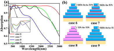 | ||
| Fig. 9 (a) Absorption diagrams for four different material cases. (b) are the schematic diagrams corresponding to the four different materials in (a). | ||
We also analyzed the effect of the thickness H2 of the TiN film in the absorber cell versus the thickness H4 of the SiO2 film on the absorber. As shown in Fig. 10(a) and (b), by increasing H2 from 10 nm to 30 nm and H4 from 60 nm to 140 nm, it can be seen that the bandwidth of the perfect absorption (A > 90%) also increases, which is due to the increase of H2, H4, which increases the spacing of the Fabry–Perot resonance cavities between the absorber cells, and the plasmonic effect is enhanced.60,61 Although the increase in the thickness of TiN film and SiO2 film helps to expand the absorption bandwidth, it does not mean that the larger values of H2 and H4 are better, and we need to choose the H2 and H4 parameters for stable absorption. When H4 = 100 nm and H2 is greater than 20 nm and less than 25 nm, the absorption is shown in Fig. 10(a). In the near-infrared band, we think that the difference between the red and green line absorption is not obvious at this time, and either H2 = 20 nm or 25 nm can satisfy our requirements, which is an acceptable range of error for the production of TiN films. When H4 = 100 nm and H2 = 30 nm, the absorption bandwidth is further expanded, but continuous ultra-perfect absorption cannot be achieved in the whole band (280 nm–3000 nm). As shown in Fig. 10(b), in mid-infrared bands, the effective bandwidth of the absorber increases when H2 = 20 nm and H4 = 60 nm to 140 nm, but the absorption is the most stable under the whole band only when H4 = 100 nm, which can achieve A > 99% under the maximum bandwidth. Therefore, finally, we determined that H2 = 20 nm and H4 = 100 nm are the optimal operating parameters.
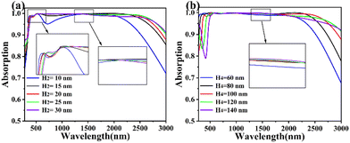 | ||
| Fig. 10 (a) The thickness of TiN film H2 was increased from 10 nm to 30 nm in 5 nm intervals. (b) The thickness of SiO2 film H4 was increased from 60 nm to 140 nm at 20 nm intervals. | ||
The complexity of the environment makes it necessary for broadband absorbers to meet the requirements of being polarization-independent and insensitive to large-angle (0°–60°) sunlight incidence.62–66 For this reason, we designed a symmetric absorber structure, which has the same absorption spectrum in TE-polarized mode and TM-polarized mode, as shown in Fig. 11(a). Meanwhile, in the absorption scan plot from TM polarization to TE polarization, the absorption spectra remain constant as the polarization angle increases from 0° to 90°, as shown in Fig. 11(b). This confirms the polarization-independent property of the absorber. To investigate the absorption of the absorber at large incidence angles in TE and TM, we give here the formal plots of polarization in TE and TM modes as shown in Fig. 12(a) and (b), where the TE polarization is shown as the direction of the electric field of the sunlight along the Y-direction of the space and the TM polarization is shown as the direction of the electric field of the sunlight along the X-direction of the space. From Fig. 12(c) and (d), from 0° to 60°, the incidence angle of sunlight increases, the absorption effect graphs of TE and TM are identical, and at the same time, in both TE and TM modes, even though the incidence angle is increased to 60°, at this time, the absorber still achieves the effect of A > 90% in the 280 nm–2185.5 nm band, and the average absorption rate in the whole band reaches 90.83%. Therefore, we believe that the absorber appears to be independent of the polarization of sunlight and insensitive to large angles of incidence, but still has excellent results and can be applied to more complex environments.
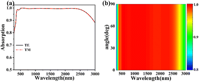 | ||
| Fig. 11 (a) Absorber uptake in TE and TM modes. (b) Normalized absorption spectra for TM polarization to TE polarization (increase in polarization angle from 0° to 90°). | ||
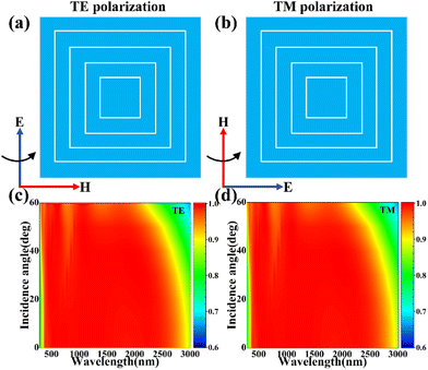 | ||
| Fig. 12 (a) and (b) Schematic of TE and TM polarization modes. (c) and (d) Absorption spectra for TE and TM polarizations with increasing angles of incidence from 0°–60°. | ||
4. Conclusion
In conclusion, we have designed a solar absorber that is based on a stacked structure of five-layer absorber units with regularly decreasing periods, where the SiO2-InAs-TiN three-layer film is one absorber unit. The SPR at the corner of each absorber unit and the Fabry–Perot resonance coupling between the absorber units are the physical mechanisms to achieve the high absorption efficiency, so that the absorber achieves an average absorption of 98.24% over the whole band (280 nm–3000 nm), with a bandwidth of 2599.5 nm for A > 90%, of which the bandwidth is 2001 nm for A > 99%. The weighted absorption over the entire band is 99.31%, with less than 1% energy loss. When used as an emitter, the thermal radiation efficiency reaches 97.35% and 97.83% at 1000 K and 1200 K, respectively. On the other hand, normalized absorption spectrum from TM to TE polarization does not change with polarization angle due to the symmetric structure of the absorber, and the absorber still achieves A > 90% in the 280 nm–2185.5 nm band with an average absorption of 90.83%, even if the incidence angle of the sunlight is increased to 60° in both TE- and TM-polarized modes.Data availability
The data are available from the corresponding author on reasonable request.Conflicts of interest
There are no conflicts to declare.Acknowledgements
The authors are grateful to the support by National Natural Science Foundation of China (No. 51606158, 11604311, 12074151); the Funded by the Guangxi Science and Technology Base and Talent Special Project (No. AD21075009); the funded by the Sichuan Science and Technology Program (No. 2021JDRC0022); the funded by the Natural Science Foundation of Fujian Province (2021J05202); the funded by the Research Project of Fashu Foundation (MFK23006); the funded by the Open Fund of the Key Laboratory for Metallurgical Equipment and Control Technology of Ministry of Education in Wuhan University of Science and Technology, China (No. MECOF2022B01; MECOF2023B04); the funded by the Project supported by Guangxi Key Laboratory of Precision Navigation Technology and Application, Guilin University of Electronic Technology (No. DH202321); the funded by the Scientific Research Project of Huzhou College (2022HXKM07).References
- T. X. Xiao, S. Tu, S. Z. Liang, R. J. Guo and T. Tian,
et al.
, Opto-Electron. Sci., 2023, 2, 230011 CAS
.
- Q. C. Han, S. W. Liu, Y. Y. Liu, J. S. Jin, D. Li, S. B. Cheng and Y. Xiong, Sol. Energy, 2020, 208, 469–479 CrossRef CAS
.
- M. Baeva, D. Gets, A. Polushkin, A. Vorobyov and A. Goltaev,
et al.
, Opto-Electron. Adv., 2023, 6, 220154 CAS
.
- J. Maksimovic, J. W. Hu, S. H. Ng, T. Katkus and G. Seniutinas,
et al.
, Opto-Electron. Adv., 2022, 5, 210086 CAS
.
- Y. Zheng, W. C. o Zhao, Q. J. Song, C. Ma, Z. Yi, Q. D. Zeng, T. Y. Sun, J. X. Chen and J. Q. Yan, Int. J. Therm. Sci., 2024, 203, 109172 CrossRef CAS
.
- F. Y. Wu, Y. H. Liu, L. Ling, Z. X. Sheng, Z. Yi, Q. J. Song, S. B. Cheng, B. Tang, S. Ahmad and T. Y. Sun, Adv. Photonics Res., 2024, 5(3), 2300305 CrossRef CAS
.
- E. Serpetzoglou, I. Konidakis, G. Kourmoulakis, I. Demeridou and K. Chatzimanolis,
et al.
, Opto-Electron. Sci., 2022, 1, 210005 CAS
.
- H. Zhang, L. Feng, F. Y. Wang, M. Z. Liu and Y. Y. Zhang,
et al.
, Opto-Electron. Adv., 2023, 6, 220061 CAS
.
- D. Z. Tan, K. Sun, Z. L. Li, B. B. Xu and J. R. Qiu, Photo-processing of perovskites: current research status and challenges, Opto-Electron. Sci., 2022, 1, 220014 CAS
.
- H. Xiong, X. Ma, B. X. Wang and H. Zhang, Sens. Actuators, A, 2024, 366, 114972 CrossRef CAS
.
- A. Elbanna, K. Chaykun, Y. Lekina, Y. D. Liu and B. Febriansyah,
et al.
, Opto-Electron. Sci., 2022, 1, 220006 CAS
.
- Y. Zheng, Z. Y. Wang, Z. Yi, S. B. Cheng, C. Ma, B. Tang, T. Y. Sun, S. J. Yu, G. F. Li and S. Ahmad, Diamond Relat. Mater., 2024, 142, 110843 CrossRef CAS
.
- L. Wu, L. L. Yang, X. W. Zhu, B. Cai and Y. Z. Cheng, Int. J. Therm. Sci., 2024, 201, 109043 CrossRef CAS
.
- T. Zhang, S. J. Wang, X. Y. Zhang, M. Fu, Y. Yang, W. Chen and D. Su, Front. Chem. Sci. Eng., 2020, 15, 35–48 CrossRef
.
- H. Xiong, X. D. Ma, H. S. Liu, D. P. Xiao and H. Q. Zhang, Appl. Phys. Lett., 2023, 123, 153902 CrossRef CAS
.
- H. Xiong, M. Suo, X. K. Li, D. P. Xiao and H. Q. Zhang, ACS Appl. Electron. Mater., 2024, 6(2), 696–701 CrossRef CAS
.
- S. Patial, P. Raizada, V. Hasija, P. Singh, V. K. Thakur and V. H. Nguyen, Mater. Today Energy, 2021, 19, 100589 CrossRef CAS
.
- H. T. Liu, K. Yu, K. H. Zhang, Q. Ai, M. Xie and X. H. Wu, Phys. Chem. Chem. Phys., 2023, 25, 10628–10634 RSC
.
- C. Gehrmann and D. A. Egger, Nat. Commun., 2019, 10, 3141 CrossRef
.
- S. R. Liang, S. B. Cheng, H. F. Zhang, W. X. Yang, Z. Yi, Q. D. Zeng, B. Tang, P. H. Wu, S. Ahmad and T. Y. Sun, Ceram. Int., 2024, 50, 23611–23620 CrossRef CAS
.
- K. T. Lin, H. Lin, T. Yang and B. Jia, Nat. Commun., 2020, 11, 1389 CrossRef CAS PubMed
.
- Z. Liu, G. Liu, Z. Huang, X. Liu and G. Fu, Sol. Energy Mater. Sol. Cells, 2018, 179, 346–352 CrossRef CAS
.
- F. Qin, X. Chen, Z. Yi, W. Yao, H. Yang, Y. Tang, Y. Yi, H. Li and Y. Yi, Sol. Energy Mater. Sol. Cells, 2020, 211, 110535 CrossRef CAS
.
- W. X. Li, M. S. Liu, S. B. Cheng, H. F. Zhang, W. X. Yang, Z. Yi, Q. D. Zeng, B. Tang, S. Ahmad and T. Y. Sun, Diamond Relat. Mater., 2024, 142, 110793 CrossRef CAS
.
- C. Gigli and G. Leo, Opto-Electron. Adv., 2022, 5, 210093 CAS
.
- W. X. Li, J. Ma, H. F. Zhang, S. B. Cheng, W. X. Yang, Z. Yi, H. Yang, J. G. Zhang, X. W. Wu and P. H. Wu, Phys. Chem. Chem. Phys., 2023, 25, 8489–8496 RSC
.
- N. Xu, J. Li, Y. Wang, C. Fang, X. Li, Y. Wang, L. Zhou, B. Zhu, Z. Wu and S. Zhu, Sci. Adv., 2019, 5, eaaw7013 CrossRef CAS PubMed
.
- T. A. Cooper, S. H. Zandavi, G. W. Ni, Y. Tsurimaki, Y. Huang, S. V. Boriskina and G. Chen, Nat. Commun., 2018, 9, 5086 CrossRef CAS PubMed
.
- M. Chen and Y. He, Sol. Energy Mater. Sol. Cells, 2018, 188, 156–163 CrossRef CAS
.
- E. Cortés, F. J. Wendisch, L. Sortino, A. Mancini, S. Ezendam, S. Saris, L. de S. Menezes, A. Tittl, H. Ren and S. A. Maier, Chem. Rev., 2022, 122, 15082–15176 CrossRef PubMed
.
- W. X. Li, W. C. Zhao, S. B. Cheng, H. F. Zhang, Z. Yi, T. Y. Sun, P. H. Wu, Q. D. Zeng and R. Raza, Opt. Lasers Eng., 2024, 181, 108368 CrossRef
.
- R. Fu, K. X. Chen, Z. L. Li, S. H. Yu and G. X. Zheng, Opto-Electron. Sci., 2022, 1, 220011 CAS
.
- S. R. Liang, F. Xu, W. X. Li, W. X. Yang, S. B. Cheng, H. Yang, J. Chen, Z. Yi and P. P. Jiang, Appl. Therm. Eng., 2023, 232, 121074 CrossRef CAS
.
-
E. D. Palik, Handbook of Optical Constants of Solids I–III, Academic Press, Orlando, FL, USA, 1998 Search PubMed
.
- W. T. Buono and A. Forbes, Opto-Electron. Adv., 2022, 5, 210174 CAS
.
- T. Sang, Q. Mi, C. Y. Yang, X. H. Zhang, Y. K. Wang, Y. Z. Ren and T. Xu, Nanophotonics, 2024, 13(8), 1369–1377 CrossRef CAS
.
- H. Y. Guan, J. Y. Hong, X. L. Wang, J. Y. Ming, Z. L. Zhang, A. J. Liang, X. Y. Han, J. L. Dong, W. T. Qiu, Z. Chen, H. H. Lu and H. Zhang, Adv. Opt. Mater., 2021, 9(16), 2100245 CrossRef CAS
.
- S. R. Liang, F. Xu, H. Yang, S. B. Cheng, W. X. Yang, Z. Yi, Q. J. Song, P. H. Wu, J. Chen and C. J. Tang, Opt. Laser Technol., 2023, 158, 108789 CrossRef CAS
.
- H. R. Xie, T. F. Yang, M. Y. Xie, X. J. Liang, Z. L. Fang, Y. Ye, Y. Chen, Y. M. Wei, Z. Wang, H. Y. Guan and H. H. Lu, Laser Photonics Rev., 2024, 18(5), 2301129 CrossRef CAS
.
- W. X. Li, S. B. Cheng, H. F. Zhang, Z. Yi, B. Tang, C. Ma, P. H. Wu, Q. D. Zeng and R. Raza, Commun. Theor. Phys., 2024, 76, 065701 CrossRef
.
- J. Ma, P. H. Wu, W. X. Li, S. R. Liang, Q. Y. Shangguan, S. B. Cheng, Y. H. Tian, J. Q. Fu and L. B. Zhang, Diamond Relat. Mater., 2023, 136, 109960 CrossRef CAS
.
- S. B. Cheng, T. Xia, M. S. Liu, S. Xu, S. F. Gao, G. Zhang and S. H. Tao, Opt. Laser Technol., 2019, 117, 288–292 CrossRef
.
- T. X. Zhang, C. Tao, S. X. Ge, D. W. Pan, B. Li, W. X. Huang, W. Wang and L. Y. Chu, Chem. Eng. J., 2022, 434, 134769 CrossRef CAS
.
- J. Luo, Results Phys., 2024, 60, 107667 CrossRef
.
- W. X. Li, Y. H. Liu, L. Ling, Z. X. Sheng, S. B. Cheng, Z. Yi, P. H. Wu, Q. D. Zeng, B. Tang and S. Ahmad, Surf. Interfaces, 2024, 48, 104248 CrossRef CAS
.
- S. Li, T. Sang, C. Y. Yang, J. J. Lu and Y. K. Wang, Opt. Lett., 2023, 48(24), 6488–6491 CrossRef CAS PubMed
.
- S. Ishii, S. L. Shinde, W. Jevasuwan, N. Fukata and T. Nagao, ACS Photonics, 2016, 3, 1552–1557 CrossRef CAS
.
- T. Shui, X. M. Chen and W. X. Yang, Appl. Opt., 2022, 61(34), 10072–10079 CrossRef PubMed
.
- Q. Y. Shangguan, Y. Zhao, Z. J. Song, J. Wang, H. Yang, J. Chen, C. Liu, S. B. Cheng, W. X. Yang and Z. Yi, Diamond Relat. Mater., 2022, 128, 109273 CrossRef CAS
.
- W. X. Li, F. Xu, S. B. Cheng, W. X. Yang, B. Liu, M. S. Liu, Z. Yi, B. Tang, J. Chen and T. Y. Sun, Opt. Laser Technol., 2024, 169, 110186 CrossRef CAS
.
- M. M. Gao, L. L. Zhu, C. K. Peh and G. W. Ho, Energy Environ. Sci., 2019, 12, 841–864 RSC
.
- F. Wu, P. Shi, Z. Yi, H. Li and Y. Yi, Micromachines, 2023, 14, 985 CrossRef PubMed
.
- Y. J. Zhang, Y. T. Yi, W. X. Li, S. R. Liang, J. Ma, S. B. Cheng, W. X. Yang and Y. G. Yi, Coatings, 2023, 13(3), 531 CrossRef CAS
.
- Y. Zhu, P. Cai, W. Zhang, T. Meng, Y. Tang, Z. Yi, K. Wei, G. Li, B. Tang and Y. Yi, Micromachines, 2023, 14, 1597 CrossRef PubMed
.
- J. Wang, H. Feng and Y. Gao, Laser Phys., 2024, 34, 025901 CrossRef
.
- J. Zhou, Z. Liu, G. Liu, P. Pan, X. Liu, C. Tang, Z. Liu and J. Wang, Opt. Express, 2020, 28, 36476–36486 CrossRef CAS PubMed
.
- W. X. Li, W. C. Zhao, S. B. Cheng, W. X. Yang, Z. Yi, G. F. Li, L. C. Zeng, H. L. Li, P. H. Wu and S. S. Cai, Surf. Interfaces, 2023, 40, 103042 CrossRef CAS
.
- Y. X. Zhang, M. B. Pu, J. J. Jin, X. J. Lu and Y. H. Guo,
et al.
, Opto-Electron. Adv., 2022, 5, 220058 CAS
.
- Q. Y. Shangguan, Z. H. Chen, H. Yang, S. B. Cheng, W. X. Yang, Z. Yi, X. W. Wu, S. F. Wang, Y. G. Yi and P. H. Wu, Sensors, 2022, 22, 6483 CrossRef CAS PubMed
.
- W. X. Li, Y. T. Yi, H. Yang, S. B. Cheng, W. X. Yang, H. F. Zhang, Z. Yi, Y. G. Yi and H. L. Li, Commun. Theor. Phys., 2023, 75, 045503 CrossRef
.
- Q. Y. Shangguan, H. Chen, H. Yang, S. R. Liang, Y. J. Zhang, S. B. Cheng, W. X. Yang, Z. Yi, Y. Luo and P. H. Wu, Diamond Relat. Mater., 2022, 125, 108973 CrossRef CAS
.
- J. W. Lv, W. Li, J. X. Wang, X. L. Lu, Q. Li, Y. R. Ren, Y. Yu, Q. Liu, P. K. Chu and C. Liu, Opt. Express, 2024, 32(11), 19057–19068 CrossRef PubMed
.
- S. Krasikov, A. Tranter, A. Bogdanov and Y. Kivshar, Opto-Electron. Adv., 2022, 5, 210147 CAS
.
- Z. L. Li, M. X. Xie, G. Z. Nie, J. H. Wang and L. J. Huang, J. Phys. Chem. Lett., 2023, 14, 10762–11076 CrossRef CAS PubMed
.
- J. H. Deng, H. Xiong, Q. Yang, M. Suo, J. Y. Xie and H. Q. Zhang, IEEE Sens. J., 2023, 23(19), 22459–22465 Search PubMed
.
- H. Xiong, J. Deng, Q. Yang, B. X. Wang, X. Wang and H. Zhang, ACS Appl. Electron. Mater., 2024, 6(2), 1204–1210 CrossRef CAS
.
| This journal is © The Royal Society of Chemistry 2024 |

