 Open Access Article
Plasma-assisted fabrication of ultra-dispersed copper oxides in and on C-rich carbon nitride as functional composites for the oxygen evolution reaction†
Mattia
Benedet
 ab,
Angelica
Fasan
b,
Davide
Barreca
 b,
Chiara
Maccato
 *ab,
Cinzia
Sada
 c,
Silvia Maria
Deambrosis
 b,
Valentina
Zin
b,
Francesco
Montagner
b,
Oleg I.
Lebedev
d,
Evgeny
Modin
e,
Gian Andrea
Rizzi
b,
Valentina
Zin
b,
Francesco
Montagner
b,
Oleg I.
Lebedev
d,
Evgeny
Modin
e,
Gian Andrea
Rizzi
 ab and
Alberto
Gasparotto
 ab
ab
aDepartment of Chemical Sciences, Padova University and INSTM, 35131 Padova, Italy. E-mail: chiara.maccato@unipd.it
bCNR-ICMATE and INSTM, 35127 Padova, Italy
cDepartment of Physics and Astronomy, Padova University and INSTM, 35131 Padova, Italy
dLaboratoire CRISMAT, UMR 6508 Normandie Université, CNRS, ENSICAEN, UNICAEN, 14050 Caen Cedex 4, France
eCIC nanoGUNE BRTA, 20018 Donostia, San Sebastian, Spain
First published on 23rd September 2024
Abstract
Significant efforts have been continuously devoted to the mastering of green catalysts for the oxygen evolution reaction (OER), whose sluggish kinetics prevents a broad market penetration of water splitting as a sustainable route for large-scale hydrogen production. In this extensive scenario, carbon nitride (CN)-based systems are in focus thanks to their favorable characteristics, and, whereas graphitic CN has been largely investigated, the potential of amorphous carbon nitride (a-CNx) systems remains almost entirely unexplored. In this regard, our study presents a novel two-step plasma-assisted route to a-CNx systems comprising ultra-dispersed, i.e. “quasi-atomic” CuxO (x = 1, 2). The target materials were fabricated using an original strategy consisting in the magnetron sputtering of a-CNx on conducting glasses at room temperature, followed by functionalization with low CuxO amounts by radio frequency (RF)-sputtering, and final annealing under an inert atmosphere. The tailoring of the CuxO co-catalyst content and spatial dispersion, as well as the overall composite features as a function of preparative conditions, enabled a direct modulation of the resulting OER performances, rationalized based on the formation of p-n CuxO/a-CNx heterojunctions. The amenable and scalable synthesis approach underscores the practicality of this method to develop (photo)electrocatalysts synergistically integrating the advantages of both constituents, yielding low-cost, green, and stable functional platforms that could contribute to the broader adoption of sustainable energy solutions.
1. Introduction
Meeting the ever-growing global energy demand in an environmentally friendly manner, especially starting from renewable sources, is of paramount importance to promote a greener economic and social growth in the actual scenario.1 As an alternative to the unsustainable use of fossil fuels, green hydrogen has gained strategic interest as a clean energy vector for the transformation of the future energy landscape.2–7 Among the various processes for its production, electrochemical water splitting (WS), eventually activated by solar light, has attracted worldwide attention for a possible large-scale H2 generation free from any harmful emission.2,8–11 Nevertheless, the energy conversion efficiency is limited by the barrier associated with the anodic oxygen evolution reaction (OER), the actual WS bottleneck, constituting a main source of energy loss.5,12–14 To counteract the sluggish OER kinetics and bypass complex multi-electron reaction pathways, the use of active and stable electrocatalysts is mandatory, and the shortcomings of state-of-the-art systems based on noble metals15–17 make the implementation of efficient, green, and economically viable catalysts an imperative task.3,9 In the current tide of possible candidates, graphitic carbon nitride (g-CN)-based ones have been the subject of several studies thanks to their excellent chemical stability, high biocompatibility, Vis light absorption, and tunable electronic structure.12,13,15,17–19Beyond g-CN, even other C-based N-containing materials, such as N-doped graphene/graphite and various forms of nano-carbon films and nanosystems, have come under intense scrutiny for green applications, which include (photo)catalysts for pollutant degradation, CO2 reduction, and H2 production.16,20–23 In this context, amorphous carbon nitride (a-CNx) systems (often improperly termed N-doped carbon), with an atomic N/C ratio lower than that of stoichiometric C3N4,24 feature a strong covalently bonded network,25 resulting in marked chemical stability,26 remarkable hardness and elasticity,27–29 and improved wear durability.30 These materials have been investigated for the fabrication of protective coatings,31–33 sensors,34 and various functional devices.26,35–37 Despite a-CNx possessing an improved photocatalytic activity in H2 evolution, due to its wider light absorption range and quenched recombination phenomena,22 its utilization as a (photo)electrocatalyst has only seldom been reported so far.16,38 One of the reasons is that its thermal stability and atomic level-structure are still poorly known,30 mainly due to the rich variety of possible local environments and the lack of long-range order.37,39,40 The characteristics of a-CNx materials are directly dependent on their microstructure and nitrogen content,37,41 which, in turn, are affected by the used preparation strategy and processing conditions.29–31,42 To date, a-CNx films have been prepared using various techniques, such as pulsed laser ablation,28,37,42 magnetron sputtering,26,29–34,36,40,41 alternated reactive sputtering and etching,35 low-energy ion implantation,25 and ion-beam-assisted cathodic vacuum arc deposition.39
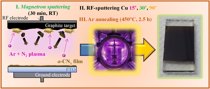
In this study, we have prepared CuxO-functionalized CNx-based films via an original multi-step plasma-assisted route (Fig. 1). The target procedure consisted in the magnetron sputtering of CNx onto fluorine-doped tin oxide (FTO) substrates at room temperature. Subsequently, ultra-low amounts of p-type copper oxides (CuxO; x = 1,2) were introduced by radio frequency (RF)-sputtering under mild conditions. The adopted process yielded an intimate contact between the two system components, which enabled their mutual interactions to promote a favorable modulation of the resulting functional properties.13,19,43 The fabricated materials possess higher mechanical stability than those obtained by powder immobilization as pastes/inks on various substrates,17,43 and are not affected by previously reported delamination problems.32,33
The choice of copper oxides as co-catalyst/functional activators is motivated by their natural abundance, non-toxicity, low cost, and band gaps enabling Vis-light absorption.8,44 In this regard, mixed Cu(I)–Cu(II) oxides offer higher stability, improved charge carrier transport kinetics, and enhanced light harvesting.43 Their combination with carbon nitride enables overcoming problems due to photocorrosion and benefitting from the controllable construction of heterojunctions, yielding broadened Vis radiation absorption and improved electron–hole separation.2,10,43,45,46 To date, CuxO-g-CN- and Cu-doped g-CN nanosystems, prepared by various techniques, have been proposed as (photo)catalysts for dye degradation,44 direct urea fuel cells,15 and H2 production,4,18,45 and (photo)cathodes for WS.2,3,8–10 Nonetheless, to the best of our knowledge, the use of CuxO/a-CNx as OER (photo)electrocatalysts has never been investigated so far.
This work provides a detailed investigation on these materials, with particular attention to a controllable CuxO ultra-dispersion. The latter issue relies on the fact that low-dimensional CuxO nanosystems with large surface areas and size-dependent features possess superior physico-chemical properties, remarkably differing from their micro- or bulk counterparts.47 In fact, the introduction of quantum dots of narrow band gap semiconductors (as Cu oxides), and of ultra-48,49 or atomically dispersed metal-based active sites,4,50,51 is a valuable route to enhance carbon nitride performances.45,52 The interplay between the latter and the chemico-physical properties of the materials was elucidated herein using a combined set of forefront analytical tools, enabling us to probe the structural, electronic, morphological, compositional, and mechanical characteristics. In particular, among the other characterization techniques, ion scattering spectroscopy (ISS) and reflection electron energy loss spectroscopy (REELS), used for the first time on similar systems, were associated with X-ray photoelectron spectroscopy (XPS). While ISS is specifically sensitive to the elemental composition of the outermost atomic layer,53 allowing us to directly probe the surface presence of low-sized CuxO nanoaggregates, REELS is an emerging technique to identify the presence of hydrogen,23,54 which, though being elusive, may significantly affect the properties and behaviors of the materials.
The obtained systems feature a close CuxO/a-CNx contact, as well as a CuxO loading/dispersion and nitrogen surface content controllable as a function of the sole RF-sputtering time. These variations resulted in the concomitant modulation of OER electrocatalytic activity, which, in turn, was directly dependent on CuxO spatial distribution. In particular, the best performances corresponded to an optimal compromise between an increased CuxO content and a suitable dispersion. These results, interpreted based on the formation of heterojunctions between the system components, were accompanied by a significant stability upon operation, which paves the way to eventual practical end-uses.
2. Experimental
Materials synthesis
After a pre-conditioning step (see § S1.1, ESI†), a-CNx deposits were obtained by employing a custom-built multiple-electrode apparatus equipped with a 13.56 MHz RF power supply. A pyrolytic graphite target (Nanovision Srl, thickness = 3 mm, diameter = 50 mm, purity = 99.999%) was fixed to a magnetron source and the coatings were grown from an electronic-grade Ar/N2 plasma. In each deposition, a pre-cleaned17 FTO substrate (2 × 1 cm2; Aldrich®; ≈7 Ω × sq−1; FTO thickness ≈ 600 nm) was mounted on the ground electrode. The growth procedure was performed without any preheating, under the following conditions: duration = 30 min; total pressure = 5.6 × 10⁻³ mbar; RF-power = 100 W; total Ar flow rate = 21 standard cubic centimeters per minute (sccm); total N2 flow rate = 42 sccm. After deposition, the samples were subjected to thermal treatment at 450 °C for 2.5 h under an argon atmosphere (heating rate = 2 °C min−1). Based on a series of preliminary optimization experiments, such an annealing treatment afforded an improvement of film adhesion to the substrate and its mechanical stability, a favorable issue in view of the target electrochemical applications. Under these conditions, no evidence of thermally-induced degradation of CNx deposits was ever detected, in line with previous studies.27,30,55,56Functionalization with copper oxides was performed by RF-sputtering from electronic-grade Ar plasma, using a custom-built two-electrode RF plasmochemical reactor (ν = 13.56 MHz). A copper target (Alfa Aesar®; thickness = 0.3 mm; purity = 99.95%) was mounted on the RF-electrode, whereas the FTO-supported carbon-rich CNx deposits were fixed on the grounded one. Based on previous results,57,58 depositions were carried out using the following settings: total pressure = 0.30 mbar; RF-power = 10 W; growth temperature = 60 °C; target–substrate distance = 60 mm; Ar flow rate = 10 sccm. The sputtering duration was set to 15, 30 and 90 min for samples labeled hereafter as CNx + Cu15, CNx + Cu30, and CNx + Cu90, respectively. Prior to chemico-physical characterization, the materials were annealed under Ar at 450 °C for 2.5 h. For comparison, RF-sputtering of the CuxO nanoparticles on bare FTO was also performed under the above reported conditions.
Materials characterization
FT-IR spectra were recorded in the 400–4000 cm−1 range on a JASCO 4100 instrument in diffuse reflectance (DRIFT) mode, using an EasiDiff specular beam collector (PIKE Technologies). Raman spectra were recorded using a Thermo-Fischer DXR Raman microscope equipped with a 532 nm laser (5 mW) focused on the sample with a 100X objective, obtaining a spot size of ≈1 μm. XPS, ultraviolet photoelectron spectroscopy (UPS), ISS, and REELS analyses were performed using a Thermo Fisher ESCALAB QXi apparatus equipped with a monochromatic Al Kα X-ray source (hν = 1486.6 eV). Binding energy (BE) values were corrected for charging by referencing to the adventitious C 1s signal at 284.8 eV (C0 in Fig. 3b and Fig. S4a, b†). Atomic percentages (at%) were evaluated through peak area integration using ThermoFisher sensitivity factors. Peak fitting was carried out with XPSPEAK software, using Gaussian–Lorentzian sum functions. UPS analysis was carried out using a UV He(I) (hν = 21.22 eV) photon source. REELS analysis was carried out with a primary electron beam energy of 1.0 keV. Field emission-scanning electron microscopy (FE-SEM) and energy-dispersive X-ray spectroscopy (EDXS) analyses were performed using a Zeiss SUPRA 40 VP apparatus, operating at primary beam voltages between 10 and 20 kV. The average nanoaggregate dimensions were estimated through a statistical image analysis. Atomic force microscopy (AFM) characterization was performed in air using an NT-MDT SPM Solver P47H-PRO instrument operated in tapping mode. Secondary ion mass spectrometry (SIMS) measurements were performed on an IMS 4f instrument (Cameca), using a Cs+ primary ion beam (14.5 keV, 30 nA; stability: 0.2%) and by negative secondary ion detection. Analyses were conducted by rastering over a 150 × 150 μm2 area and collecting secondary ions from a sub-region close to 7 × 7 μm2 to avoid crater effects. Charge compensation was carried out by means of an electron gun. The erosion time was converted into depth using thickness values measured using FE-SEM. Transmission electron microscopy (TEM) measurements, including high-angle annular dark field-scanning TEM (HAADF-STEM) analyses, electron diffraction (ED), and energy dispersive X-ray spectroscopy (EDXS) mapping, were performed using an aberration double-corrected cold FEG JEM ARM200F instrument operating at 200 kV, equipped with a CENTURIO large angle EDX detector, an ORIUS Gatan camera, and a Quantum GIF. Surface mechanical properties such as hardness (H) and elastic modulus (E) of the a-CNx-based deposits were measured by nanoindentation, whereas film/substrate adhesion was evaluated by scratch tests (see the ESI† for the relevant details). Photoelectrocatalytic tests were carried out at room temperature in 0.1 M KOH aqueous solution (pH = 13.06) using an integrated potentiostatic apparatus consisting of a Zennium-PRO and a PP212 unit from Zahner GmbH, coupled with an optical bench and a Zahner photoelectrochemical cell. FTO-supported CNx + Cu systems were used as working electrodes, whereas an Ag/AgCl electrode ( ) and a Pt coil were used as reference and counter electrodes, respectively. Linear sweep voltammetry (LSV) traces were recorded at a fixed scan rate of 5 mV s−1. Additional details on materials preparation and characterization are available in the ESI.†
3. Results and discussion
To gain a thorough insight into materials’ properties and relate them to the resulting functional activity, the obtained systems were subjected to a detailed multi-technique characterization. X-ray diffraction (XRD; Fig. S1†) suggested that the target materials were amorphous. Accordingly, FT-IR spectra (Fig. 2a) revealed the occurrence of relatively broad signals. The signals in the range of 1100–1700 cm−1 featured two main components at ≈1350 and ≈1550 cm−1 corresponding to the D and G bands of amorphous carbon after N incorporation, whose occurrence breaks the symmetry of tri-coordinated C centers, making these vibrations IR active.24,59 The exact assignment of this band and its separation into contributions arising from C–C, C![[double bond, length as m-dash]](https://www.rsc.org/images/entities/char_e001.gif) C, C–N and C
C, C–N and C![[double bond, length as m-dash]](https://www.rsc.org/images/entities/char_e001.gif) N bonds is, however, still controversial.30,31,40 The small, but well-detectable, peak at ≈2220 cm−1, could be ascribed to the terminal –C
N bonds is, however, still controversial.30,31,40 The small, but well-detectable, peak at ≈2220 cm−1, could be ascribed to the terminal –C![[triple bond, length as m-dash]](https://www.rsc.org/images/entities/char_e002.gif) N groups.41 Finally, the broad band in the 2600–3600 cm−1 range resulted from the concurrent contribution of C–H, N–H, and O–H stretching vibrations. As previously reported,21,24 hydrogen likely originates from the desorption of residual water from the reaction chamber walls, yielding, under plasma activation, different H-containing moieties. In addition, plasma treatment during CNx deposition and its functionalization with CuxO create structural defects reacting, in turn, with atmospheric H2O when the samples are exposed to air.60,61
N groups.41 Finally, the broad band in the 2600–3600 cm−1 range resulted from the concurrent contribution of C–H, N–H, and O–H stretching vibrations. As previously reported,21,24 hydrogen likely originates from the desorption of residual water from the reaction chamber walls, yielding, under plasma activation, different H-containing moieties. In addition, plasma treatment during CNx deposition and its functionalization with CuxO create structural defects reacting, in turn, with atmospheric H2O when the samples are exposed to air.60,61
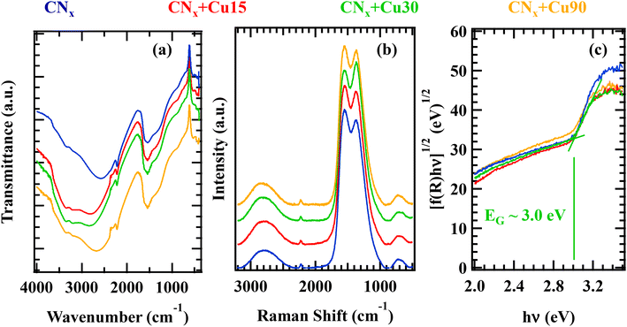 | ||
| Fig. 2 (a) FT-IR spectra, (b) Raman spectra, and (c) Tauc plots (obtained from the optical spectra in Fig. S2†) of the target specimens. | ||
The Raman spectra (Fig. 2b) were characterized by a broad signal centred at ≈700 cm−1, corresponding to the in-plane bending mode of C–N–C groups,13 the typical D and G bands of graphite-like systems located at 1372 and 1550 cm−1, respectively, a well-defined peak at 2220 cm−1 arising from C![[triple bond, length as m-dash]](https://www.rsc.org/images/entities/char_e002.gif) N stretching vibrations, and a broad band at ≈2800 cm−1 deriving from different contributions, among which C–H stretching.62 In the case of CNx + Cu30, the slightly higher intensity of the D vs. G band compared to the other specimens might be tentatively traced back to a more disordered carbon nitride structure. As described below, such an effect could originate from the enhanced dispersion of copper-containing species in the CNx + Cu30 sample. As previously reported,13,19 an increase of the system defect content can improve the separation of photogenerated holes and electrons, thus improving the system's functional behaviour. For all the target specimens, an estimation of the system's absorption edge from optical analyses (Fig. 2c; see also Fig. S2† and related comments) yielded a value of ≈3.0 eV.
N stretching vibrations, and a broad band at ≈2800 cm−1 deriving from different contributions, among which C–H stretching.62 In the case of CNx + Cu30, the slightly higher intensity of the D vs. G band compared to the other specimens might be tentatively traced back to a more disordered carbon nitride structure. As described below, such an effect could originate from the enhanced dispersion of copper-containing species in the CNx + Cu30 sample. As previously reported,13,19 an increase of the system defect content can improve the separation of photogenerated holes and electrons, thus improving the system's functional behaviour. For all the target specimens, an estimation of the system's absorption edge from optical analyses (Fig. 2c; see also Fig. S2† and related comments) yielded a value of ≈3.0 eV.
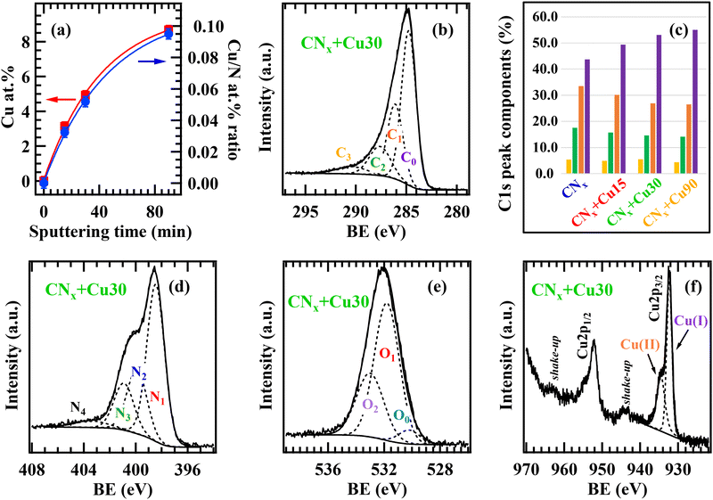
The sample's surface composition as a function of the adopted processing conditions was characterized by XPS. The survey spectra and compositional data (see Fig. S3, Table S1† and related observations) highlighted the formation of carbon-rich CNx-based materials (mean C content ≈67.5 ± 1.2 at%), with the N concentration decreasing from 26.7 to 19.7 at% upon going from CNx to CNx + Cu90, attributable to preferential nitrogen removal occurring during the subsequent RF-sputtering of copper. The bare CNx sample also contained non-negligible O amounts, which further increased upon functionalization with copper, due to Cu oxidation to Cu(I)/Cu(II) species (see below). Interestingly, the data displayed in Fig. 3a highlighted the possibility of carefully tailoring both the deposited copper amount and the related extent of CNx surface coverage.
Important information on the different C, N, and O chemical environments was obtained by peak deconvolution. Regarding the C 1s photopeak (Fig. 3b and Fig. S4a, b†), the main C0 band at 284.8 eV was primarily attributed to graphitic-like carbon atoms,21,63,64 but resulted also from adventitious contamination.65–68 The C1 component (BE = 286.1 eV) was mainly ascribed to C atoms bonded to pyrrole- and pyridine-type N,21,63,64,69,70 though additional concurrent contributions resulted from carbon atoms bonded to nitrile and amino groups on the CNx sheet edges13 (see also the FT-IR and Raman results). The C2 component (BE = 287.6 eV) was due to C bonded to “graphitic” nitrogen, formally deriving from the substitution of a graphitic C atom by an N one.63,64,69,71 Finally, the C3 band (BE = 290.4 eV) was traced back to the contribution of C–O/C–OH species and the excitation of π electrons.21,65,67,68 Data analysis revealed a significant increase of the C0 contribution in the order of CNx → CNx + Cu15 → CNx + Cu30 → CNx + Cu90, accompanied by a decrease of C1 and C2 ones (Fig. 3c). This phenomenon was related to the preferential sputtering of nitrogen in the obtained systems, progressively more pronounced for longer Cu deposition times.
The N1s signal (Fig. 3d and Fig. S4c-d†) resulted from the contribution of four components. The most intense one (N1, BE = 398.6 eV) was attributed to pyridine-type N atoms,20,21,38,63,64,69 whereas the N2 band (BE = 400.0 eV) was ascribed to pyrrole-type nitrogen, as well as to nitrile (–C![[triple bond, length as m-dash]](https://www.rsc.org/images/entities/char_e002.gif) N) and amino (NHx, x = 1, 2) groups.20,21,38,63,64,69 The N3 contribution (BE = 401.0 eV) was traced back to graphitic nitrogen atoms,20,21,27,63,64,69 while the N4 component (BE = 403.5 eV) was related to π excitation.67,70
N) and amino (NHx, x = 1, 2) groups.20,21,38,63,64,69 The N3 contribution (BE = 401.0 eV) was traced back to graphitic nitrogen atoms,20,21,27,63,64,69 while the N4 component (BE = 403.5 eV) was related to π excitation.67,70
For bare CNx, the O 1s signal (Fig. S5a†) resulted from the contribution of –OH groups (band O1, BE = 531.8 eV) and adsorbed water (band O2, BE = 533.0 eV),21,43,65–68,70 arising from the desorption of residual water from the reaction chamber walls and from sample exposure to the atmosphere. The presence of –OH (C–OH) groups on carbon nitride can favor the binding with Cu-containing species and promote their oxidation, as better substantiated in the following.43,70 The O1s photopeaks for the CuxO-functionalized samples (Fig. 3e and Fig. S5b†) contained a contribution from CuxO lattice oxygen (O0, BE = 530.3 eV), highlighting copper oxidation.43,65,66,68 The latter was also confirmed by the analysis of Cu 2p signals (Fig. 3f and Fig. S5c†), since the two Cu 2p3/2 contributions at 932.3 and 934.5 eV, exhibiting a ≈ 2![[thin space (1/6-em)]](https://www.rsc.org/images/entities/char_2009.gif) :
:![[thin space (1/6-em)]](https://www.rsc.org/images/entities/char_2009.gif) 1 ratio irrespective of copper sputtering time, correspond to Cu2O and CuO.65,66,68 Since when Cu deposition was performed on bare FTO (FTO + Cu90, Fig. S5d†), Cu 2p analysis indicated the almost exclusive presence of Cu(I) oxide,65,68 such results suggest that the CNx matrix promoted an enhanced copper oxidation.
1 ratio irrespective of copper sputtering time, correspond to Cu2O and CuO.65,66,68 Since when Cu deposition was performed on bare FTO (FTO + Cu90, Fig. S5d†), Cu 2p analysis indicated the almost exclusive presence of Cu(I) oxide,65,68 such results suggest that the CNx matrix promoted an enhanced copper oxidation.
Complementary information on in-depth composition was obtained by SIMS analyses (Fig. 4 and Fig. S6†) that, beyond the expected Cu, O, C and N signals, revealed even the Sn one deriving from the FTO substrate. The actual tin migration into the CNx films is a beneficial effect for the target end-uses thanks to the improvement of material conductivity. C and N ionic yields displayed similar trends, indicating their common chemical origin. For all specimens, copper trends evidenced an in-depth Cu dispersion throughout the underlying carbon nitride film, highlighting an intimate CuxO/CNx contact, beneficial in view of the target applications. In addition, SIMS profiles revealed an increased Cu accumulation in the outermost system regions upon increasing copper sputtering time, along with a thickness decrease of ≈70 nm upon going from the CNx + Cu15 to CNx + Cu90 specimens (see also caption to Fig. 4). In line with the above XPS results, the latter effect is attributable to the sputtering of both carbon and nitrogen (the latter being, however, preferentially removed) from the CNx matrix during the plasma-assisted deposition of Cu-containing species.
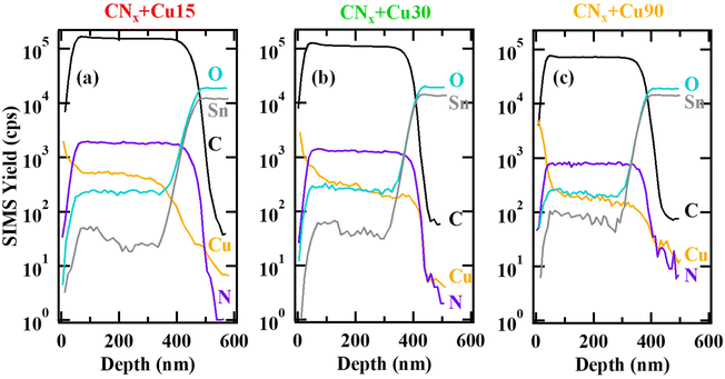 | ||
| Fig. 4 SIMS depth profiles for CNx + Cu15 (a), CNx + Cu30 (b), CNx + Cu90 (c). The deposit thickness ranged from 460 nm, for CNx + Cu15, to 370 nm, for CNx + Cu90 (uncertainty = ±30 nm). | ||
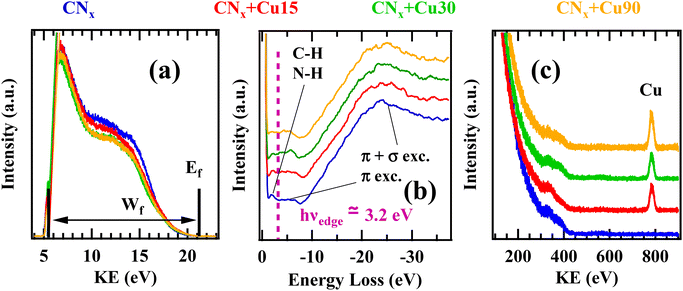
Fig. 5a displays the He(I) UPS VB for samples CNx, CNx + Cu15, CNx + Cu30 and CNx + Cu90. As a matter of fact (compare also Fig. S7†), CuxO introduction yielded a slight work function increase. REELS spectra (Fig. 5b) were characterized by two broad features due to the collective excitation of π electrons (≈5 eV) and π + σ electrons at higher energy loss (≈25 eV). All the spectra were quite similar, and only a slight decrease of the low energy feature after CuxO introduction was observed.72 The π → π* transition (at ≈5 eV) is a representative of tri-coordinated and bi-coordinated carbon and nitrogen centers, and the lack of this feature may indicate the existence of mainly tetra-coordinated C/N.72 The loss due to the presence of C–H or N–H bonds (≈2 eV) was clearly visible only for pure CNx. ISS spectra (Fig. 5c) display an intensity increase with Cu deposition time of the peak due to the scattering from copper-containing species, supporting the presence of tailored CuxO amounts on the system surface, in line with the XPS results.
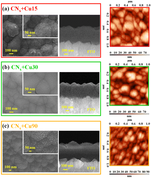
The target systems were hence analysed by FE-SEM, EDXS and AFM (Fig. 6 and Fig. S8, S9†). All deposits were very homogeneous, and featured rounded and interconnected aggregates (average dimension ≈ 150 nm). Cross-sectional images evidenced a uniform FTO coverage by relatively compact deposits. The good adhesion to the underlying FTO substrate highlighted the deposit's mechanical stability. The root-mean-square surface roughness was estimated to be ≈15 nm, regardless of the processing conditions.
To gain a deeper insight into the system nano-organization, with particular regard to the CuxO nanoaggregate size and spatial distribution as a function of preparative conditions, TEM and related analyses were carried out on the CNx + Cu15 and CNx + Cu30 samples. Both specimens presented an amorphous a-CNx layer, well adherent to the underlying FTO substrate (Fig. S10†), and an outermost Cu-rich region (Fig. S11 and S12†), thicker for CNx + Cu30 with respect to CNx + Cu15 (≈200 vs. ≈150 nm), in line with the different Cu sputtering times used for functionalizing the two samples. In both cases, EDXS chemical maps highlighted a partial superimposition of the Cu signal with C and N ones, confirming the homogeneous dispersion of copper-containing species the on and in the a-CNx matrix, and the intimate CuxO/a-CNx contact. The latter issue, in line with the above SIMS outcomes, is of key importance to profitably exploit their mutual interactions, as supported by functional tests (see below).
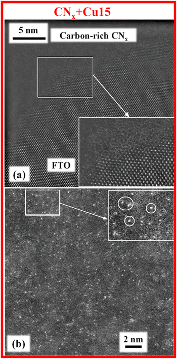
Additional important information was provided by high-resolution HAADF-STEM imaging, which evidenced in both cases the occurrence of a well-defined a-CNx/FTO interface (Fig. 7a and Fig. S10d†). Thanks to EDXS-STEM elemental mapping, it is possible to localize the copper-rich region for both samples. Since the contrast in HAADF-STEM images directly depends on the atomic number Z (≈Z2), all bright-contrast features observed in Fig. 7b and 8 could be unambiguously related to the Cu-containing species, and the data highlighted their different dimensionalities and dispersions for the target specimens. For the CNx + Cu15 sample, the apparent bright dots were indicative of ultra-dispersed, “quasi-atomic” CuxO (Fig. 7b), whose presence is an attractive issue in view of the target applications.49 Conversely, for the CNx + Cu30 specimen (Fig. 8), these species appeared to be partially combined into grouping agglomerates (mean dimensions in the range of 1.0–1.3 nm). These findings suggest the occurrence of a 3D growth mode for CuxO-containing species, with nanoaggregate growth prevailing over the initial nucleation upon increasing the copper sputtering time. As discussed below, this difference will be reflected by the material's functional performances.
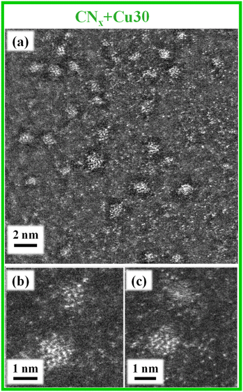 | ||
| Fig. 8 (a) Cross-sectional high-resolution HAADF-STEM image of the CNx + Cu30 sample. (b and c) Representative high-resolution HAADF-STEM images. | ||
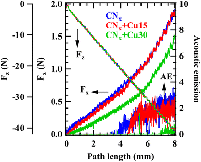
The surface mechanical properties measured by nanoindentation are summarized in Table 1. As can be observed, the hardness and the elastic modulus underwent a slight decrease with the duration of the copper sputtering treatment, i.e., upon increasing the deposited CuxO amount. The reason for this tendency lies in the surface softening effect induced by the presence of copper oxides, being softer phases than the underlying nitride film. However, the values obtained are quite near within the experimental uncertainty, revealing that the CuxO amount does not notably change the surface mechanical properties. The results from scratch tests are shown in Fig. 9, where both friction force, Fx, and acoustic emission are reported as a function of path length. Acoustic emission (AE) is defined as the elastic wave generated by the release of energy internally stored in the material structure.73 Such energy release occurs when the material undergoes changes in its internal structure, for instance due to cracking or deformation arising from an external mechanical stress. The AE signal provides information on the onset of the first cracks or an apparent change in material failure mode, in particular when clear information cannot be obtained from the friction force trend during scratch tests. To avoid incorrect interpretations, validation by electron microscopy was performed.74
| Sample | H (GPa) | E (GPa) |
|---|---|---|
| CNx | 6.3 ± 0.5 | 43 ± 5 |
| CNx + Cu15 | 5.8 ± 0.9 | 42 ± 6 |
| CNx + Cu30 | 5.5 ± 0.6 | 39 ± 5 |
Fig. 9 shows that CNx, CNx + Cu15 and CNx + Cu30 fail at an applied normal load (Fz) value of 25 N, 30 N and 32 N, respectively. These values indicate that the film as a whole is well adherent to the substrate, and can withstand a tangential force up to 25–30 N. The results show a superior adhesion to the FTO substrate for the CuxO-functionalized films, slightly increasing with the copper oxide content.
As shown in Fig. 9, the friction force is almost superimposable for the CNx and CNx + Cu15 specimens, whereas it is lower as the Cu deposition time exceeds 15 min, indicating that copper oxide introduction promotes a reduction of friction on the functionalized surface. Furthermore, the recorded critical load improves as the surface presence of copper oxides progressively increases (see also Fig. S13, S14† and related comments for further details).
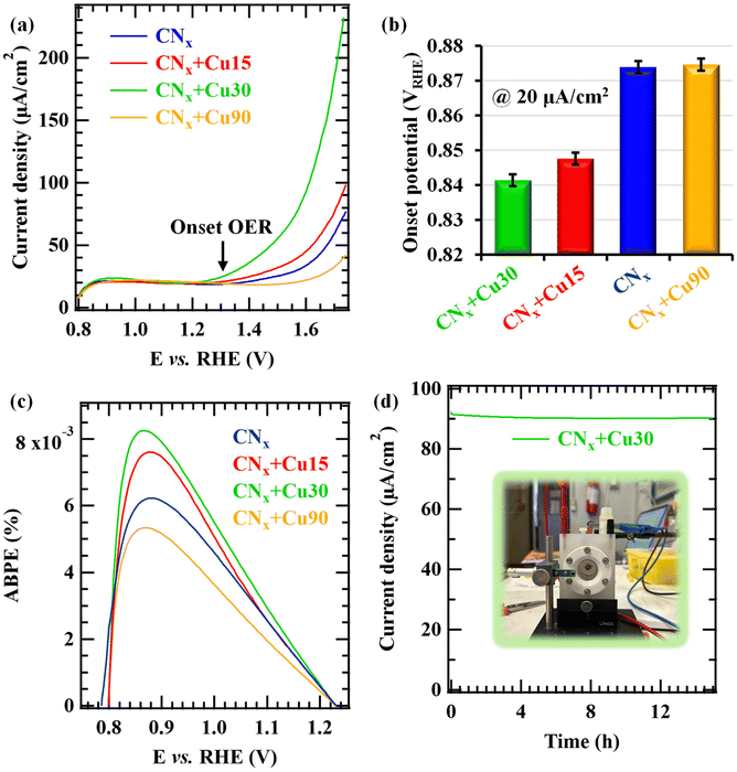
Finally, the attention was dedicated to the analysis of OER functional properties as a function of material characteristics. As a matter of fact, the evaluation of electrocatalyst's intrinsic activity would require a reliable estimation of per-site turnover frequency,75 an extremely challenging issue due to problems associated with the quantification of the inherent activity of each type of active site [Cu(I) vs. Cu(II), not to mention the synergistic CNx contribution]. As a consequence, in the following we discuss and compare the electrocatalyst's activity as a function of current densities, onset potentials, and applied bias photon-to-current efficiency (ABPE) values.
The linear sweep voltammetry (LSV) curves in Fig. 10a (compare also with Fig. S15 and S16†) provide the indication of photoelectrocatalytic activity already at ≈0.9 V vs. the reversible hydrogen electrode (RHE). This activity, comparing favourably with that of electrocatalysts based on carbon nitride and transition metal oxides (see Tables S2 and S3†), is also testified by the onset potentials measured at 0.02 mA cm−2 (Fig. 10b) and the applied bias photon-to-current efficiency (ABPE) plots (Fig. 10c). Interestingly, a steeper OER activity increase starting at ≈1.3 V vs. RHE was obtained for CNx + Cu30. It is also worth mentioning that the difference in the current densities under illumination and in the dark reaches ≈20 μA cm−2 at 1.74 V vs. RHE for the CNx + Cu30 specimen. The attractive OER onset is appreciably lower than those of similar Cu-based materials,2,76–78 and in line with the performances recently reported for CuO and CuO/CuS nanosystems.79–81 These results can be ascribed to the favourable interaction between a-CNx and CuxO. In the case of CNx + Cu30, there is an ideal compromise between the sputtered Cu amount and the ultra-dispersion of CuxO species, infiltrating into the tightly packed CNx matrix and yielding an enhanced interaction between the system components (see also the above SIMS results). Even the CNx + Cu15 specimen is characterized by a favourable OER onset, the catalytic site density is inferior to the CNx + Cu30 sample (see the above TEM analyses). At higher Cu loadings (CNx + Cu90), corresponding to larger CuxO nanoaggregates, the recorded performances are rather similar to those of bare CuxO deposited on FTO (see Fig. S15†). The present photoelectrocatalytic activity can be related to the efficient construction of p-n nano-junctions between the p-type CuxO nanoparticles and CNx, characterized by a predominantly n-type character. Under irradiation, these heterostructures promote an improved separation of photogenerated electrons and holes, as evidenced by the band diagram proposed in Fig. 11 and corroborated by the development of a photo-potential (Fig. S17†). To the best of our knowledge, the present one is the first example of heterojunctions formed between the highly disordered CNx and an ultra-dispersed oxide.
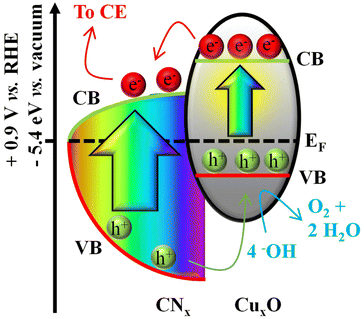 | ||
| Fig. 11 Approximate band diagram for the CNx/CuxO heterojunction. The positions of VB (valence band) and CB (conduction band) edges for a-CNx are represented by red and green curves, respectively. The VB–CB edge separation for CNx is proposed considering the EG values reported in Fig. 2. The Fermi level (EF) position on the vacuum scale was deduced from the work function values reported in Fig. S7.† | ||
To rationalize the present findings, it is worth highlighting that the dispersion of CuxO species is directly dependent on the duration of the RF-sputtering process. In particular, the results discussed so far clearly evidenced that for the CNx + Cu15 and CNx + Cu30 specimens, the lower copper oxides content in comparison with CNx + Cu90 corresponds to an enhanced CuxO dispersion both on and in a-CNx. The different CuxO amounts, dimensionalities and dispersions for the CNx + Cu15, CNx + Cu30 and CNx + Cu90 samples are thus the main characteristics responsible for the observed differences in OER performances. In particular, while the active site content increases with copper loading, p-n junction effects are indeed maximized for lower CuxO nanoaggregate dimensions. Considering all these issues, we can conclude that the best electrocatalytic activity yielded by the CNx + Cu30 specimen can be traced back to an optimal compromise between a (relatively) high density of active sites and an efficient CuxO/CNx interfacial interaction.
A key requirement for practical real-world end-uses of electrode materials is their stability under operational conditions. In this regard, Fig. 10d presents the chronoamperometric trace recorded for 15 h at 1.60 V vs. RHE and under illumination on the CNx + Cu30 sample. As can be observed, after a small decrease within the first hours, the current density remains remarkably stable up to the end of the experiment. Accordingly, LSV tests repeated after 90 and 180 days (during which the samples were stored under ambient conditions; Fig. S18†) showed negligible current density variations in comparison with the pristine measurements. The rationale for this phenomenon is the action of amorphous CNx as an efficient and stable support towards CuxO species, preventing their aggregation, preserving their dispersion, and thus accounting for the attractive system's service life. In this regard, post-operando XPS measurements confirmed that the chemical composition of the CuxO-functionalized CNx-based samples did not undergo major alterations upon electrochemical testing, as also revealed by N/C and Cu/N ratios (Fig. S19 and Table S4†). In agreement with these results, FE-SEM measurements (Fig. S20;† compared with Fig. 6b) revealed that the system morphology did not undergo any significant degradation upon operation. Taken together, such outcomes highlight how the synergistic interplay between CNx and CuxO can efficiently improve the OER photoelectrocatalytic activity of the resulting composite systems, provided that the functionalizing agent amount is judiciously optimized.
4. Conclusions
In the present study, we have developed for the first time eco-friendly CuxO/a-CNx electrocatalysts through an original multi-step plasma-assisted route. The proposed strategy consisted in the magnetron sputtering of amorphous carbon nitride films on FTO at room temperature, the subsequent introduction of very low copper amounts via RF-sputtering, and the ultimate thermal treatment under an inert atmosphere. Interestingly, controlled variations of the sole copper sputtering duration enabled tailoring of the CuxO content and dispersion in and on the carbon nitride matrix, modulating the resulting surface characteristics and the corresponding functional behavior. The improvement of OER performances, related to the formation of p–n heterojunctions efficiently suppressing charge carrier recombination, could be adjusted accordingly, as demonstrated by a comprehensive multi-technique characterization. Overall, the synthesized CuxO/a-CNx nanocomposites proved to be economically feasible and stable catalysts for the production of green hydrogen as a clean energy source, underscoring their potential in view of eventual real-world applications.Taken together, such findings contribute to the advancement of our understanding of heterojunction structures in electrocatalysts with ultra-dispersed components and their implications for WS applications. In perspective, in situ characterization techniques such as X-ray absorption fine structure (XAFS), as well as computational investigation on the target systems, could be of key importance to shed light on the process mechanism and the interplay between the chemico-physical properties of the system and the resulting functional performances. In addition, the estimation of faradaic efficiency and the evaluation of the H2 production rate are surely of great importance to gain a deeper insight into the photoelectrochemical properties of the target materials fabricated and investigated in the present work, and will be the focus of future investigations. Further attractive developments of the present research activities may also focus on optimizing the heterojunction interface and exploring other co-catalysts to enhance the system's water splitting performances.
Author contributions
Mattia Benedet: data curation, visualization, formal analysis, and writing – original draft; Angelica Fasan: investigation, data curation, and validation; Davide Barreca: supervision, funding acquisition, validation and writing; Chiara Maccato: conceptualization, validation, supervision, funding acquisition, and writing – review and editing; Cinzia Sada: formal analysis, investigation, data curation, and validation; Silvia Maria Deambrosis and Valentina Zin: validation, data curation, and writing – review and editing; Francesco Montagner: investigation and data analysis; Oleg I. Lebedev: data curation, formal analysis, and visualization; Evgeny Modin: investigation and data analysis; Gian Andrea Rizzi: formal analysis, investigation, validation, and funding acquisition; Alberto Gasparotto: data analysis, validation, formal analysis, and writing – original draft.Data availability
All the data can be found within the manuscript and ESI files.†Conflicts of interest
There are no conflicts to declare.Acknowledgements
CNR (Progetti di Ricerca @CNR – avviso 2020 – ASSIST), Padova University (PDiSC#04BIRD2020-UNIPD EUREKA, P-DiSC#02BIRD2023-UNIPD RIGENERA, DOR 2022–2024), INSTM Consortium (INSTM21PDGASPAROTTO-NANOMAT and INSTM21PDBARMAC-ATENA), and the PRIN 2022474YE8 SCI-TROPHY project (financed by the European Union – Next Generation EU – Bando PRIN 2022 – M4.C2.1.1) are acknowledged for the financial support.References
- J. Liang, J. Li, H. Dong, Z. Li, X. He, Y. Wang, Y. Yao, Y. Ren, S. Sun, Y. Luo, D. Zheng, J. Li, Q. Liu, F. Luo, T. Wu, G. Chen, X. Sun and B. Tang, Nat. Commun., 2024, 15, 6208 CrossRef CAS PubMed.
- S. M. Hosseini H, R. Siavash Moakhar, F. Soleimani, S. K. Sadrnezhaad, S. Masudy-Panah, R. Katal, A. Seza, N. Ghane and S. Ramakrishna, Appl. Surf. Sci., 2020, 530, 147271 CrossRef CAS.
- X. Zou, R. Silva, A. Goswami and T. Asefa, Appl. Surf. Sci., 2015, 357, 221–228 CrossRef CAS.
- W. Xue, W. Chang, X. Hu, J. Fan, X. Bai and E. Liu, J. Colloid Interface Sci., 2020, 576, 203–216 CrossRef CAS PubMed.
- X. Liu, Y. Han, Y. Guo, X. Zhao, D. Pan, K. Li and Z. Wen, Adv. Energy Sustainability Res., 2022, 3, 2200005 CrossRef CAS.
- Z. Li, Y. Yao, S. Sun, J. Liang, S. Hong, H. Zhang, C. Yang, X. Zhang, Z. Cai, J. Li, Y. Ren, Y. Luo, D. Zheng, X. He, Q. Liu, Y. Wang, F. Gong, X. Sun and B. Tang, Angew. Chem., Int. Ed., 2024, 63, e202316522 CrossRef CAS PubMed.
- J. Liang, Z. Cai, X. He, Y. Luo, D. Zheng, S. Sun, Q. Liu, L. Li, W. Chu, S. Alfaifi, F. Luo, Y. Yao, B. Tang and X. Sun, Chem, 2024, 10, 1–21 Search PubMed.
- H. Bae, V. Burungale, W. Na, H. Rho, S. H. Kang, S. W. Ryu and J. S. Ha, RSC Adv., 2021, 11, 16083–16089 RSC.
- A. M. Paul, A. Sajeev, R. Nivetha, K. Gothandapani, P. Bhardwaj, K. Govardhan, V. Raghavan, G. Jacob, R. Sellapan, S. K. Jeong and A. N. Grace, Diamond Relat. Mater., 2020, 107, 107899 CrossRef CAS.
- S. Zhang, J. Yan, S. Yang, Y. Xu, X. Cai, X. Li, X. Zhang, F. Peng and Y. Fang, Chin. J. Catal., 2017, 38, 365–371 CrossRef CAS.
- J. Liang, Z. Cai, Z. Li, Y. Yao, Y. Luo, S. Sun, D. Zheng, Q. Liu, X. Sun and B. Tang, Nat. Commun., 2024, 15, 2950 CrossRef CAS PubMed.
- M. Benedet, A. Gallo, C. Maccato, G. A. Rizzi, D. Barreca, O. I. Lebedev, E. Modin, R. McGlynn, D. Mariotti and A. Gasparotto, ACS Appl. Mater. Interfaces, 2023, 15, 47368–47380 CrossRef CAS.
- M. Benedet, G. A. Rizzi, A. Gasparotto, O. I. Lebedev, L. Girardi, C. Maccato and D. Barreca, Chem. Eng. J., 2022, 448, 137645 CrossRef CAS.
- H. Zhang, H. Han, X. Yang, H. Ma, Z. Song and X. Ji, Catal. Sci. Technol., 2023, 13, 6951–6958 RSC.
- N. Hussain, M. A. Abdelkareem, H. Alawadhi, A. Alaswad and E. T. Sayed, Int. J. Hydrogen Energy, 2021, 46, 6051–6060 CrossRef CAS.
- H. Shao, X. Zhang, H. Huang, K. Zhang, M. Wang, C. Zhang, Y. Yang, M. Wen and W. Zheng, ACS Appl. Mater. Interfaces, 2017, 9, 41945–41954 CrossRef CAS.
- M. Benedet, G. A. Rizzi, O. I. Lebedev, V. Roddatis, C. Sada, J.-L. Wree, A. Devi, C. Maccato, A. Gasparotto and D. Barreca, J. Mater. Chem. A, 2023, 11, 21595–21609 RSC.
- M. Fan, C. Song, T. Chen, X. Yan, D. Xu, W. Gu, W. Shi and L. Xiao, RSC Adv., 2016, 6, 34633–34640 RSC.
- M. Benedet, G. A. Rizzi, A. Gasparotto, N. Gauquelin, A. Orekhov, J. Verbeeck, C. Maccato and D. Barreca, Appl. Surf. Sci., 2023, 618, 156652 CrossRef CAS.
- I. Y. Jeon, H. J. Noh and J. B. Baek, Chem. – Asian J., 2020, 15, 2282–2293 CrossRef CAS.
- I. Bertóti, M. Mohai and K. László, Carbon, 2015, 84, 185–196 CrossRef.
- F. K. Kessler, Y. Zheng, D. Schwarz, C. Merschjann, W. Schnick, X. Wang and M. J. Bojdys, Nat. Rev. Mater., 2017, 2, 17030 CrossRef CAS.
- B. Ren, J. Huang, H. Yu, W. Yang, L. Wang, Z. Pan and L. Wang, Appl. Surf. Sci., 2016, 388, 565–570 CrossRef CAS.
- A. Fitzgerald, L. Jiang, M. Rose and T. Dines, Appl. Surf. Sci., 2001, 175, 525–530 CrossRef.
- L. Galán, I. Montero and F. Rueda, Surf. Coat. Technol., 1996, 83, 103–108 CrossRef.
- C. Wu, G. Li, X. Cao, B. Lei and X. Gao, Green Energy Environ., 2017, 2, 302–309 CrossRef.
- N. Hellgren, M. P. Johansson, E. Broitman, L. Hultman and J.-E. Sundgren, Phys. Rev. B: Condens. Matter Mater. Phys., 1999, 59, 5162 CrossRef CAS.
- F. Barreca, A. M. Mezzasalma, G. Mondio, F. Neri, S. Trusso and C. Vasi, Thin Solid Films, 2000, 377–378, 631–634 CrossRef CAS.
- M. Therasse and M. Benlahsen, Solid State Commun., 2004, 129, 139–142 CrossRef CAS.
- J. J. Li, W. T. Zheng, Z. S. Jin, T. X. Gai, G. R. Gu, H. J. Bian and C. Q. Hu, Vacuum, 2003, 72, 233–239 CrossRef CAS.
- B. Bouchet-Fabre, E. Marino, G. Lazar, K. Zellama, M. Clin, D. Ballutaud, F. Abel and C. Godet, Thin Solid Films, 2005, 482, 167–171 CrossRef CAS.
- S. Peponas, M. Guedda and M. Benlahsen, Appl. Surf. Sci., 2009, 255, 8706–8709 CrossRef CAS.
- X. Chen, J. Zhang, S. Ma, H. Hu and Z. Zhou, Acta Metall. Sin. (Engl. Lett.), 2014, 27, 31–36 CrossRef CAS.
- S. P. Lee, Sensors, 2008, 8, 1508–1518 CrossRef CAS PubMed.
- M. Aono, S. Nitta, T. Katsuno and T. Iuchi, J. Vac. Sci. Technol., B, 2000, 18, 1773–1775 CrossRef CAS.
- T. Iwasaki, M. Aono, S. Nitta, H. Habuchi, T. Itoh and S. Nonomura, Diamond Relat. Mater., 1999, 8, 440–445 CrossRef CAS.
- F. Barreca, A. M. Mezzasalma, G. Mondio, F. Neri, S. Trusso and C. Vasi, Phys. Rev. B: Condens. Matter Mater. Phys., 2000, 62, 16893–16899 CrossRef CAS.
- H.-Y. Chang and K.-Y. Lee, Jpn. J. Appl. Phys., 2015, 54, 085801 CrossRef.
- C. Spaeth, M. Kühn, F. Richter, U. Falke, M. Hietschold, R. Kilper and U. Kreissig, Diamond Relat. Mater., 1998, 7, 1727–1733 CrossRef CAS.
- J. C. Sánchez-López, C. Donnet, F. Lefèbvre, C. Fernández-Ramos and A. Fernández, J. Appl. Phys., 2001, 90, 675–681 CrossRef.
- X. C. Wang, P. Wu, Z. Q. Li, E. Y. Jiang and H. L. Bai, J. Phys. D: Appl. Phys., 2004, 37, 2127 CrossRef CAS.
- N. Kaushik, P. Sharma, M. Nishijima, A. Makino, M. Esashi and S. Tanaka, Diamond Relat. Mater., 2016, 66, 149–156 CrossRef CAS.
- M. Benedet, G. A. Rizzi, A. Gasparotto, L. Zeng, G. Pagot, E. Olsson, V. Di Noto, C. Maccato and D. Barreca, RSC Adv., 2024, 14, 7221–7228 RSC.
- Y. Tian, B. Chang, J. Fu, B. Zhou, J. Liu, F. Xi and X. Dong, J. Solid State Chem., 2014, 212, 1–6 CrossRef CAS.
- J. Chen, S. Shen, P. Guo, M. Wang, P. Wu, X. Wang and L. Guo, Appl. Catal., B, 2014, 152–153, 335–341 CrossRef CAS.
- L. Jiang, X. Yuan, Y. Pan, J. Liang, G. Zeng, Z. Wu and H. Wang, Appl. Catal., B, 2017, 217, 388–406 CrossRef CAS.
- Q. Zhang, K. Zhang, D. Xu, G. Yang, H. Huang, F. Nie, C. Liu and S. Yang, Prog. Mater. Sci., 2014, 60, 208–337 CrossRef CAS.
- I. S. Pieta, A. Rathi, P. Pieta, R. Nowakowski, M. Hołdynski, M. Pisarek, A. Kaminska, M. B. Gawande and R. Zboril, Appl. Catal., B, 2019, 244, 272–283 CrossRef CAS.
- E. Scattolin, M. Benedet, G. A. Rizzi, A. Gasparotto, O. I. Lebedev, D. Barreca and C. Maccato, ChemSusChem, 2024, e202400948 CrossRef.
- S. F. Blaskievicz, H. L. S. Santos, I. F. Teixeira, J. L. Bott-Neto, P. S. Fernández and L. H. Mascaro, Mater. Today Nano, 2022, 18, 100192 CrossRef CAS.
- C. Gao, J. Low, R. Long, T. Kong, J. Zhu and Y. Xiong, Chem. Rev., 2020, 120, 12175–12216 CrossRef CAS PubMed.
- N. Cheng, L. Zhang, K. Doyle-Davis and X. Sun, Electrochem. Energy Rev., 2019, 2, 539–573 CrossRef.
- C. V. Cushman, P. Brüner, J. Zakel, G. H. Major, B. M. Lunt, N. J. Smith, T. Grehl and M. R. Linford, Anal. Methods, 2016, 8, 3419–3439 RSC.
- S. D. Nehate, A. K. Saikumar and K. B. Sundaram, Coatings, 2021, 11, 196 CrossRef CAS.
- M. Lejeune, O. Durand-Drouhin, S. Charvet, A. Zeinert and M. Benlahsen, J. Appl. Phys., 2007, 101, 123501 CrossRef.
- X. C. Wang, Z. Q. Li, P. Wu, E. Y. Jiang and H. L. Bai, Appl. Surf. Sci., 2006, 253, 2087–2092 CrossRef CAS.
- D. Barreca, G. Carraro, D. Peeters, A. Gasparotto, C. Maccato, W. M. Kessels, V. Longo, F. Rossi, E. Bontempi and C. Sada, Chem. Vap. Deposition, 2014, 20, 313–319 CrossRef CAS.
- C. Maccato, G. Carraro, D. Peddis, G. Varvaro and D. Barreca, Appl. Surf. Sci., 2018, 427, 890–896 CrossRef CAS.
- D. Li, S. Lopez, Y. Chung, M. Wong and W. Sproul, J. Vac. Sci. Technol., A, 1995, 13, 1063–1066 CrossRef CAS.
- Y. Shao, S. Zhang, M. H. Engelhard, G. Li, G. Shao, Y. Wang, J. Liu, I. A. Aksay and Y. Lin, J. Mater. Chem., 2010, 20, 7491–7496 RSC.
- H. Wang, T. Maiyalagan and X. Wang, ACS Catal., 2012, 2, 781–794 CrossRef CAS.
- E. Liang, J. Zhang, J. Leme, C. Moura and L. Cunha, Thin Solid Films, 2004, 469, 410–415 CrossRef.
- C. Zhang, L. Fu, N. Liu, M. Liu, Y. Wang and Z. Liu, Adv. Mater., 2011, 23, 1020–1024 CrossRef CAS PubMed.
- Y.-C. Lin, C.-Y. Lin and P.-W. Chiu, Appl. Phys. Lett., 2010, 96, 133110 CrossRef.
- D. Barreca, G. Carraro and A. Gasparotto, Surf. Sci. Spectra, 2009, 16, 1–12 CrossRef CAS.
- G. Carraro, A. Gasparotto, C. Maccato, D. Peeters and D. Barreca, Surf. Sci. Spectra, 2014, 21, 1–9 CrossRef CAS.
- J. Moulder, W. Stickle, P. Sobol and D. Bomben, Handbook of X-ray photoelectron spectroscopy, Perkin-Elmer Corporation, Physical Electronics Division, Eden Prairie, MN, USA, 1992 Search PubMed.
- D. Barreca, A. Gasparotto and E. Tondello, Surf. Sci. Spectra, 2007, 14, 41–51 CrossRef CAS.
- M. Inagaki, M. Toyoda, Y. Soneda and T. Morishita, Carbon, 2018, 132, 104–140 CrossRef CAS.
- M. Benedet, A. Gasparotto, G. A. Rizzi, C. Maccato, D. Mariotti, R. McGlynn and D. Barreca, Surf. Sci. Spectra, 2023, 30, 024018 CrossRef CAS.
- Z.-H. Sheng, L. Shao, J.-J. Chen, W.-J. Bao, F.-B. Wang and X.-H. Xia, ACS Nano, 2011, 5, 4350–4358 CrossRef CAS PubMed.
- P. Prieto, C. Quiros, E. Elizalde and J. Sanz, Surf. Interface Anal., 2004, 36, 820–823 CrossRef CAS.
- D. Bahr and W. W. Gerberich, J. Mater. Res., 1998, 13, 1065–1074 CrossRef CAS.
- J. Von Stebut, F. Lapostolle, M. Bucsa and H. Vallen, Surf. Coat. Technol., 1999, 116, 160–171 CrossRef.
- N. Govindarajan, G. Kastlunger, H. H. Heenen and K. Chan, Chem. Sci., 2022, 13, 14–26 RSC.
- X. Liu, H. Zheng, Z. Sun, A. Han and P. Du, ACS Catal., 2015, 5, 1530–1538 CrossRef CAS.
- T.-T. Li, S. Cao, C. Yang, Y. Chen, X.-J. Lv and W.-F. Fu, Inorg. Chem., 2015, 54, 3061–3067 CrossRef CAS PubMed.
- X. Liu, H. Jia, Z. Sun, H. Chen, P. Xu and P. Du, Electrochem. Commun., 2014, 46, 1–4 CrossRef CAS.
- N. A. Khan, I. Ahmad, N. Rashid, S. Hussain, R. Zairov, M. Alsaiari, A. S. Alkorbi, Z. Ullah, U. Hafiz and M. F. Nazar, Int. J. Hydrogen Energy, 2023, 48, 31142–31151 CrossRef CAS.
- C. Li, S. Liu, X. Jin, Z. Zuo, H. Yang, H. Jing and X. Cao, J. Alloys Compd., 2022, 900, 163455 CrossRef CAS.
- X. Liu, S. Cui, Z. Sun, Y. Ren, X. Zhang and P. Du, J. Phys. Chem. C, 2016, 120, 831–840 CrossRef CAS.
Footnote |
| † Electronic supplementary information (ESI) available. See DOI: https://doi.org/10.1039/d4dt02186j |
| This journal is © The Royal Society of Chemistry 2024 |

