 Open Access Article
Bias switchable narrowband/broadband NIR organic photodetector fabricated with a scalable technique†
Lai-Hung
Lai
*a,
Wei-Hsiang
Lin
a,
Chin-Chuan
Hsieh
a and
Maria Antonietta
Loi
 b
b
aWafer Level Optics Organization, VisEra Technologies Company Limited, No. 12, Dusing Rd. 1 Hsinchu Science Park, Hsinchu City 30078, Taiwan. E-mail: Larry_Lai@viseratech.com
bPhotophysics and OptoElectronics, Zernike Institute for Advanced Materials University of Groningen Nijenborgh 4, 9747 AG Groningen, The Netherlands. E-mail: m.a.loi@rug.nl
First published on 11th September 2023
Abstract
Near-infrared (NIR) and shortwave infrared (SWIR) image technologies have gained significant attention for emerging applications. However, the absorption edge of Si CMOS image sensors limits their effectiveness beyond the 1000 nm wavelength range. Solution-processed organic semiconductors, with their unique photon-to-electron responses spanning from ultraviolet (UV) to the NIR/SWIR range offer exceptional versatility in optoelectronic applications. To reduce optical noise, narrow-bandpass filters are commonly employed in front of the image sensor for NIR/SWIR applications. Therefore, the development of an image sensor capable of narrowband–broadband dual-mode switchable operation holds significant convenience. In this work, we present a bias-dependent narrowband NIR organic photodiode (OPD) fabricated by blade-coating in ambient atmosphere. The OPD, featuring a 6 μm photo-active layer (PAL), exhibits narrowband photodetection with a detectivity of 1.9 × 10¹¹ Jones at a wavelength of 1100 nm under a bias of −2 V. However, when a bias exceeding −4 V is applied, it transitions into a broadband detector. Furthermore, the fabrication process for this dual-mode OPD is compatible with semiconductor foundry processes, demonstrating promise for large-scale production.
1. Introduction
Narrowband infrared photodetectors have an immense potential in 3D sensing, face recognition,1 time-of-flight sensor,2,3 and night vision,4 health monitoring,5,6 machine vision,7 optical communication,8 and spectroscopy.9 Currently, narrow band NIR/SWIR image sensor above 1000 nm are obtained by integrating a narrow-bandpass filter on an indium gallium arsenide (InGaAs) image sensor. Resulting in a bulky and extremely expensive camera, which is therefore not applicable in consumable electronics, and limiting the use of NIR/SWIR image sensors to high-end applications, such as industrial inspection and space cameras.Emerging NIR and SWIR image sensors, based on materials such as Si–Ge,10 nanocrystal quantum dot,11 and organic semiconductors12 have the potential to provide more cost-effective products compared to the one based on InGaAs. Among all, organic photodiodes (OPDs) have been demonstrated by utilizing several elegant strategies, as self-filtering narrowband photodetectors. Among these strategies are charge collection narrowing (CCN),13 charge injection narrowing (CIN),14 self-filtering,15 and microcavity enhanced narrowband OPDs.16,17 Wang18et al., demonstrated a narrowband response photomultiplication (PM) OPD based on P3HT![[thin space (1/6-em)]](https://www.rsc.org/images/entities/char_2009.gif) :
:![[thin space (1/6-em)]](https://www.rsc.org/images/entities/char_2009.gif) PC71BM (100
PC71BM (100![[thin space (1/6-em)]](https://www.rsc.org/images/entities/char_2009.gif) :
:![[thin space (1/6-em)]](https://www.rsc.org/images/entities/char_2009.gif) 1, wt/wt) with active layer deposited by drop-casting. When the active layer thickness increased to approximately 2.5 μm, the OPDs exhibited a narrowband width of full-width-at-half-maximum (FWHM) of 29 nm and an external quantum efficiency (EQE) of ∼49% at −10 V. PM was observed at −20 V with the EQE of 600% and a FWHM of 27 nm. Xie19et al., have demonstrated a self-filtering photodetector at 860, 910, and 940 nm with FWHM of around ∼50 nm, enabled by manipulation of Frenkel exciton dissociation.
1, wt/wt) with active layer deposited by drop-casting. When the active layer thickness increased to approximately 2.5 μm, the OPDs exhibited a narrowband width of full-width-at-half-maximum (FWHM) of 29 nm and an external quantum efficiency (EQE) of ∼49% at −10 V. PM was observed at −20 V with the EQE of 600% and a FWHM of 27 nm. Xie19et al., have demonstrated a self-filtering photodetector at 860, 910, and 940 nm with FWHM of around ∼50 nm, enabled by manipulation of Frenkel exciton dissociation.
However short-wave infrared imaging, is rather challenging for organic semiconductor. Recently, Kim20et al., have demonstrated a narrowband near-infrared OPD at 1040 nm exploiting intermolecular charge transfer. Siegmund16et al. achieved narrowband near-infrared photodetectors between 810 and 1550 nm using small-molecule p-type ZnPc and n-type C60 by tuning the resonant cavity thickness of the photoconductive layer, where the band gap is reduced by an intermolecular charge-transfer.
Recently, we have shown the possibility of integrating OPDs on Si wafers for the application of visible-to-infrared broadband image sensor, where the photodetector showed external quantum efficiency (EQE) of ∼50% at 940 nm, and ∼61% at 1030 nm, with a dark leakage current density of 15 nA cm−2, a bandwidth of 15 kHz at −4 V, and a dynamic range (DR) of ∼100 dB.21,22 However, additional interference-type multi-layer filters are required on the photodetectors to realize narrowband imaging. These multi-layer filters suffer from strong spectral distortion when the incident angle is larger than 30°, limiting large field of view (FOV) application, such as augmented reality (AR) and virtual reality (VR). Therefore, the fabrication complexity, film thickness, and cost of interference narrow bandpass filter limit the economical exploitation of this technology.
A new interesting strategy would be to utilize self-filtering OPD. However, there are still several challenges that need a solution before declaring as feasible the commercial exploitation of this self-filtering OPD on Si-CMOS read-out array. These challenges fall both in the domain of the performances but also on the fabrication: i) high detectivity, values in the range of 1012 Jones should be achieved; ii) low dark current (below 10−7 A cm−2); iii) fast response speed (at least 10 μs); iv) good dynamic range (minimum 60 dB), and finally to develop a scalable fabrication process compatible with CMOS foundry.23
In this work, we present a scalable and reliable way to fabricate a relatively thick and uniform active layer for narrowband photodetection with sensitivity peak at ∼1100 nm. Interestingly, when the thickness of the active layer is above 6 μm for a bias of at −2 V, a monochromatic narrowband sensitivity at 1100 nm with EQE of 25% and FWHM of 66 nm is observed. Interestingly, when the bias is larger than −4 V, the response spectrum becomes broadband. As far as we know, this is the most exceptional narrowband/broadband photodetector with bias switchability that has been reported, with an EQE exceeding 1000 nm wavelength. The optical electric field distribution inside the active layer indicates the electric field driven charge collection. At the end we demonstrate, for the first time, the application of this OPD for Si wafer inspection, offering a great prospective for a cost-effective solution for industrial applications.
2. Results and discussion
2.1 Blade coating for scalable fabrication
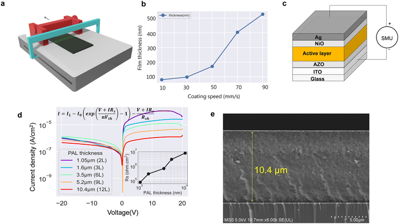
The most used technique nowadays to deposit relatively thick (order of thousands of nanometres) and homogeneous layers of organic semiconductor is spin coating.17,29 A low boiling point solvent and high concentration are necessary to achieve elevated thicknesses (above few hundreds of nanometers) with spin coating. However, spin coating is not an industrially friendly technique for scalable fabrication since it wastes ∼90% of the materials during the spinning process. Drop casting it is also not a scalable and reliable method for fabricating commercial devices as it depends on difficult to control parameters. On the contrary, blade coating (Fig. 1a) is a scalable fabrication technique closely related to industrial-level techniques such as roll-to-roll printing and slot-die printing. The thickness and morphology of the film can be controlled by the speed of the blade, the distance between the blade and substrate, the deposition temperature (controlled by the plate temperature), and the solution concentration.24 The film formation during blade-coating is related to interplay of different deposition modes. At lower blading speed, the evaporation mode, where the ink dries right after the blade moves away from the ink, dominates the film formation. While at higher blading speed, the Landau–Levich mode, where the as-coated thin ink layer is still wet right after blading, dominates the film formation. Fig. 1b shows the dry PAL film thickness as a function of the coating speed, showing that at a higher blading speed, the film becomes thicker. We performed the blade coating process several times to achieve the desired thickness of PAL, where each layer is totally dried before the coating of the next layer.2.2 Photodetector performance
In this study, we have fabricated organic photodiode (OPD) using an inverted architecture, which is depicted in Fig. 1c. The structure consists of glass/ITO/AZO/PD004![[thin space (1/6-em)]](https://www.rsc.org/images/entities/char_2009.gif) :
:![[thin space (1/6-em)]](https://www.rsc.org/images/entities/char_2009.gif) PD-A2/HTL/Ag. To fabricate the active layer, a commercially available ink named PD004
PD-A2/HTL/Ag. To fabricate the active layer, a commercially available ink named PD004![[thin space (1/6-em)]](https://www.rsc.org/images/entities/char_2009.gif) :
:![[thin space (1/6-em)]](https://www.rsc.org/images/entities/char_2009.gif) PD-A2 was utilized. This ink formulation satisfies the requirements of industrial applications and is composed of a halogen-free solvent used to dissolve both an electron-donating polymer and electron-accepting small molecule.
PD-A2 was utilized. This ink formulation satisfies the requirements of industrial applications and is composed of a halogen-free solvent used to dissolve both an electron-donating polymer and electron-accepting small molecule.
The UV-vis spectra of pure PD004 and PD-A2 films are shown in Fig. S1a.† PD004 possesses a wide bandgap, allowing efficient absorption of ultraviolet and visible light. While, PD-A2, is characterized by a narrow bandgap, primarily absorbing near-infrared radiation.
The energy-level diagram of the photoactive materials is presented in Fig. S1b,† showing the optimal band structure of the PD004![[thin space (1/6-em)]](https://www.rsc.org/images/entities/char_2009.gif) :
:![[thin space (1/6-em)]](https://www.rsc.org/images/entities/char_2009.gif) PD-A2 bulk heterojunction (BHJ) film, which facilitates the efficient separation and collection of charge carriers.
PD-A2 bulk heterojunction (BHJ) film, which facilitates the efficient separation and collection of charge carriers.
The dark JV measurements obtained from devices with varied blade coating PAL thickness are shown in Fig. 1d. The organic active layer is blade coated several times at 70 °C to reach a relatively thick layer while maintaining a good uniformity (Fig. 1e). The dark current measurements are analysed by fitting them with the current–voltage equation below.
 | (1) |
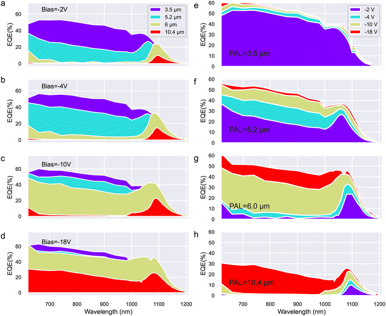
Fig. 2 show the EQE spectra of the photodiodes, all of them show a broadband sensitivity from 600 to 1200 nm. Therefore, our broadband OPDs has a NIR sensitivity that is ∼100 nm longer than the state-of-the-art Si image sensor Nyxel-2 (Fig. S3†).25 The EQE spectra show tunability when the PAL thickness is varied above a critical thickness of 5.2 μm. We observed that the OPDs with a PAL thickness of 6 μm (Fig. 2g) has a narrowband peak at 1100 nm with a FWHM of 66 nm. Interestingly, when a bias above −4 V is applied to photodiodes with a PAL thickness of 6 μm, the spectrum becomes broadband. This switchable width of the detection spectrum offers significant potential for imaging application.
Lan et al.,26 have reported near-infrared and visible light dual-mode OPDs by trap-assisted charge injection at the organic/cathode interface, where the dual-mode is switched by applying forward bias or reverse bias. However, in a real application, when integrating an OPDs and three transistors (1D3T) in an active pixel architecture or capacitive transimpedance amplifier (CTIA) pixel architecture, the photodiode should only work under reverse bias. Here, we demonstrate the possibility of dual-mode OPDs by controlling the reverse bias voltage, which is more practical when integrating them into CMOS readout circuit.
To understand the working principle of our dual-mode switchable photodetectors, we look into the details of the photon to electron conversion process. The EQE of our OPDs are governed by three main processes: i) incident light absorbed by the photoactive layer creates excitons; 2) exciton dissociation into free carriers (electrons/holes) at donor–acceptor interfaces; 3) free carriers (electron/hole) transport towards electrodes and collection by electrodes; 4) trapping of charge carriers.
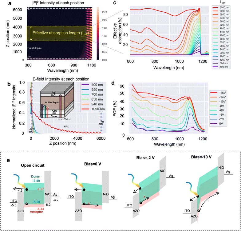
The distribution of incident light absorbed by the photoactive layer can be simulated by the transfer matrix method (Fig. 3a and b), where we found that a photon with a 940 nm wavelength has the shortest penetration depth of ∼300 nm. In contrast, the photons with 1100 nm can penetrate into the device's rear side due to its low absorption coefficient at the band edge. The narrowband EQE can be explained by the charge collection narrowing (CCN) effect, where the carriers generated in the front side of our device architecture are holes and are not able to be collected by the rear electrode since the PAL thickness is larger than the carrier diffusion length. While above 1000 nm wavelength, photon-generated carriers are equally distributed along the device thickness (Fig. 3a), and therefore can be easily collected by the electrode. When applying a high bias, two mechanisms are possible. First, the hole accumulated near the front side bends the energy diagram severely, allowing the hole to be directly injected from the external circuits, similar to a photo-switch under strong bias.17 The other possibility is that the strong electric field inside the PAL drifts the hole from the front side to the rear side. If the first mechanism dominates, the device may show an EQE higher than 100%, which should also happen in thinner PAL devices. However, we observe that the EQE saturates at voltages above −14 V. Therefore, we ascribe the bias-dependent EQE to a better charge collection under a strong electric field.
In Fig. 3a and b, the optical field distributions inside the device consisting of ITO (110 nm)/AZO (20 nm)/PAL (6 μm)/NiO (40 nm)/Ag (100 nm) show that photons with wavelengths smaller than 1000 nm hardly penetrate into the device's rear side due to the relatively large absorption coefficient (Fig. S4†). The fringes originating from the interference between incident light and reflected light from the Ag electrode gradually become apparent when incident light wavelengths exceed 1000 nm. We further calculated the effective absorption spectra in the middle of the PAL from 400–6000 nm (Fig. 3c). The effective absorption spectrum is defined as the spectrum measured from photon-generated electrons that can be collected by the external circuit. The photon-generated electrons inside the effective absorption length (Leff) can be collected, while for the one outside the Leff charge collection by the electrodes is not possible. In the middle at 5200 nm, the effective spectra show narrowband absorption characteristics. In comparison, the effective absorption spectra become broadband when the effective thickness is above 5200 nm, meaning that charges generated on the front side starts to contribute to the photocurrent. Fig. 3d shows the bias-dependent EQE spectra, which resembles the effective absorption spectra shown in Fig. 3c, showing that the electric field drifts the charge carriers generated on the front side and enhances the charge collection efficiency.
When the Leff is larger than the PAL thickness (Leff > L), the photocurrent follows the eqn (2).
| Jsatph = qgL | (2) |
 | (3) |
The charge generation rate displays a spatial distribution variation at different wavelengths (Fig. 3a and b). At a shorter wavelength, the charge generation is located near the front side, while NIR photons are distributed more uniformly inside the device. Therefore, at short wavelength, the carriers need longer Leff in order to be collected by the electrode. Thanks to the original spatial charge generation variation along different wavelengths, the short wavelength follows eqn (3). In contrast, the NIR wavelength follows eqn (2).
The effective absorption length (Leff) is related to the carrier mobility, the carrier lifetime, and the electric field (Leff = μhτhE), which can be enhanced by applying a bias. Once Leff approaches L by applying a high bias, at short wavelength illumination, the photocurrent follows eqn (2) instead of eqn (3).
The energy diagram in Fig. 3e, depicts the mechanism for different wavelengths that we have described above.
The responsivity (R) and detectivity (D*) of our devices were calculated using eqn (4) and (5):
 | (4) |
 | (5) |
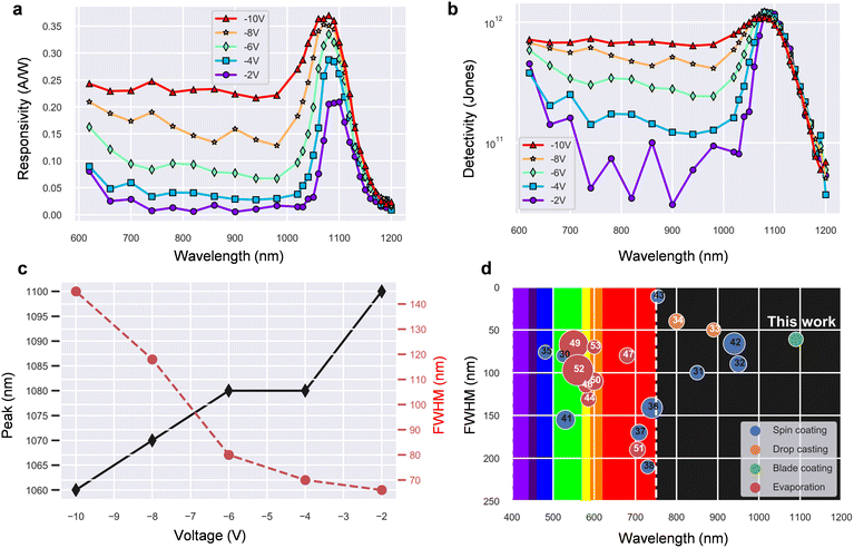 | ||
| Fig. 4 a. Responsivity; b. detectivity and c. peak wavelength and corresponding FWHM at various biases. d. FWHM–wavelength plot for organic narrowband photodetector reported in the literature (the size of the circle indicates the relative detectivity value). See Table S3.†30–54 | ||
To calculate the detectivity, we need to measure the noise current. A photodiode's dominant noise source is the shot noise due to dark currents. Flicker noise can become somewhat significant when the integration time is very long. Assuming that the device performance is shot noise limited,27 the detectivity is calculated to be 1.2 × 10¹² Jones at λ of 1100 nm using the responsivities mentioned above and dark current densities at a certain bias (Table S2†) from eqn (5). This detectivity value is already comparable to commercially available InGaAs photodetectors (D* ∼ 1012 Jones at a wavelength of 1000 nm, Hamamatsu G10899), even in the absence of additional enhancements such as microlenses or anti-reflection coatings. The full width at half maximum (FWHM) of the photodetector response is 66 nm. Here we noted that eqn (5) neglects the influence of the flicker noise (1/f-noise) and the thermal noise on the total noise current of the photodetectors.28,29 When considering these factors, the detectivity is expressed as  , where R is responsivity, A is the device area, and Sn is the noise spectral density. Fig. S5† shows the detectivity of the photodetector with a PAL of 6 μm reaches 1.9 × 10¹¹ Jones at 1100 nm wavelength at low operation voltage (−2 V). Which is almost 1 order of magnitude below the estimation performed with the approximate formula.
Fig. 4c shows peak wavelength and corresponding FWHM at various biases, with FWHM increasing from 66 nm to 80 nm when the voltage increased from −2 V to −6 V; however, meanwhile the peak wavelength is slightly shifting from 1100 nm to 1080 nm. This is caused by the fact that photons with longer wavelength can penetrate deeper into the device, and only those photo-electrons can reach the electrode under low bias condition.
Fig. 4d shows the detectivity and FWHM–wavelength plot for the most advanced organic narrowband photodetector reported in literature. When compare to these body of work, appears clear that our work is a breakthrough in terms of IR detection wavelength and narrow FWHM, furthermore our devices are unique as they are the only one fabricated with a scalable process.
2.3 Response time of the OPD
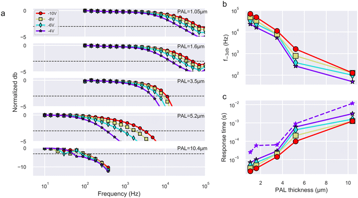
The response time of the photodetector can be characterized by measuring their 3 dB bandwidth (Fig. 5a).22 This measurements where performed at 520 nm by illuminating the photodetector with a fast response LED and putting a circuit in series with the OPD with a 50-ohm shunt resistance whose voltage drop is measured by a lock-in amplifier. After scanning from 10 Hz to 100![[thin space (1/6-em)]](https://www.rsc.org/images/entities/char_2009.gif) 000 kHz, the voltage values read from the lock-in amplifier are normalized to their maximum. We defined the frequency corresponding to a −3 dB decay of the signal as f−3dB (Fig. 5b). Finally, Fig. 5c shows the signal response time calculated using eqn (6).55–57
000 kHz, the voltage values read from the lock-in amplifier are normalized to their maximum. We defined the frequency corresponding to a −3 dB decay of the signal as f−3dB (Fig. 5b). Finally, Fig. 5c shows the signal response time calculated using eqn (6).55–57 | (6) |
As expected, the response time of the photodetector increases as the thickness of the PAL increases (Fig. 5c), varying from 6.8 × 10⁻⁶ s to 3.2 × 10⁻³ s when the thickness increases from 1.05 to 10.4 μm. In fact, the response time is affected by transit time and RC delay, as shown in eqn (7).
 | (7) |
We further performed impedance spectroscopy on the OPDs to analyze the carrier transport kinetics under illumination. First, the sample is measured under 520 nm LED illumination at various reverse DC biases with the addition of small AC signal perturbation. Nyquist plots shown in Fig. S6† were fitted using the equivalent circuit model following a previous report, and the relevant data are summarized in Tables S4 and S5.† In the equivalent circuit, R1/C1 are related to the bulk, R2/C2 to the interface, and R3 to the series resistance. From all the impedance fitting result, we obtained that the bulk resistance increases from 104 ohms to 106 ohms for the OPD device, with thicknesses increasing from 1.05 to 10.4 μm at 0 V and −4 V under green light illumination, which is consistent with the series resistance from the dark IV-curve fitting (Fig. S2f†). The average carrier transit time of the bulk (τbulk) of the equivalent circuit was calculated using:58
| τbulk = Rbulk × Cbulk | (8) |
The response time obtained by impedance fitting measured at −4 V is plotted as a dashed line in Fig. 5c, where the RC time increases 473 times when the PAL thickness increases from 1.05 to 10.4 μm, indicating the same behavior observed in the frequency domain measurement. As a result, the photon-to-electron response time is dominated by the RC time, which should be faster when the pixel size becomes smaller (the current pixel size is 2320 μm and device area is ∼0.054 cm2).
2.4 Linear dynamic range of the OPD
The linear dynamic range (LDR) is another important characteristic for an image sensor, which is defined as the ratio between the maximum achievable signals that a photodetector can quantitatively detect divided by the photodiode noise, following eqn (9).59 | (9) |
 and
and  are the maximum and minimum values of detectable photocurrent and incident light intensity, respectively.20,21
The current vs. light intensity relations are shown in Fig. 6 for various PAL thicknesses (1.05, 3.5, and 6 μm). The dynamic range of the OPD is larger than 112 dB. The photodetector with PAL thickness of 1.05 and 3.5 μm shows a single slope of 1.024 and 1.054, respectively. However, samples of 3.5 μm thickness are showing some saturation for light intensity superior to 10 mW cm−2. The current vs. light intensity plot shows two distinct slopes for the photodetector with a PAL thickness of 6 μm. When the light intensity is weaker than 0.1 mW cm−2, the slope is close to 0.846; while the slope becomes 0.277 when the light intensity is higher than 0.1 mW cm−2, which is ascribed to strong carrier recombination under elevated light intensity. This phenomenon is interesting in terms of system-level dynamic range for the CMOS image sensor, since the full-well capacity of the pixel is determined by the photocurrent density and capacitance of the pixel (ΔQ = CΔV = iΔt, where Q is the charge held, V is the electrical potential, i is the current, t is the time). Therefore, the pixel is more difficult to saturate for the device with smaller slope dynamic range under strong light condition.
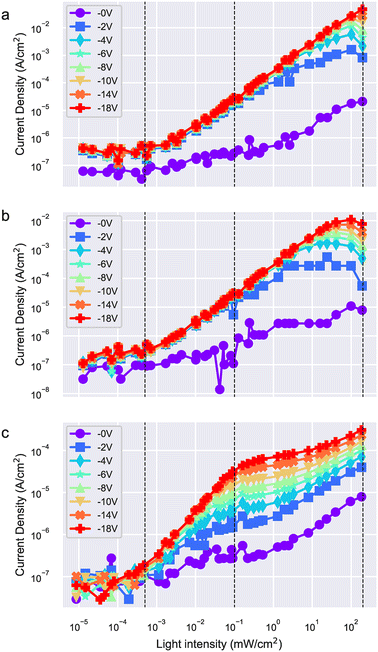 | ||
| Fig. 6 Linear dynamic range of the photodetector with PAL thickness of: a. 1.05 μm, b. 3.5 μm, and c. 6 μm measured at 808 nm. | ||
2.5 Imaging of the NIR narrowband OPD beyond Si
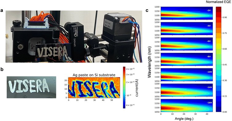
The sensitivity of our OPDs can reach wavelengths of 1200 nm allowing us to realize a system for the infrared inspection of Si wafer with a thickness of 700 μm, whose bandgap is 1.12 eV (1071 nm). Fig. S7a shows the setup for the Si wafer inspection. We wrote “VISERA” on the Si wafer with silver paste and placed it on the x–z two-axis motor stage (Fig. 7a). A monochromatic light at 1100 nm wavelength was focused on the sample, with a spot size was ∼1 × 2 mm. The OPD is placed in front of the Si sample to inspect. The measurement is done in transmission mode by moving the Si wafer line by line (raster-scanning). The signal point by point is measured by a lock-in amplifier and converted into images by a computer. Fig. 7b shows the measured sample (left) and transmission image (right) obtained from the OPD. The slight distortion of the transmission image is caused by the vibration of the step motor during the measurement. Therefore, we demonstrated that our photodetector or better an image sensor fabricated with it can be used for Si wafer inspection and can become a cost-effective replacement for InGaAs image sensor.2.6 Angular-dependent narrowband property
An ideal narrowband photodetector should have little angular-dependent peak shifting. The angular-dependent property of our photodetector is investigated by the setup shown in Fig. S7b.† The resulting measurements on our photodetector showing a weak angle-dependent blue shift are reported in Fig. 7c. For non-normal incidence, even though the optical field distribution inside the device changes, the propagation wavelength to the device's rear side does not change. It is interesting to note that generally cavity-based narrowband photodetectors suffer of a strong angle-dependent behaviour, where the resonance wavelength decreases for non-normal excitation, with the peak position following a parabolic dispersion, leading to a reduction in resonance wavelength of more than 50 nm for angles above 45°.163. Conclusion
In summary, we demonstrate the scalable fabrication of a dual-mode narrowband–broadband switchable photodetector with low operation voltage. Multi layers can be deposited by blade coating, allowing reaching thicknesses above 10 μm. These photodetectors show a narrowband photodetection at 1100 nm with a detectivity of 1.9 × 10¹¹ Jones and a FWHM of 66 nm at a bias of −2 V; while the detectivity spectrum becomes broadband when the bias is larger than −4 V. The photo-response time of the device is ∼10−4 s, corresponding to ∼1 kHz bandwidth, which is already fast enough for the fabrication of a common anode global shutter image sensor. The photon-to-electron response time is dominated by the RC time, showing that the detector should be faster when the pixel size becomes smaller. The dual-slope of the photodetector with a thickness above 6 μm provides designers with a further handle to extend the image sensor's dynamic range. In addition, the narrowband peak position is invariant for the light incident angle allowing for high field of view imaging.4. Experimental section/methods
4.1 Materials
The photo-active layer in this study consists of a blend of two components: a conjugated polymer donor called PD004 and a non-fullerene acceptor named PD-A2. PD004 was synthesized by modifying a commercially available donor polymer to enhance its solubility and energy levels, specifically for applications in organic photodiodes (OPDs). On the other hand, PD-A2 was designed by incorporating long alkyl side chains, a ladder-type core, and a fluorinated end group into its molecular structure using non halogenated solvents. Some information about the development of these materials is available in the following patents.60,61 The organic molecules used in the experiment were obtained from Raynergy Tek corporation, while the AZO/NiO nanoparticle dispersions were purchased from Avantama AG. Other chemicals and solvents utilized in this research were acquired from the Sigma-Aldrich Chemical Corporation.4.2 Sample preparation
In sequence, the lithographically patterned ITO/glass substrates are washed with soap, acetone, and DI water for 10 min. AZO, PD004![[thin space (1/6-em)]](https://www.rsc.org/images/entities/char_2009.gif) :
:![[thin space (1/6-em)]](https://www.rsc.org/images/entities/char_2009.gif) PD-A2, and NiO are deposited in ambient atmosphere, where AZO and NiO are deposited by a spin coating, while a blade coating process is used to deposits the donor accept blend of commercial name PD004
PD-A2, and NiO are deposited in ambient atmosphere, where AZO and NiO are deposited by a spin coating, while a blade coating process is used to deposits the donor accept blend of commercial name PD004![[thin space (1/6-em)]](https://www.rsc.org/images/entities/char_2009.gif) :
:![[thin space (1/6-em)]](https://www.rsc.org/images/entities/char_2009.gif) PD-A2. The blade coating of the PAL is done on a self-built blade coater composed of a commercial blade, a step motor, a hotplate, and a microcontroller. Finally, thermal evaporation is used to deposits the Ag cathode through a shadow mask which defines the electrode.
PD-A2. The blade coating of the PAL is done on a self-built blade coater composed of a commercial blade, a step motor, a hotplate, and a microcontroller. Finally, thermal evaporation is used to deposits the Ag cathode through a shadow mask which defines the electrode.
4.3 Characterization
J–V characteristics of the devices were acquired using a Keithley 2400 source measurement unit. The EQE spectrum was measured by a self-built EQE system shown in Fig. S7b.† The monochromatic light intensity is calibrated by Si (818-UV) and Ge (818-IR) reference cells. The film thickness of each layer was determined by SEM technique (Hitachi SU8220) in a cross-sectional view and operated at 5 kV. A sputtered Pt film covered the samples to increase the conductivity of the sample surface for SEM measurement. The carrier response time and dynamic range were measured using a self-built optical system, where the 520 nm LED is used as a light source for carrier response time measurement. Electrochemical impedance spectroscopy (EIS) measurements were performed by CHI 600E series electrochemical analyzer/workstation under 520 nm LED illumination with an intensity of 4.09 mW cm−2 while applying a DC bias voltage equal to 0 V and −4 V, respectively, with a 50 mV AC signal perturbation at a frequency ranging from 1 MHz to 1 Hz. The linear dynamic range was measured under various light intensities controlled by self-built motorized ND filters. The 808 nm laser coupled with a diffuser and a collimator is applied as a light source for LDR measurement. The demo of the Si wafer inspection is performed under 1100 nm wavelength, where the Si sample is placed on the self-built 2-axis stage composed of two step motors controlled by a microcontroller. The transmission signals are collected by our photodetector. The optical simulations are based on the transfer matrix method (TMM).62 All data and figures are manipulated by python.Conflicts of interest
The authors declare no competing financial interest.Acknowledgements
The authors express their gratitude for the research funds provided by VisEra Technologies Company Limited. Furthermore, the authors extend their appreciation to Prof. Chih-Shan Tan and Y.-M. Chang for their valuable support during the experiments. The authors also acknowledge Kelly Shih and Ives Chang for their insightful discussions.Notes and references
- S. Z. Li, R. F. Chu, S. C. Liao and L. Zhang, IEEE Trans. Pattern Anal. Mach. Intell., 2007, 29, 4 Search PubMed.
- M. H. Conde, T. Kerstein, B. Buxbaum and O. Loffeld, 2020 IEEE SENSORS, 2020 Search PubMed.
- S. Lee, K. Yasutomi, M. Morita, H. Kawanishi and S. Kawahito, Sensors, 2020, 20(1), 116 CrossRef.
- Y. Wang, B. Siegmund, Z. Tang, Z. Ma, J. Kublitski, S. Xing, V. C. Nikolis, S. Ullbrich, Y. Li, J. Benduhn, D. Spoltore, K. Vandewal and K. Leo, Adv. Opt. Mater., 2020, 9(6), 2001784 CrossRef.
- C. M. Lochner, Y. Khan, A. Pierre and A. C. Arias, Nat. Commun., 2014, 5, 5745 CrossRef CAS PubMed.
- Y. Khan, D. Han, A. Pierre, J. Ting, X. Wang, C. M. Lochner, G. Bovo, N. Yaacobi-Gross, C. Newsome, R. Wilson and A. C. Arias, Proc. Natl. Acad. Sci. U. S. A., 2018, 115(47), E11015 CrossRef CAS.
- G. Simone, D. Di Carlo Rasi, X. de Vries, G. H. L. Heintges, S. C. J. Meskers, R. A. J. Janssen and G. H. Gelinck, Adv. Mater., 2018, 30, 1804678 CrossRef.
- J. Clark and G. Lanzani, Nat. Photonics, 2010, 4, 438 CrossRef CAS.
- Z. Tang, Z. Ma, A. Sanchez-Diaz, S. Ullbrich, Y. Liu, B. Siegmund, A. Mischok, K. Leo, M. Campoy-Quiles, W. Li and K. Vandewal, Adv. Mater., 2017, 29, 1702184 CrossRef.
- C.-L. Chen, S.-W. Chu, B.-J. Chen, Y.-F. Lyu, K.-C. Hsu, C.-F. Liang, S.-S. Su, M.-J. Yang, C.-Y. Chen, S.-L. Cheng, H.-D. Liu, C.-T. Lin, K. P. Petrov, H.-W. Chen, K.-C. Chu, P.-T. Huang, P.-C. Wu, N. Na and S.-L. Chen, 2020 IEEE International Solid- State Circuits Conference - (ISSCC), DOI:10.1109/ISSCC19947.2020.9063107.
- V. Pejović, E. Georgitzikis, J. Lee, I. Lieberman, D. Cheyns, P. Heremans and P. E. Malinowski, IEEE Trans. Electron Devices, 2022, 69(6), 2840–2850 Search PubMed.
- H. Shekhar, A. Fenigstein, T. Leitner, B. Lavi, D. Veinger and N. Tessler, Sci. Rep., 2020, 10, 7594 CrossRef CAS PubMed.
- A. Armin, R. D. J. Vuuren, N. Kopidakis, P. L. Burn and P. Meredith, Nat. Commun., 2015, 6, 6343 CrossRef CAS PubMed.
- W. Wang, M. Du, M. Zhang, J. Miao, Y. Fang and F. Zhang, Adv. Opt. Mater., 2018, 6, 1800249 CrossRef.
- B. Xie, R. Xie, K. Zhang, Q. Yin, Z. Hu, G. Yu, F. Huang and Y. Cao, Nat. Commun., 2020, 11, 2871 CrossRef CAS PubMed.
- B. Siegmund, A. Mischok, J. Benduhn, O. Zeika, S. Ullbrich, F. Nehm, M. Böhm, D. Spoltore, H. Fröb, C. Körner, K. Leo and K. Vandewal, Nat. Commun., 2017, 8, 15421 CrossRef CAS PubMed.
- Z. Zhao, C. Xu, Y. Ma, K. Yang, M. Liu, X. Zhu, Z. Zhou, L. Shen, G. Yuan and F. Zhang, Adv. Funct. Mater., 2022, 2203606 CrossRef CAS.
- W. Wang, F. Zhang, M. Du, L. Li, M. Zhang, K. Wang, Y. Wang, B. Hu, Y. Fang and J. Huang, Nano Lett., 2017, 17(3), 1995–2002 CrossRef CAS PubMed.
- B. Xie, R. Xie, K. Zhang, Q. Yin, Z. Hu, G. Yu, F. Huang and Y. Cao, Nat. Commun., 2020, 11, 2871 CrossRef CAS.
- J. H. Kim, A. Liess, M. Stolte, A. M. Krause, V. Stepanenko, C. Zhong, D. Bialas, F. Spano and F. Würthner, Adv. Funct. Mater., 2021, 33, 2100582 CAS.
- J. L. Wu, L. H. Lai, Y. T. Hsiao, K. W. Tsai, C. M. Yang, Z. W. Sun, J. C. Hsieh and Y. M. Chang, Adv. Opt. Mater., 2021, 10, 2101723 CrossRef.
- L. H. Lai, C. C. Hsieh, J. L. Wu and Y. M. Chang, ACS Appl. Electron. Mater., 2022, 4(1), 168–176 CrossRef CAS.
- Y. Wang, J. Kublitski, S. Xing, F. Dollinger, D. Spoltore, J. Benduhn and K. Leo, J. Mater. Chem. C, 2022, 9, 220–251 CAS.
- N. Sukharevska, D. Bederak, V. M. Goossens, J. Momand, H. Duim, D. N. Dirin, M. V. Kovalenko, B. J. Kooi and M. A. Loi, ACS Appl. Mater. Interfaces, 2021, 13(4), 5195–5207 CrossRef CAS PubMed.
- https://www.ovt.com/purecel-pixel-tech/nyxel-technology-generation-2 .
- Z. Lan, Y. Lei, W. K. E. Chan, S. Chen, D. Luo and F. Zhu, Sci. Adv., 2020, 6, eaaw8065 CrossRef CAS.
- N. Gasparini, A. Gregori, M. Salvador, M. Biele, A. Wadsworth, S. Tedde, D. Baran, I. McCulloch and C. J. Brabec, Adv. Mater. Technol., 2018, 1800104 CrossRef.
- N. Gasparini, A. Gregori, M. Salvador, M. Biele, A. Wadsworth, S. Tedde, D. Baran, I. McCulloch and C. J. Brabec, Adv. Mater. Technol., 2018, 3(7), 1800104 CrossRef.
- A. Armin, R. D. Jansen-Van Vuuren, N. Kopidakis, P. L. Burn and P. Meredith, Nat. Commun., 2015, 6, 6343 CrossRef CAS.
- R. D. Jansen-Van Vuuren, A. Pivrikas, A. K. Pandey and P. L. Burn, J. Mater. Chem. C, 2013, 1, 3532–3543 RSC.
- D. M. Lyons, A. Armin, M. Stolterfoht, R. C. R. Nagiri, R. D. Jansen-Van Vuuren, B. N. Pal, P. L. Burn, S. C. Lo and P. Meredith, Org. Electron., 2014, 15, 2903–2911 CrossRef CAS.
- H. Zhang, S. Jenatsch, J. De Jonghe, F. Nuësch, R. Steim, A. C. Véron and R. Hany, Sci. Rep., 2015, 5, 9439 CrossRef CAS PubMed.
- A. Armin, R. D. J. Vuuren, N. Kopidakis, P. L. Burn and P. Meredith, Nat. Commun., 2015, 6, 6343 CrossRef CAS.
- L. Shen, Y. Zhang, Y. Bai, X. Zheng, Q. Wang and J. Huang, Nanoscale, 2016, 8, 12990 RSC.
- J. Miao, F. Zhang, M. Du, W. Wang and Y. Fang, Adv. Opt. Mater., 2018, 6, 1800001 CrossRef.
- A. Liess, A. Arjona-Esteban, A. Kudzus, J. Albert, A. M. Krause, A. Lv, M. Stolte, K. Meerholz and F. Würthner, Adv. Funct. Mater., 2019, 29, 1805058 CrossRef CAS.
- K. Xia, Y. Li, Y. Wang, L. Portilla and V. Pecunia, Adv. Opt. Mater., 2020, 8, 1902056 CrossRef CAS.
- S. Z. Hassan, H. J. Cheon, C. Choi, S. Yoon, M. Kang, J. Cho, Y. H. Jang, S. K. Kwon, D. S. Chung and Y. H. Kim, ACS Appl. Mater. Interfaces, 2019, 11, 28106–28114 CrossRef CAS.
- H. Opoku, B. Lim, E. S. Shin, H. Kong, J. M. Park, C. Bathula and Y. Y. Noh, Macromol. Chem. Phys., 2019, 220, 1900287 CrossRef.
- J. Kim, S. Yoon, K. M. Sim and D. S. Chung, J. Mater. Chem. C, 2019, 7, 4770 RSC.
- J. Y. Kim, P. Vincent, J. Jang, M. S. Jang, M. Choi, J. H. Bae, C. Lee and H. Kim, J. Alloys Compd., 2020, 813, 152202 CrossRef CAS.
- J. Kang, J. Kim, H. Ham, H. Ahn, S. Y. Lim, H. M. Kim, I. N. Kang and I. H. Jung, Adv. Opt. Mater., 2020, 8, 2001038 CrossRef.
- B. Xie, R. Xie, K. Zhang, Q. Yin, Z. Hu, G. Yu, F. Huang and Y. Cao, Nat. Commun., 2020, 11, 2871 CrossRef CAS PubMed.
- T. Schembri, J. H. Kim, A. Liess, V. Stepanenko, M. Stolte and F. Würthner, Adv. Opt. Mater., 2021, 9, 2100213 CrossRef CAS.
- K. H. Lee, D. S. Leem, J. S. Castrucci, K. B. Park, X. Bulliard, K. S. Kim, Y. W. Jin, S. Lee, T. P. Bender and S. Y. Park, ACS Appl. Mater. Interfaces, 2013, 5, 13089–13095 CrossRef CAS PubMed.
- H. O. Toshikatsu Sakai, H. Seo and T. Takagi, MRS Adv., 2015, 1, 459–464 CrossRef.
- S. J. Lim, D. S. Leem, K. B. Park, K. S. Kim, S. Sul, K. Na, G. H. Lee, C. J. Heo, K. H. Lee, X. Bulliard, R. I. Satoh, T. Yagi, T. Ro, D. Im, J. Jung, M. Lee, T. Y. Lee, M. G. Han, Y. W. Jin and S. Lee, Sci. Rep., 2015, 5, 7708 CrossRef CAS PubMed.
- W. Li, D. Li, G. Dong, L. Duan, J. Sun, D. Zhang and L. Wang, Laser Photonics Rev., 2016, 10, 473–480 CrossRef CAS.
- W. Li, S. Li, L. Duan, H. Chen, L. Wang, G. Dong and Z. Xu, Org. Electron., 2016, 37, 346–351 CrossRef CAS.
- M. G. Han, K. B. Park, X. Bulliard, G. H. Lee, S. Yun, D. S. Leem, C. J. Heo, T. Yagi, R. Sakurai, T. Ro, S. J. Lim, S. Sul, K. Na, J. Ahn, Y. W. Jin and S. Lee, ACS Appl. Mater. Interfaces, 2016, 8, 26143–26151 CrossRef CAS.
- W. Li, H. Guo, Z. Wang and G. Dong, J. Phys. Chem. C, 2017, 121, 15333–15338 CrossRef CAS.
- C. W. Joo, J. Kim, J. Moon, K. M. Lee, J. E. Pi, S. Y. Kang, S. D. Ahn, Y. S. Park and D. S. Chung, Org. Electron., 2019, 70, 101–106 CrossRef CAS.
- G. H. Lee, X. Bulliard, S. Yun, D.-S. Leem, K.-B. Park, K.-H. Lee, C.-J. Heo, I.-S. Jung, J.-H. Kim, Y. S. Choi, S.-J. Lim and Y. W. Jin, Opt. Express, 2019, 27, 25410–25419 CrossRef CAS PubMed.
- D. Shen, Z. Guan, M. Li, S.-W. Tsang, W. Zhang, M.-F. Lo and C.-S. Lee, J. Mater. Chem. C, 2021, 9, 3814 RSC.
- Z. Zhao, C. Xu, L. Niu, X. Zhang and F. Zhang, Laser Photonics Rev., 2020, 14, 2000262 CrossRef CAS.
- K. Yang, Z. Zhao, M. Liu, L. Niu, X. Zhao, G. Yuan, X. Ma and F. Zhang, J. Mater. Chem. C, 2022, 10, 10888–10894 RSC.
- M. Liu, Q. Fan, K. Yang, Z. Zhao, X. Zhao, Z. Zhou, J. Zhang, F. Lin, A. K.-Y. Jen and F. Zhang, Sci. China: Chem., 2022, 65, 1642 CrossRef CAS.
- S. Braun, W. R. Salaneck and M. Fahlman, Adv. Mater., 2009, 21, 1450–1472 CrossRef CAS.
- Z. Zhao, M. Liu, K. Yang, C. Xu, Y. Guan, X. Ma, J. Wang and F. Zhang, Adv. Funct. Mater., 2021, 31(43), 2106009 CrossRef CAS.
- Z. Zhu, H. Pan, M. Dress, S. Lu and A. Facchetti, US8772442, 2013.
- G. Morse, L. Nanson, W. Mitchell, M. Krompiec, M. D'Lavari and A. Pron, US10991893, 2017.
- P. Yeh, Optical Waves in Layered Media, Wiley, 2005 Search PubMed.
Footnote |
| † Electronic supplementary information (ESI) available: UV-vis spectra and energy-level diagram of the photoactive material, dark I–V curve fitting, summary of the photodetector performance, impedance fitting, comparison between the state-of-the art Si CMOS image sensors with OPD, and summary of narrowband OPD performance from literatures. See DOI: https://doi.org/10.1039/d3lf00089c |
| This journal is © The Royal Society of Chemistry 2024 |

