
 Open Access Article
 This Open Access Article is licensed under a Creative Commons Attribution-Non Commercial 3.0 Unported Licence
Improved transparency and conductivity in copper chromium oxide coatings through aliovalent doping and stoichiometry control†
Jaewon
Kim
*ab,
Owen
Kendall
b,
Triet Thien Huu
Nguyen
b,
Joel
van Embden
b and
Enrico
Della Gaspera
 *b
*b
aAgency for Science, Technology and Research, Institute of Materials Research and Engineering, 2 Fusionopolis Way, Singapore 138634, Singapore. E-mail: jaewon_kim@imre.a-star.edu.sg
bSchool of Science, RMIT University, Melbourne, VIC 3000, Australia. E-mail: enrico.dellagaspera@rmit.edu.au
First published on 9th February 2024
Abstract
Copper delafossites are well known p-type oxide semiconductors with transparent conducting properties, displaying high electrical conductivity, optical transparency, and wide band gap (∼3 eV), and as such they have potential applications in various optoelectronic devices. However, their performance is still inferior compared to their n-type counterparts. In this study, we investigate the deposition of delafossite copper chromium oxide (CuCrO2) thin films employing a sol–gel precursor solution in conjunction with ultrasonic spray pyrolysis. Our research focuses on assessing the influence of magnesium doping on the structural, electrical, and optical properties of the CuCrO2 coatings. We employ a range of characterization techniques, including X-ray diffraction, X-ray photoelectron spectroscopy, scanning electron microscopy, electrical conductivity, and optical spectroscopy. Continuous, dense and polycrystalline thin films of phase pure delafossite films are obtained across all conditions, regardless of the addition of Mg dopants. A copper-poor precursor formulation was chosen to enhance the visible transparency of the coatings. Importantly, the electrical properties of CuCrO2 thin films exhibit substantial enhancement following the introduction of Mg. Our optimized films exhibit conductivity of 52.8 S cm−1, visible transmittance greater than 50%, and an optical band gap of approximately 3 eV. These noteworthy findings constitute as a promising foundation for the development of high-performance p-type transparent conductors.
Introduction
Transparent conductive oxides (TCOs) are key components of many optoelectronic devices, including solar cells, photodetectors, light emitting diodes, electrochromics and touchscreen displays, due to their dual property of being highly optically transparent in the visible region, and also electrically conductive. The vast majority of TCOs are based on wide band gap n-type semiconductors such as indium oxide (In2O3), zinc oxide (ZnO) and tin dioxide (SnO2), which are usually appropriately doped with aliovalent ions to increase their n-type character and their electrical conductivity.1–5 These materials have shown high transparency (>85% transmittance across the visible range, due to their band gap being in the ultraviolet region, above ∼3 eV) and high electrical conductivity (up to 104 S cm−1).6,7 However, while n-type TCOs are well established and developed, there is a lack of high-performance p-type TCO due to their inferior electrical properties and pronounced absorption across the visible spectrum.8–10 This has drastically limited the fabrication of all-oxide devices, power electronics and optoelectronics with innovative architectures, which all require stable, highly conductive, and highly transparent p-type TCO.Copper-based ternary oxides, and especially copper delafossites, constitute a class of materials that has shown great promise as p-type TCOs compared to other traditional p-type oxides.11–17 They have a general formula of CuMO2 where M is a trivalent cation (Al, Cr, Fe, or Ga).11,18–20 Their wide band gap and enhanced conductivity due to their distinctive valence band structure make them highly suitable for p-type TCO.21 In addition to their fundamental properties, copper delafossites can be aliovalently doped to increase their p-type character, mostly using divalent cations such as zinc, magnesium and nickel to replace the native trivalent ion (chromium, gallium or aluminium).22–30 Moreover, being delafossites ternary oxides, they possess two cation sites and their electrical and optical properties can be further modified and adapted by changing their stoichiometry (i.e. synthesizing Cu-poor or Cu-rich compositions).31,32
Amongst all delafossites, CuCrO2 is particularly attractive because of its proven excellent optoelectronic properties, that surpass those of other delafossites, especially as far as electrical conductivity is concerned. For such reason, CuCrO2 thin films have been explored using a variety of deposition techniques such as sputtering,26 pulsed laser deposition (PLD),33 atomic layer deposition (ALD),34 chemical vapor deposition (CVD),29 spin-coating,24 and spray pyrolysis.35 In our previous work, we presented a thorough investigation on the fabrication of CuCrO2 thin films using ultrasonic spray pyrolysis, through the analysis of both solution chemistry and deposition parameters.17 A careful selection of decomposition temperature, film thickness and copper to chromium ratio enabled to produce films with high electrical conductivity and reasonable transparency. In terms of electrical and optical properties, these films were on par or better than any other delafossite thin films in the literature, with the exception a few examples were the CuCrO2 films were fabricated by vacuum depositions. Importantly, we discovered that samples fabricated from stoichiometric (Cu![[thin space (1/6-em)]](https://www.rsc.org/images/entities/char_2009.gif) :Cr = 1:1) precursor solutions were copper rich, and that reducing the amount of copper precursor resulted in coatings with higher visible transparency, which however came at the cost of a reduced electrical conductivity. In this study, we expand on these results, showing the incorporation of Mg dopant in these CuCrO2 thin films prepared ultrasonic spray pyrolysis using a simple alcohol-based sol–gel precursor solution. Improved visible transparency (up to 60% average transmittance across the visible range) while maintaining high electrical conductivity (>50 S cm−1) was simultaneously achieved balancing both the dopant amount and the Cu:Cr ratio, providing access to improved transparent electrode performances. Our study suggests a simple and versatile fabrication method for an attractive material candidate for transparent electronic devices that require high-performance p-type TCOs.
:Cr = 1:1) precursor solutions were copper rich, and that reducing the amount of copper precursor resulted in coatings with higher visible transparency, which however came at the cost of a reduced electrical conductivity. In this study, we expand on these results, showing the incorporation of Mg dopant in these CuCrO2 thin films prepared ultrasonic spray pyrolysis using a simple alcohol-based sol–gel precursor solution. Improved visible transparency (up to 60% average transmittance across the visible range) while maintaining high electrical conductivity (>50 S cm−1) was simultaneously achieved balancing both the dopant amount and the Cu:Cr ratio, providing access to improved transparent electrode performances. Our study suggests a simple and versatile fabrication method for an attractive material candidate for transparent electronic devices that require high-performance p-type TCOs.
Experimental
Materials
Copper(II) acetylacetonate (Cu(acac)2, 99.9%) and chromium(III) acetylacetonate (Cr(acac)3, 99.7%) were purchased by Sigma-Aldrich. Magnesium(II) acetylacetonate (Mg(acac)2, 98%) was purchased from STREM Chemicals. Methanol, acetone, and isopropanol (IPA) were obtained from Univar. All chemicals were used without further purification.Film deposition
A precursor solution consisting of 8 mM of Cu(II), 12 mM of (Cr(III) + Mg(II) acetylacetonate), in methanol was prepared and stirred for 2 h. For example, in a typical reaction for a sample of nominal composition [Cu0.4Cr0.6−xMgxO]2 where x = 0.1, 251.3 mg Cu(acac)2, 452.7 mg, Cr(acac)3, and 32.0 mg Mg(acac)2 were dissolved in 120 mL methanol. Substrates (borosilicate glass and silicon) were ultrasonically cleaned in acetone and IPA for 10 minutes each, and then dried with a nitrogen stream. Deposition of doped and undoped CuCrO2 films via spray pyrolysis was carried out with a Nadetech ND-SP ultrasonic spray coater equipped with a 120 kHz nozzle. The deposition temperature was fixed at 450 °C. The details of the spray pyrolysis parameters can be found in our earlier work.17 In the following, the samples will be labelled with the nominal composition based on precursor amount, according to the simplified notation: [CuaCrb−xMgxO]2, where a + b = 1, and 0 ≤ x ≤ 0.12. However the true experimental composition obtained via compositional analysis is also provided.Characterization techniques
X-ray diffraction (XRD) patterns for CuCrO2 films were obtained with a Bruker D4 diffractometer operating at 40 kV and 35 mA using Cu Kα radiation (1.5418 Å). The surface morphology and thickness of CuCrO2 films were measured by field emission scanning electron microscopy (FE-SEM, FEI Verios 460). Compositional analysis via energy-dispersive X-ray spectroscopy (EDX) was conducted within the same instrument. X-ray photoelectron spectroscopy (XPS) was conducted with a Kratos AXIS Supra X-ray photoelectron spectrometer equipped with a monochromated Al Kα X-ray source (1486.7 eV) and a concentric hemispheric electron analyzer. Sheet resistance measurements in 4-point probe configuration were measured by a Jandel multi height probe combined with an RM3000 test unit. The sheet resistance was always measured in the center, and multiple samples prepared in the same way were measured and the results presented as an average value. Optical transmittance and reflectance spectra were acquired with an Agilent Cary 5000 spectrophotometer equipped with an integrating sphere, which enabled us to acquire the total values (diffuse + direct) of both transmittance and reflectance. Optical measurements were conducted in the center of each sample used for sheet resistance measurements.Results and discussion
Mg-doped CuCrO2 thin films were coated on borosilicate substrates via a sol–gel process, using methanol as the solvent due to its ability to readily dissolve all precursors. Ultrasonic spray pyrolysis was used as the deposition technique because it can readily produce high quality, crystalline oxide coatings, and also provide a mean to achieve tuneable doping concentration by simple modification of the precursor concentration.6 We have recently showed excellent p-type CuCrO2 coatings by ultrasonic spray pyrolysis, through a careful optimisation of deposition temperature, and precursor type and concentration.17 Here, we build on these results and demonstrate the incorporation of Mg dopants into compositionally adjusted CuCrO2 coatings to produce p-type transparent conductors with greatly improved optoelectronic properties and related figure of merit. The ultrasonic spray pyrolysis system is schematically presented in Fig. 1a. Briefly, the sol–gel precursor solution is fed through an ultrasonic nozzle via a syringe pump to ensure constant flowrate. The ultrasonic nozzle atomizes the liquid into small, monodisperse droplets that are ejected from the nozzle and directed onto the heated sample using a nitrogen stream to shape the precursor mist. | ||
| Fig. 1 a) Schematic illustration of the ultrasonic spray pyrolysis system. b) XRD patterns for the prepared CuCrO2 thin film at various Mg concentrations. The expected peak positions for delafossite CuCrO2 according to ICDD No. 74-0983 are reported at the bottom. c) Schematic representation of the CuCrO2 lattice. | ||
As mentioned earlier, we chose a precursor formulation deficient in copper (nominal Cu:Cr = 0.4:0.6) to avoid the formation of copper-rich films, and deposited coatings with varying Mg amounts, by replacing different amounts of Cr with suitable amounts of Mg, in order to keep Mg + Cr constant, according to a nominal composition [Cu0.4Cr0.6−xMgxO]2, where x varies between 0 and 0.12. We used energy dispersive X-ray spectroscopy (EDX) to quantify the amount of dopant incorporated within the films, and the true Cu:Cr ratio. As shown in Fig. S1 and Table S1,† the samples prepared from a copper deficient solution have a Cu:Cr ratio ∼1:1, while samples deposited from a 1:1 molar mixture of Cu and Cr precursors are heavily copper rich. This greatly impacts their optical and electrical properties (vide infra). The presence of Mg is also demonstrated, and its amount is seen to increase linearly with the amount of precursor used. However, the experimentally detected Mg amount is ∼25% of the amount of precursor used.
X-ray diffraction (XRD) was used to confirm the crystallinity of the deposited coatings. All samples display the (101) and (012) diffraction peaks of rhombohedral delafossite CuCrO2 (space group R![[3 with combining macron]](https://www.rsc.org/images/entities/char_0033_0304.gif) m, ICDD No. 74-0983), with no additional peaks detected, confirming phase purity and the absence of impurity phases such as MgO, within the detection limits of the XRD (Fig. 1b). Importantly, while the presence of additional phases cannot be completely excluded since they might be either amorphous, or not resolved by XRD, we performed a simple test by spraying the Mg precursor alone at 450 °C. The resulting sample was amorphous, confirming that this pyrolysis temperature is sufficient to decompose the dopant precursor, but not to crystallize MgO itself. The absence of nominally high intensity diffraction peaks such as (006), (104) and (018) suggest strong texturing of the deposited films, which is also consistent with the literature.26,27,34,36
m, ICDD No. 74-0983), with no additional peaks detected, confirming phase purity and the absence of impurity phases such as MgO, within the detection limits of the XRD (Fig. 1b). Importantly, while the presence of additional phases cannot be completely excluded since they might be either amorphous, or not resolved by XRD, we performed a simple test by spraying the Mg precursor alone at 450 °C. The resulting sample was amorphous, confirming that this pyrolysis temperature is sufficient to decompose the dopant precursor, but not to crystallize MgO itself. The absence of nominally high intensity diffraction peaks such as (006), (104) and (018) suggest strong texturing of the deposited films, which is also consistent with the literature.26,27,34,36
Careful analysis of the (012) peak shows a progressive shift in diffraction angle as a function of Mg amount, consistent with incorporation of extrinsic dopants within the CuCrO2 crystal (Fig. S2†). However, this shift points to a reduction in the lattice spacing, which is counterintuitive since Mg2+ has a larger ionic radius than Cr3+. The reason behind this unusual behavior is still under investigation. Mg doping was also found to have a minor effect on the overall crystallinity of the CuCrO2 coatings. In fact, with the increase in Mg amount, and especially at high concentration, the diffraction peaks are slightly broadened and reduced in intensity. However, the films remain crystalline.
The surface morphology of the films was investigated using SEM. Continuous, pinhole-free films with polydisperse grains (size of the order of 40–80 nm) were observed for all compositions, except at Mg nominal amount exceeding 0.1, where the grain size was negatively affected (Fig. 2 and S3 in ESI†). This is consistent with the XRD results which showed a reduced crystallinity at high Mg loading. The loss in deposition quality is also accompanied by a reduced thickness measured at high concentrations, while the thickness remains rather constant in samples prepared from lower Mg amount (Fig. 2d and S4†). As mentioned, most samples show a rather broad grain size distribution, with a few larger grains being observed over a dense layer of smaller grains. This is consistent with our earlier results on undoped CuCrO2.17
 | ||
| Fig. 2 SEM images for CuCrO2 films deposited with different nominal Mg concentrations. a) 0 b) 0.05, c) 0.10. The scale bar is 400 nm and is common to all SEM images. d) Plot of film thickness for various Mg concentrations. | ||
We used XPS to analyze the chemical composition and chemical environments of the prepared films, and a typical survey spectrum is shown in Fig. S5.† The high resolution XPS spectra of the main regions of interest are reported in Fig. 3. Fig. 3a shows the Cu 2p region, with the Cu 2p3/2 and Cu 2p1/2 main components, centered at ∼932.2 eV and ∼952.0 (spin–orbit splitting of ∼19.8 eV), indicative of Cu+, as expected from delafossite materials. However, the presence of Cu2+ is also observed, due to the shoulder peaks at ∼934 eV and 954 eV, and the corresponding satellite (shake-up) peaks at higher binding energies, characteristic of Cu(II) species. This is not surprising, since surface oxidation of Cu species in delafossite is known, and it is consistent with our earlier work17 and also other literature reports.31,37,38 Importantly, negligible differences are observed in the copper environment as a function of Mg doping.
 | ||
| Fig. 3 XPS characterization for CuCrO2 films as a function of Mg concentration. a) Cu 2p, b) Cr 2p, c) O 1s, and d) C 1s and Mg KLL. The inset in (d) shows a zoomed view of the Mg KLL region. | ||
Fig. 3b presents the Cr 2p region, showing the two main components Cr 2p3/2 and Cr 2p1/2 centered at 576.0 eV and 585.8 eV respectively (spin–orbit splitting: ∼9.8 eV), which are a clear indication of chromium in the +3 oxidation state as expected in delafossites.17,31,37 The third peak in this region is a copper Auger peak (Cu LMM, ∼569.5 eV). The only difference observed in this region is the intensity ratio between the Cr 2p and the Cu LMM component, with the chromium peaks becoming slightly less intense compared to the copper peak at higher Mg doping. This is not surprising, since when doping with magnesium, a certain fraction of the Cr precursor was substituted with the Mg precursor, resulting in an overall lower Cr amount. Fig. 3c shows the O 1s region, with its typical asymmetric line shape: the main component at low binding energies (∼529.8 eV) corresponds to oxygen in a metal oxide environment (lattice oxygens), while the shoulder at higher binding energies is due to a series of contributions including surface hydroxides, and adsorbed organics containing C–O and C![[double bond, length as m-dash]](https://www.rsc.org/images/entities/char_e001.gif) O groups. Again, no difference in the oxygen environment is observed across the samples prepared in this study. The detailed XPS fittings for Cu 2p, Cr 2p and O 1s are presented in Fig. S6.† Analysis of the Mg signal was quite challenging, since we could not detect clearly its presence in the conventional Mg 1s region (expected peak at ∼1305 eV). However, clear signature from Mg appears in the Mg KLL Auger region (300–310 eV), with a single peak centered at ∼305 eV, indicative of Mg2+ in an oxide environment, as shown in Fig. 3d.39 The intensity of this peak is also clearly increasing with the amount of Mg precursor used for the films deposition. The presence of Mg at least in the samples with the highest doping levels can also be inferred from the analysis of the Mg 2p region (Fig. S7a†), which is also quite close to the Cr 3p region. However, due to the low intensity of these peaks, only a shoulder can be seen here. The reason for the lack of Mg 1s peak could be that Mg is located just underneath the sample surface, and this effect could be enhanced by the presence of surface adventitious carbon. However, due to differences in kinetic energy, the Auger signal can be detected even if the Mg 1s is not. XPS analysis after etching could be a solution, however it was decided to avoid this process since even the mildest etching has been shown to heavily affect the copper environment in CuCrO2-based films.17 In addition to the elements and their oxidation state, XPS also provides information on their electronic properties via analysis of the valence band region. In fact, the onset of the valence band spectrum corresponds to the energy difference between the valence band maximum and the Fermi energy. All samples show a Fermi energy very close, if not within the valence band edge, confirming a strong p-type character of the prepared delafossite films (Fig. S7b†).
O groups. Again, no difference in the oxygen environment is observed across the samples prepared in this study. The detailed XPS fittings for Cu 2p, Cr 2p and O 1s are presented in Fig. S6.† Analysis of the Mg signal was quite challenging, since we could not detect clearly its presence in the conventional Mg 1s region (expected peak at ∼1305 eV). However, clear signature from Mg appears in the Mg KLL Auger region (300–310 eV), with a single peak centered at ∼305 eV, indicative of Mg2+ in an oxide environment, as shown in Fig. 3d.39 The intensity of this peak is also clearly increasing with the amount of Mg precursor used for the films deposition. The presence of Mg at least in the samples with the highest doping levels can also be inferred from the analysis of the Mg 2p region (Fig. S7a†), which is also quite close to the Cr 3p region. However, due to the low intensity of these peaks, only a shoulder can be seen here. The reason for the lack of Mg 1s peak could be that Mg is located just underneath the sample surface, and this effect could be enhanced by the presence of surface adventitious carbon. However, due to differences in kinetic energy, the Auger signal can be detected even if the Mg 1s is not. XPS analysis after etching could be a solution, however it was decided to avoid this process since even the mildest etching has been shown to heavily affect the copper environment in CuCrO2-based films.17 In addition to the elements and their oxidation state, XPS also provides information on their electronic properties via analysis of the valence band region. In fact, the onset of the valence band spectrum corresponds to the energy difference between the valence band maximum and the Fermi energy. All samples show a Fermi energy very close, if not within the valence band edge, confirming a strong p-type character of the prepared delafossite films (Fig. S7b†).
The key aspect of this work is the investigation of the optical and electrical properties of the prepared films. Fig. 4, S8 and S9† present an overview of the optical properties for these coatings, showing a high transparency in the visible range (51–61%) for all Mg compositions. This is due to the selected copper-deficient precursor formulation, that enables lower visible absorption compared to films produced with a 1:1 Cu:Cr precursor ratio, which show an average visible transmittance of only ∼34% due to a much larger absorptance at visible wavelengths (46% for [Cu0.5Cr0.5O]2vs. 34% for [Cu0.4Cr0.6O]2, Fig. S9†). In addition, working in Cu-poor conditions makes the formation of Cu2O and CuO phases unfavourable, therefore avoiding strong absorption in the visible associated with these impurity phases.
 | ||
| Fig. 4 Optical properties of CuCrO2 films at various Mg concentration. a) Transmittance spectra. The dashed line is the spectrum for a conventional, copper-rich film. b) Photograph of samples. c) Tauc plots, and d) the estimated band gap. | ||
There doesn't seem to be a clear trend in transmittance with Mg doping, besides a slight increase on average compared to the undoped sample. This is consistent with literature, which shows that reducing the amount of Cr3+via substitution with Mg2+ (or Al3+) can help reducing visible absorptions.18,40 Moreover, it has also been reported that Mg2+ suppresses the nucleation of the aforementioned copper oxide phases during deposition, further contributing to reduce unwanted visible absorptions.41,42
Visually, the samples display a slight greenish/purplish tinge, which is due to a combination of absorption and reflection at slightly different wavelengths (interference fringes arising from different thickness/refractive index combinations, see Fig. 4b and S10†). Importantly, the calculated band gap for all films remains reasonably constant at ∼3 eV regardless of Mg amount, except for large doping levels. However, in these conditions structural and morphological changes were observed (reduced crystallinity, smaller grain size) so the slight widening of the band gap cannot be ascribed to the presence of Mg alone. The lack of the expected Burstein–Moss effect with Mg doping can be explained by noting that the undoped CuCrO2 is already a degenerate semiconductor with a large hole density exceeding 1021 cm−3.
After discussing the optical properties, we now move to analyse the electrical properties. Fig. 5 shows the sheet resistance value and the conductivity of CuCrO2 coatings prepared in this study as a function of the amount of Mg. The sheet resistance is seen to gradually decrease by almost an order of magnitude with increasing the amount of Mg up to x ∼ 0.1. Concurrently, the electrical conductivity – calculated from the sheet resistance and the sample thickness – increases steadily over the same doping range. This is due to aliovalent p-doping provided by Mg2+ substituting Cr3+ in the delafossite lattice, therefore increasing the overall hole concentration. A similar trend has been reported previously in a other studies of Mg-doped copper oxides and copper delafossites.30,36,40,41
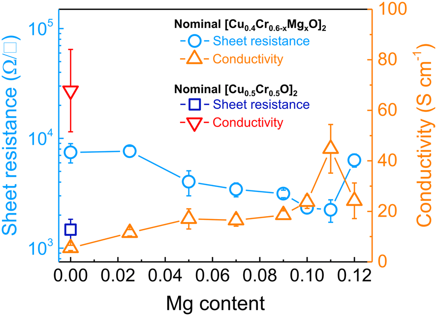 | ||
| Fig. 5 Electrical properties of CuCrO2 films as a function of Mg amount. The values for the copper rich, undoped CuCrO2 prepared from stoichiometric precursors are also reported. | ||
The highest conductivity (44.8 ± 9.6 S cm−1 on average, with 52.8 S cm−1 as the record value) was obtained for a nominal Mg doping level x = 0.11, while the undoped sample displayed a much lower value of 5.5 ± 1.0 S cm−1 on average, with 6.4 as the record value. This change in electrical properties is due to aliovalent doping provided by magnesium ions. Mg2+ can substitute Cr3+, generating an excess of positively charged holes, and therefore enhancing the p-type character of CuCrO2. We note that the undoped CuCrO2 prepared from stoichiometric precursors (resulting in copper-rich coatings) has a higher electrical conductivity (67.8 ± 16.3 S cm−1), due to its higher copper content that increases its p-type conductivity.17 However, as mentioned above, more copper in CuCrO2 films leads to a decrease in visible optical transmittance, negatively affecting the performance of transparent electrodes, exemplified by the figures of merit discussed in the following. Developing a copper poor precursor formulation, which results in stoichiometric, compositionally balanced films, and introducing Mg as aliovalent dopant enables to retain high conductivity similar to that of copper rich coatings, and gain enhanced transparency, therefore boosting the overall TCO performances.
The quality of a transparent electrode is usually assessed through a combination of optical transparency in the wavelength range of interest, and electrical conductivity. These two parameters are conventionally combined in various figures of merit (FoM), the two most common being Haacke's and Gordon's. The Haacke's FoM43 is defined as the transmittance of the film raised to the tenth power, and divided by its sheet resistance, as follow:

On the other hand, Gordon's FoM1 is defined as the ratio between the electrical conductivity and the absorption coefficient in the visible region:

The two FoM for the samples prepared in this study are presented in Fig. 6. The values have been measured for multiple samples and the data are presented as an average value (with associated error), and also highlighting the best value for each. There isn't a clear trend in Haackes' FoM with Mg doping, besides an initial increase compared to the undoped sample. This is not unexpected considering the optical and electrical properties of these samples, which all show comparable transmittance when in copper deficient formulations. Importantly, the undoped sample has already a highly improved FoM compared to the “standard” CuCrO2 deposited from 1:1 Cu:Cr precursors, due to its lower Cu amount, and these two factors combined provide ∼2 orders of magnitude increase in FoM from <2 × 10⁻⁸ (Ω sq−1) to >1 × 10⁻⁶ (Ω sq−1). If we consider the Gordon's FoM, we can appreciate its strong dependence on the electrical properties: the steady rise in conductivity observed as a function of Mg doping is reflected in a constant increase in FoM. Importantly, the best samples prepared in this study not only have a massively improved Haacke's FoM compared to conventional, copper-rich coatings, but also supersede them when comparing the Gordon's FoM. In fact, the average value of the standard sample is ∼1 mS (best is 1.45 mS), while for our optimised formulation (optimised Cu:Cr and optimised Mg doping) the average FoM is ∼1.35 mS, with best value >1.7 mS. These are some of the highest values ever reported for delafossite oxides, and are only surpassed by coatings deposited with complex, slow and expensive vacuum based depositions such as ALD and sputtering.30,44 This is exemplified in Fig. 7, where the average visible transmittance and electrical conductivity are plotted for the samples presented here and compared with other copper delafossite transparent electrodes (CuCrO2, and CuGaO2). It is clear how our samples are not just an improvement on our earlier results (higher transmittance achieved for the same conductivity) but also surpass all delafossites available in the literature, with the single exception of highly conductive samples (>100 S cm−1) prepared by ALD.30 The combination of our optimised spray pyrolysis method and the careful selection of the chemical composition of the CuCrO2-based coatings provide excellent TCO performances with a solution-based process which is simple, amenable to large areas and continuous fabrication, and cost effective, since it is also conducted at temperatures not exceeding 450 °C and in ambient air. As such, the excellent properties of our top performing sample (>50% average visible transmittance and conductivity exceeding 50 S cm−1) provide a platform for the implementation of these CuCrO2 thin films within a variety of optoelectronic devices, which could include solar cells, LEDs, transparent power electronics, photodetectors, electrochromics and even transparent thermoelectrics. The current lack of p-type transparent electrodes has prevented the full development of these devices, and our results constitute a step forward in this direction.
 | ||
| Fig. 6 Figure of merit (FoM) as a function of Mg amount. a) Haacke's figure of merit and (b) Gordon's figure of merit. | ||
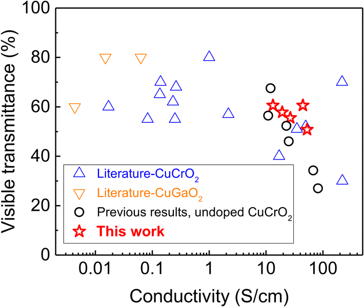 | ||
| Fig. 7 Average transmittance in the visible range vs. conductivity values for the best Mg-doped CuCrO2 samples presented in this study, and those reported in the literature for various Cu delafossites such as CuCrO2 and CuGaO2. The references used to construct this table are presented in the ESI† as Table S2. | ||
Conclusion
In conclusion, our study has successfully demonstrated the growth of compositionally controlled, Mg-doped copper chromium oxide delafossite coatings through ultrasonic spray pyrolysis. Starting from a copper deficient precursor solution, CuCrO2 samples with improved optical properties in terms of visible transmittance could be deposited. However, these samples simultaneously revealed a deficiency in electrical properties compared to films deposited from conventional 1:1 precursor solutions, which are copper rich. Notably, the introduction of magnesium divalent cations as substitutional dopants at the chromium site led to an enhancement in electrical conductivity, resulting in an order of magnitude increase (average 44.8 ± 9.6 S cm−1) compared to undoped CuCrO2 (5.5 ± 1.0 S cm−1). Importantly, this improvement in electrical conductivity was achieved while preserving optical transparency (T = 50–60%) in the visible region. Our champion sample achieved an electrical conductivity of 52.8 S cm−1 and over 60% of average visible transmittance, which translate in very high figure of merit (FoM) values for both the Haacke and Gordon's FoM, positioning compositionally adjusted, aliovalently doped copper chromium oxide as a lead contender towards high efficiency p-type transparent electrodes.
Conflicts of interest
There are no conflicts of interest to declare.Acknowledgements
The Australian Research Council is acknowledged for supporting this work through grant DP190101864. The authors acknowledge the facilities and the technical assistance of the RMIT University's Microscopy and Microanalysis Facility (RMMF).References
- R. G. Gordon, Criteria for Choosing Transparent Conductors, MRS Bull., 2000, 25(8), 52–57 CrossRef CAS.
- P. Wainer, O. Kendall, A. Lamb, S. J. Barrow, A. Tricoli, D. E. Gómez, J. van Embden and E. Della Gaspera, Continuous Growth Synthesis of Zinc Oxide Nanocrystals with Tunable Size and Doping, Chem. Mater., 2019, 31(23), 9604–9613 CrossRef CAS.
- D. S. Ginley and C. Bright, Transparent Conducting Oxides, MRS Bull., 2000, 25(8), 15–18 CrossRef CAS.
- S. C. Dixon, D. O. Scanlon, C. J. Carmalt and I. P. Parkin, n-Type doped transparent conducting binary oxides: an overview, J. Mater. Chem. C, 2016, 4(29), 6946–6961 RSC.
- G. K. Dalapati, H. Sharma, A. Guchhait, N. Chakrabarty, P. Bamola, Q. Liu, G. Saianand, A. M. Sai Krishna, S. Mukhopadhyay, A. Dey, T. K. S. Wong, S. Zhuk, S. Ghosh, S. Chakrabortty, C. Mahata, S. Biring, A. Kumar, C. S. Ribeiro, S. Ramakrishna, A. K. Chakraborty, S. Krishnamurthy, P. Sonar and M. Sharma, Tin oxide for optoelectronic, photovoltaic and energy storage devices: a review, J. Mater. Chem. A, 2021, 9(31), 16621–16684 RSC.
- J. Kim, B. J. Murdoch, J. G. Partridge, K. Xing, D. C. Qi, J. Lipton-Duffin, C. F. McConville, J. Embden and E. D. Gaspera, Ultrasonic Spray Pyrolysis of Antimony-Doped Tin Oxide Transparent Conductive Coatings, Adv. Mater. Interfaces, 2020, 7(18), 2000655 CrossRef CAS.
- J. Kim, S. Wong, G. Kim, Y.-B. Park, J. van Embden and E. Della Gaspera, Transparent electrodes based on spray coated fluorine-doped tin oxide with enhanced optical, electrical and mechanical properties, J. Mater. Chem. C, 2020, 8(41), 14531–14539 RSC.
- E. H. Kennard and E. O. Dieterich, An Effect of Light upon the Contact Potential of Selenium and Cuprous Oxide, Phys. Rev., 1917, 9(1), 58–63 CrossRef.
- B. S. Li, K. Akimoto and A. Shen, Growth of Cu2O thin films with high hole mobility by introducing a low-temperature buffer layer, J. Cryst. Growth, 2009, 311(4), 1102–1105 CrossRef CAS.
- H. Sato, T. Minami, S. Takata and T. Yamada, Transparent conducting p-type NiO thin films prepared by magnetron sputtering, Thin Solid Films, 1993, 236(1), 27–31 CrossRef CAS.
- H. Kawazoe, M. Yasukawa, H. Hyodo, M. Kurita, H. Yanagi and H. Hosono, P-type electrical conduction in transparent thin films of CuAlO2, Nature, 1997, 389(6654), 939–942 CrossRef CAS.
- R.-S. Yu and C.-M. Wu, Characteristics of p-type transparent conductive CuCrO2 thin films, Appl. Surf. Sci., 2013, 282, 92–97 CrossRef CAS.
- R. I. Sánchez-Alarcón, G. Oropeza-Rosario, A. Gutierrez-Villalobos, M. A. Muro-López, R. Martínez-Martínez, E. Zaleta-Alejandre, C. Falcony, G. Alarcón-Flores, R. Fragoso, O. Hernández-Silva, E. Perez-Cappe, Y. M. Laffita and M. Aguilar-Frutis, Ultrasonic spray-pyrolyzed CuCrO2 thin films, J. Phys. D: Appl. Phys., 2016, 49(17), 175102 CrossRef.
- L. Farrell, E. Norton, B. J. O'Dowd, D. Caffrey, I. V. Shvets and K. Fleischer, Spray pyrolysis growth of a high figure of merit, nano-crystalline, p-type transparent conducting material at low temperature, Appl. Phys. Lett., 2015, 107(3), 031901 CrossRef.
- S. Wrede and H. Tian, Towards sustainable and efficient p-type metal oxide semiconductor materials in dye-sensitised photocathodes for solar energy conversion, Phys. Chem. Chem. Phys., 2020, 22(25), 1385–13861 RSC.
- J. Wang, P. Zheng, D. Li, Z. Deng, W. Dong, R. Tao and X. Fang, Preparation of delafossite-type CuCrO2 films by sol–gel method, J. Alloys Compd., 2011, 509(18), 5715–5719 CrossRef CAS.
- J. Kim, O. Kendall, J. Ren, B. J. Murdoch, C. F. McConville, J. van Embden and E. Della Gaspera, Highly Conductive and Visibly Transparent p-Type CuCrO2 Films by Ultrasonic Spray Pyrolysis, ACS Appl. Mater. Interfaces, 2022, 14(9), 11768–11778 CrossRef CAS PubMed.
- S. Götzendörfer, C. Polenzky, S. Ulrich and P. Löbmann, Preparation of CuAlO2 and CuCrO2 thin films by sol–gel processing, Thin Solid Films, 2009, 518(4), 1153–1156 CrossRef.
- M. S. Prévot, X. A. Jeanbourquin, W. S. Bourée, F. Abdi, D. Friedrich, R. van de Krol, N. S. Guijarro, F. Le Formal and K. Sivula, Evaluating Charge Carrier Transport and Surface States in CuFeO2 Photocathodes, Chem. Mater., 2017, 29(11), 4952–4962 CrossRef.
- H. Zhang, H. Wang, W. Chen and A. K. Y. Jen, CuGaO2: A Promising Inorganic Hole-Transporting Material for Highly Efficient and Stable Perovskite Solar Cells, Adv. Mater., 2017, 29(8), 1604984 CrossRef PubMed.
- D. O. Scanlon and G. W. Watson, Understanding the p-type defect chemistry of CuCrO2, J. Mater. Chem., 2011, 21(11), 3655–3663 RSC.
- H. Kawazoe, H. Yanagi, K. Ueda and H. Hosono, Transparent p-Type Conducting Oxides: Design and Fabrication of p-n Heterojunctions, MRS Bull., 2000, 25(8), 28–36 CrossRef CAS.
- R. Nagarajan, A. D. Draeseke, A. W. Sleight and J. Tate, p-type conductivity in CuCr1−xMgxO2 films and powders, J. Appl. Phys., 2001, 89(12), 8022–8025 CrossRef CAS.
- Y. Wang, Y. Gu, T. Wang and W. Shi, Structural, optical and electrical properties of Mg-doped CuCrO2 thin films by sol–gel processing, J. Alloys Compd., 2011, 509(19), 5897–5902 CrossRef CAS.
- S. H. Lim, S. Desu and A. C. Rastogi, Chemical spray pyrolysis deposition and characterization of p-type CuCr 1− x Mg x O 2 transparent oxide semiconductor thin films, J. Phys. Chem. Solids, 2008, 69(8), 2047–2056 CrossRef CAS.
- A. Barnabé, Y. Thimont, M. Lalanne, L. Presmanes and P. Tailhades, p-Type conducting transparent characteristics of delafossite Mg-doped CuCrO2 thin films prepared by RF-sputtering, J. Mater. Chem. C, 2015, 3(23), 612–624 RSC.
- E. Chikoidze, M. Boshta, M. Gomaa, T. Tchelidze, D. Daraselia, D. Japaridze, A. Shengelaya, Y. Dumont and M. Neumann-Spallart, Control of p-type conduction in Mg doped monophase CuCrO2 thin layers, J. Phys. D: Appl. Phys., 2016, 49(20), 205107 CrossRef.
- O. Kendall, L. V. Melendez, J. Ren, S. P. Ratnayake, B. J. Murdoch, E. L. H. Mayes, J. van Embden, D. E. Gómez, A. Calzolari and E. Della Gaspera, Photoactive p-Type Spinel CuGa2O4 Nanocrystals, Nano Lett., 2023, 23(7), 2974–2980 CrossRef CAS PubMed.
- L. Bottiglieri, J. Resende, M. Weber, O. Chaix-Pluchery, C. Jiménez and J.-L. Deschanvres, Out of stoichiometry CuCrO 2 films as a promising p-type TCO for transparent electronics, Mater. Adv., 2021, 2(14), 4721–4732 RSC.
- T. S. Tripathi and M. Karppinen, Enhanced p-Type Transparent Semiconducting Characteristics for ALD-Grown Mg-Substituted CuCrO2 Thin Films, Adv. Electron. Mater., 2017, 3(6), 1600341 CrossRef.
- J. Crêpellière, P. L. Popa, N. Bahlawane, R. Leturcq, F. Werner, S. Siebentritt and D. Lenoble, Transparent conductive CuCrO2 thin films deposited by pulsed injection metal organic chemical vapor deposition: up-scalable process technology for an improved transparency/conductivity trade-off, J. Mater. Chem. C, 2016, 4(19), 4278–4287 RSC.
- D. Ling, C. Chiang, Y. Wang, Y. Lee and P. Yeh, Effect of Cr deficiency on physical properties of triangular-lattice antiferromagnets CuCr1− xO2 (0≦ x≦ 0.10), J. Appl. Phys., 2011, 109(7), 07D908 CrossRef.
- S.-Y. Kim, J.-H. Lee, J.-J. Kim and Y.-W. Heo, Effect of Ni doping on the structural, electrical, and optical properties of transparent CuCrO2 films grown using pulsed laser deposition, Ceram. Int., 2018, 44(15), 17743–17748 CrossRef CAS.
- T. S. Tripathi, J.-P. Niemelä and M. Karppinen, Atomic layer deposition of transparent semiconducting oxide CuCrO2 thin films, J. Mater. Chem. C, 2015, 3(32), 8364–8371 RSC.
- S. H. Lim, S. Desu and A. C. Rastogi, Chemical spray pyrolysis deposition and characterization of p-type CuCr1-xmgxO2 transparent oxide semiconductor thin films, J. Phys. Chem. Solids, 2008, 69(8), 2047–2056 CrossRef CAS.
- R.-S. Yu and C.-P. Tasi, Structure, composition and properties of p-type CuCrO2 thin films, Ceram. Int., 2014, 40(6), 8211–8217 CrossRef CAS.
- D.-C. Tsai, Z.-C. Chang, B.-H. Kuo, C.-M. Chen, E.-C. Chen and F.-S. Shieu, Influence of chemical composition on phase transformation and optoelectronic properties of Cu–Cr–O thin films by reactive magnetron sputtering, J. Mater. Res. Technol., 2019, 8(1), 690–696 CrossRef CAS.
- S. Nie, A. Liu, M. You, B. Shin, G. Liu and S. Fukai, Solution-processed ternary p-type CuCrO2 semiconductor thin films and their application in transistors, J. Mater. Chem. C, 2018, 6(6), 1393–1398 RSC.
- ThermoFisher Magnesium X-ray photoelectron spectra, https://www.thermofisher.com/sg/en/home/materials-science/learning-center/periodic-table/alkaline-earth-metal/magnesium.html, (assessed: October 2023).
- R. Bywalez, S. Götzendörfer and P. Löbmann, Structural and physical effects of Mg-doping on p-type CuCrO2 and CuAl0.5Cr0.5O2 thin films, J. Mater. Chem., 2010, 20(31), 6562 RSC.
- J. Resende, C. Jiménez, N. D. Nguyen and J.-L. Deschanvres, Magnesium-doped cuprous oxide (Mg:Cu2O) thin films as a transparent p-type semiconductor, Phys. Status Solidi A, 2016, 213(9), 2296–2302 CrossRef CAS.
- L. Y. Isseroff and E. A. Carter, Electronic Structure of Pure and Doped Cuprous Oxide with Copper Vacancies: Suppression of Trap States, Chem. Mater., 2013, 25(3), 253–265 CrossRef CAS.
- G. Haacke, New figure of merit for transparent conductors, J. Appl. Phys., 1976, 47(9), 4086–4089 CrossRef CAS.
- Q. Meng, S. Lu, S. Lu and Y. Xiang, Preparation of p-type CuCr1−xMgxO2 bulk with improved thermoelectric properties by sol–gel method, J. Sol-Gel Sci. Technol., 2012, 63(1), 1–7 CrossRef CAS.
Footnote |
| † Electronic supplementary information (ESI) available. See DOI: https://doi.org/10.1039/d3lf00227f |
| This journal is © The Royal Society of Chemistry 2024 |