 Open Access Article
A spin and intensity multiplexed encryption metasurface
Xuefeng
Wang
a,
Pengfei
Li
a,
Xiaoyu
Zhao
a,
Dieter
Weller
c,
Sufeng
Quan
a,
Mengxuan
Wu
a,
Ruibin
Liu
b and
Shuai
Guo
 *a
*a
aSchool of Science, Department of Optoelectronic Science, Harbin Institute of Technology at Weihai, Weihai 264209, P. R. China. E-mail: guoshuaiwh6@gmail.com
bBeijing Key Lab of Nanophotonics and Ultrafine Optoelectronic Systems, School of Physics, Beijing Institute of Technology, Beijing 100081, P. R. China
cFaculty of Physics and Center for Nanointegration (CENIDE), University of Duisburg-Essen, Duisburg 47057, Germany
First published on 7th June 2024
Abstract
Recently, metasurfaces have received widespread attention due to their superior performance in regulating the physical properties of light. In the field of optical encryption, the most common methods utilizing metasurfaces mainly include metasurface coloration, malus metasurfaces and metasurface holography. However, such methods are complex to achieve and prone to noise interference. Here, a spin and intensity multiplexed compact metasurface optical element is proposed and its feasibility for stable optical encryption is verified through simulations. Based on the photon spin Hall effect, a series of optical ciphertexts are generated with continuous changes in the spin state and intensity. As a concept demonstration, this spin and intensity multiplexed encryption metasurface will promote advanced applications of metasurfaces in many fields, such as optical communication and holography.
Introduction
A metasurface is an artificial structure array composed of a large number of sub-wavelength unit structures arranged on two-dimensional planes, which arbitrarily can modulate various parameters of incident electromagnetic waves, including phase,1–3 wavelength,4–6 polarization,7–10 orbital angular momentum,11–13etc. It is precisely because of these unique advantages that metasurfaces have become the perfect carrier for wavefront regulation.14–19 Generally speaking, in order to achieve specific functions, it is necessary to design the arrangement of meta-atoms. Due to the existence of spin–orbit interactions in anisotropic structures, the local additional geometric phase generated by meta-atoms can be induced by rotation. Because of the convenience of geometric phase modulation, this method has been widely applied in various fields, such as optical displays, optical communication, optical holography, optical micromanipulation, etc.20–28One of the most important application fields of metasurfaces is optical encryption.29–31 With the rapid development of optical and wireless communication, the security and stability of optical information transmissions are receiving increasing attention. In current research, optical encryption using metasurfaces has been achieved with many methods, including metasurface coloration, malus metasurfaces, and metasurface holography.18 For these methods, the principles are different. For example, metasurface coloration usually achieves the encryption function through resonance and malus metasurfaces use the Malus law to regulate the orthogonal polarization state and achieve encryption. As for metasurface holography, this is mainly based on using holographic algorithms to obtain encryption. These three commonly used optical encryption methods can indeed hide information with high security. However, due to processing errors and mechanism limitations, there is inevitably crosstalk in complex optical encryption systems, which leads to errors in encryption and reading.
Here, we propose a spin and intensity multiplexed metasurface with an area of 11.4 × 22.8 μm2 to achieve stable optical encryption communication of text information. The simulated change rate of the full width half maximum (FWHM) and diameter of the focal spot profiles were calculated as α1 = 3.85 nm nm−1 and α2 = 13.25 nm nm−1, respectively. By changing the intensity and spin state of the incident light, four different output states are obtained. Subsequently, through encoding the output states with binary digital signals, the optical ciphertext is achieved. Finally, by reverse decoding the optical ciphertext, optical encryption based on the design of metasurfaces is ultimately achieved. Compared with other types of optical encryption, this work proposes a simple method for encoding and transmitting information with changes of spin state and intensity. Therefore, this work proposes a scheme for the application of spin and intensity multiplexed metasurfaces in optical encryption and verifies it through simulation.
Results and discussion
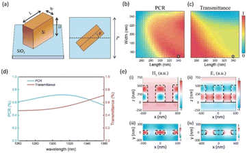
In order to manipulate the light field phase with the modulation principle of the Pancharatnam–Berry phase (P–B phase), highly anisotropic structures need to be constructed. Among them, cubic structures are an ideal solid geometry due to their ease of manufacturing. In addition, the high refractive index and high transmittance of silicon (Si) in the infrared band also indicate that it is a great material for metasurfaces. As shown in Fig. 1(a), cubic Si nanopillars are designed as the meta-atom of the array, and the substrate material is silica (SiO2). The length and width of the Si nanopillars are denoted by L and W, respectively, while the height is H, and the period of the meta-atoms is P. For incident light with the |+σ〉 spin state, the outgoing light will be a mixture of the |+σ〉 state and the |−σ〉 state, where the |±σ〉 spin states represent left and right circularly polarized light, respectively. Assuming that the rotation angle of the meta-atom is θ, the propagation phase will change correspondingly with the change of the propagation position of the light. According to the equivalent refractive index theory, the propagation phase generated at each position will not change because the size of the meta-atoms is the same. However, except for the propagation phase, the rotation angle θ of the meta-atoms will produce an additional geometric phase Φge = ei2θ due to the anisotropy of the meta-atoms. The Jones matrix of the total outgoing electric field can be calculated as follows:32 | (1) |
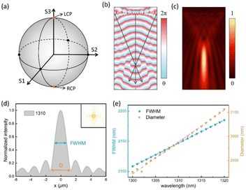
For any electromagnetic wave, the Stokes parameters can be obtained by using at least four parameters, and the calculation process of the polarization state change can be further simplified. As shown in Fig. 2(a), a Poincaré sphere is often used to describe different states of polarization. In order to achieve the convergence function, we usually use the following hyperbolic phase cross-polarization focusing formula:33
 | (2) |
Compared with the traditional focusing lens, the designed metasurface has the unique advantage of a small focusing spot size, and not being easily distorted, which mainly comes from the metasurface characteristics of small size and high integration. To evaluate the focusing spot size of the metasurface, the intensity line profile of the focus plane is further simulated, as shown in Fig. 2(d). For incident light of 1310 nm, the focusing beam diameter of the designed metasurface is about 2.975 μm. Meanwhile, the simulated focus area only accounts for about 21.4% of the metasurface area. In order to further verify the sensitivity of the metasurface to the change of incident light wavelength, the diameter and FWHM of the focus spot are simulated at different wavelengths from 1300 to 1320 nm. The relevant results are shown in Fig. 2(e). It can be seen from this figure that the FWHM of the light spot shows a great near-linear change relationship within the range of wavelength change. Therefore, through linear fitting of the data, the calculated linearity coefficients are α1 = 3.85 nm nm−1 and α2 = 13.25 nm nm−1, where α1 and α2 represent the change rate of the focus spot FWHM and diameter, respectively. This means that even tiny wavelength changes and subtle fluctuations of the incident light can be distinguished by measuring the FWHM and diameter change. With this method, the change of FWHM and diameter can be used to determine if the wavelength is 1310 nm. In optical communication systems, wavelength stability is crucial. For optical signals with the operating wavelength at 1310 nm, even subtle fluctuations in wavelength can have a serious impact on the overall transmission performance. Firstly, wavelength deviation from the optimal range of 1310 nm will lead to increased fiber optic transmission loss, thereby reducing the signal power and shortening the communication distance. At the same time, the dispersion effect will also intensify, causing signal distortion and inter-symbol interference, limiting the transmission rate and bandwidth of the system. In addition, various optoelectronic devices in communication systems, such as light sources, optical fibers, optical amplifiers, etc., are optimized and designed for the 1310 nm wavelength. If the wavelength shifts, the performance and compatibility of these devices will decrease, increasing the difficulty of system integration. Therefore, a tiny change of wavelength can lead to a series of problems and decreased performance of optical devices. This not only reduces the performance and reliability of the entire communication system, but also increases the difficulty of maintenance and repair. Therefore, maintaining high stability of the 1310 nm wavelength is one of the most important goals of optical communication systems. Through the methods mentioned in this work, we can ensure that the wavelength is 1310 nm, achieving the function of spectral purification.
In order to detect the |±σ〉 spin states simultaneously, we construct an array of 2 × 1 metasurfaces. The related phase gradients are shown as follows:
 | (3) |
 | (4) |
Due to the photonic spin Hall effect, these two sub-metasurfaces can achieve the function of converging photons with opposite spin angular momentum. If each sub-metasurface is regarded as a pixel, multiple pixels consisting of sub-metasurface arrays can realize the detection of the intensity and spin state of incident light. Based on this principle, optical encryption can be achieved with a metasurface array.
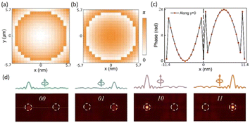
Fig. 3(a) and (b) show the phase distributions of the sub-metasurfaces of the array, which are calculated by formula (3). With the combination of two sub-metasurfaces, the metasurface array containing two pixels can be constructed. Fig. 3(c) shows the calculated phase profile of the line along the symmetric center line y = 0. When the intensity and spin state of the incident light change, the intensity and lateral position of the focus spot on the fixed object surface will also change. By changing the incident light state |Iin, ±σ〉, four different states of optical output are obtained by simulation. Simulated intensity profiles of the focal plane and intensity curves of the focal spot are shown in Fig. 3(d). In the process of optical communication, information is usually converted into binary digit (bits) for transmission. Due to the involvement of two physical parameters in optical encryption, an optical ciphertext consists of two bits of information. The optical ciphertext represents different states of incident light, where the first bit of information represents intensity and the second bit of information represents spin state. For example, the optical ciphertext “00” means that the incident light has low intensity of the |+σ〉 spin state. As a result, the conversion between the bit signal and the optical ciphertext is attainable, which serves as the fundamental principle for optical encoding and decoding.
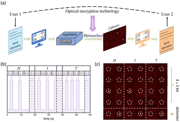
Furthermore, to achieve the encryption of a series of bits and continuous optical encryption, the designed metasurface serves as a converter between bits and optical ciphertext, as shown in Fig. 4(a). Here, user 1 wants to transmit high confidentiality secret information to user 2, taking “HIT” text content as an example. First of all, the “HIT” needs to be converted into bit signals with a combination of 0 and 1. As a process demonstration, American Standard Code for Information Interchange (ASCII) is used for the conversion of “HIT”, and the bit signal result is shown in Fig. 4(b). Between each letter, a “11” is inserted as a delimiter to identify the position of letter separation. Next, the bit signals are input into the regulator. With the continuous change of incident light, a series of optical ciphertexts can ultimately be obtained from CCD, as shown in Fig. 4(c). For every letter, the ciphertext in each column changes over time from top to bottom. In this process, each letter contains 5 optical ciphertexts due to a delimiter being included. To decode and translate the secret message, it is necessary for user 2 to compare the optical ciphertext with the standard ciphers. With the help of specially designed software, the “HIT” text encryption information can be decoded and transmitted accurately. Therefore, by using the method proposed above, optical encryption can be achieved with the designed metasurface array.
Method
The numerical simulation
The silicon metasurface is numerically simulated with the FIT and FDTD method. The Si nanopillars are placed on a SiO2 substrate with refractive indices of 3.50 and 1.45 at 1310 nm. The height of the nanopillars is fixed at 500 nm, the period at 600 nm and the lengths and widths are L and W, respectively. The polarization conversion ratio (PCR) and intensity transmittance are obtained (shown in Fig. 1) by parameter sweeping of the in-plane dimensions (L and W).Conclusions
In summary, a spin and intensity multiplexed metasurface has been proposed and the feasibility of the designed metasurface for stable optical encryption has been verified by simulation. A metasurface with an area of 11.4 × 22.8 μm2 has been designed with the hyperbolic phase distribution formula of cross-polarization focusing, which operates at the wavelength of 1310 nm. By simulating the distribution of the electromagnetic field in the image space of the metasurface, the FWHM and diameter change rate of the focal plane intensity profile are calculated as α1 = 3.85 nm nm−1 and α2 = 13.25 nm nm−1, which verifies the frequency stability in optical communication. In addition, the designed 2 × 1 metasurface array element can produce four different optical outputs by changing the intensity and spin state of the incident light. By encoding the generated four states of optical output with binary digital signals, the concept of the proposed optical encryption has been finally realized. This work proves the advantages of metasurfaces in optical encryption, and further promotes the application of metasurface optical elements in many fields, such as optical information multiplexing, optical encryption, optical data storage, etc.Conflicts of interest
There are no conflicts to declare.Acknowledgements
Funding support from the National Natural Science Foundation of China (No. 62104055), and the Natural Science Foundation of Shandong Province (No. ZR2021QF051) is acknowledged.Notes and references
- G. H. Go, C. H. Park, K. Y. Woo, M. Choi and Y. H. Cho, Nano Lett., 2023, 23, 3152–3158 CrossRef CAS
.
- S. Zhang, L. Huang, X. Li, R. Zhao, Q. Wei, H. Zhou, Q. Jiang, G. Geng, J. Li, X. Li and Y. Wang, ACS Photonics, 2021, 8, 1746–1753 CrossRef CAS
.
- A. Y. Zhu, W. T. Chen, J. Sisler, K. M. A. Yousef, E. Lee, Y. W. Huang, C. W. Qiu and F. Capasso, Adv. Opt. Mater., 2018, 7, 1801144 CrossRef
.
- J. Li, Y. Zhang, J. Li, X. Yan, L. Liang, Z. Zhang, J. Huang, J. Li, Y. Yang and J. Yao, Nanoscale, 2019, 11, 5746–5753 RSC
.
- R. Wang, M. A. Ansari, H. Ahmed, Y. Li, W. Cai, Y. Liu, S. Li, J. Liu, L. Li and X. Chen, Light: Sci. Appl., 2023, 12, 103 CrossRef CAS
.
- Y. Ni, C. Chen, S. Wen, X. Xue, L. Sun and Y. Yang, eLight, 2022, 2, 23 CrossRef
.
- Y. Intaravanne, R. Wang, H. Ahmed, Y. Ming, Y. Zheng, Z. K. Zhou, Z. Li, S. Chen, S. Zhang and X. Chen, Light: Sci. Appl., 2022, 11, 302 CrossRef CAS
.
- J. Yang, R. Zhao, Y. Li, H. Xiong, Y. Li, X. Li, J. Li, Y. Wang and L. Huang, Adv. Opt. Mater., 2023, 11, 202202896 Search PubMed
.
- Z. Zhang, J. Luo, M. Song and H. Yu, Appl. Phys. Lett., 2015, 107, 24 Search PubMed
.
- R. Zhao, G. Geng, Q. Wei, Y. Liu, H. Zhou, X. Zhang, C. He, X. Li, X. Li, Y. Wang, J. Li and L. Huang, Adv. Opt. Mater., 2022, 10, 2102596 CrossRef CAS
.
- M. Liu, P. Huo, W. Zhu, C. Zhang, S. Zhang, M. Song, S. Zhang, Q. Zhou, L. Chen, H. J. Lezec, A. Agrawal, Y. Lu and T. Xu, Nat. Commun., 2021, 12, 2230 CrossRef CAS
.
- H. Wang, H. Wang, Q. Ruan, J. Y. E. Chan, W. Zhang, H. Liu, S. D. Rezaei, J. Trisno, C. W. Qiu, M. Gu and J. K. W. Yang, Nat. Nanotechnol., 2023, 18, 264 CrossRef CAS
.
- M. I. Shalaev, J. Sun, A. Tsukernik, A. Pandey, K. Nikolskiy and N. M. Litchinitser, Nano Lett., 2015, 15, 6261–6266 CrossRef CAS
.
- J. B. Pendry, D. Schurig and D. R. Smith, Science, 2006, 312, 1780–1782 CrossRef CAS
.
- R. Zhao, L. Huang and Y. Wang, PhotoniX, 2020, 1, 20 CrossRef
.
- V. S. Asadchy, A. Díaz-Rubio and S. A. Tretyakov, Nanophotonics, 2018, 7, 1069–1094 CAS
.
- J. Hu, S. Bandyopadhyay, Y.-H. Liu and L.-Y. Shao, Front. Phys., 2021, 8, 586087 CrossRef
.
- C. Jung, G. Kim, M. Jeong, J. Jang, Z. Dong, T. Badloe, J. K. W. Yang and J. Rho, Chem. Rev., 2021, 121, 13013–13050 CrossRef CAS
.
- J. Yang, S. Gurung, S. Bej, P. Ni and H. W. Howard Lee, Rep. Prog. Phys., 2022, 85, 3 CrossRef
.
- W. Ye, F. Zeuner, X. Li, B. Reineke, S. He, C. W. Qiu, J. Liu, Y. Wang, S. Zhang and T. Zentgraf, Nat. Commun., 2016, 7, 11930 CrossRef CAS
.
- G. Qu, W. Yang, Q. Song, Y. Liu, C.-W. Qiu, J. Han, D.-P. Tsai and S. Xiao, Nat. Commun., 2020, 11, 5484 CrossRef CAS
.
- Q. Song, X. Liu, C.-W. Qiu and P. Genevet, Appl. Phys. Rev., 2022, 9, 011311 CAS
.
- C. Qian, X. Lin, X. Lin, J. Xu, Y. Sun, E. Li, B. Zhang and H. Chen, Light: Sci. Appl., 2020, 9, 59 CrossRef CAS
.
- J. Li, Z. Guan, H. C. Liu, Z. He, Z. Li, S. Yu and G. Zheng, Laser Photonics Rev., 2022, 17, 2200342 CrossRef
.
- S. Yu, L. Li, G. Shi, C. Zhu and Y. Shi, Appl. Phys. Lett., 2016, 108, 241901 CrossRef
.
- X. Ou, T. Zeng, Y. Zhang, Y. Jiang, Z. Gong, F. Fan, H. Jia, H. Duan and Y. Hu, Nano Lett., 2022, 22, 10049–10056 CrossRef CAS
.
- G.-Y. Lee, J.-Y. Hong, S. Hwang, S. Moon, H. Kang, S. Jeon, H. Kim, J.-H. Jeong and B. Lee, Nat. Commun., 2018, 9, 4562 CrossRef
.
- J. Kim, J. Seong, W. Kim, G. Y. Lee, S. Kim, H. Kim, S. W. Moon, D. K. Oh, Y. Yang, J. Park, J. Jang, Y. Kim, M. Jeong, C. Park, H. Choi, G. Jeon, K. I. Lee, D. H. Yoon, N. Park, B. Lee, H. Lee and J. Rho, Nat. Mater., 2023, 22, 474–481 CrossRef CAS
.
- J. Kim, D. Jeon, J. Seong, T. Badloe, N. Jeon, G. Kim, J. Kim, S. Baek, J.-L. Lee and J. Rho, ACS Nano, 2022, 16, 3546–3553 CrossRef CAS
.
- Y. Hu, X. Luo, Y. Chen, Q. Liu, X. Li, Y. Wang, N. Liu and H. Duan, Light: Sci. Appl., 2019, 8, 86 CrossRef
.
- L. Deng, J. Deng, Z. Guan, J. Tao, Y. Chen, Y. Yang, D. Zhang, J. Tang, Z. Li, Z. Li, S. Yu, G. Zheng, H. Xu, C.-W. Qiu and S. Zhang, Light: Sci. Appl., 2020, 9, 101 CrossRef CAS
.
- I. Kim, J. Jang, G. Kim, J. Lee, T. Badloe, J. Mun and J. Rho, Nat. Commun., 2021, 12, 3614 CrossRef CAS
.
- L. Zhang, S. Chang, X. Chen, Y. Ding, M. T. Rahman, Y. Duan, M. Stephen and X. Ni, Nano Lett., 2023, 23, 51–57 CrossRef CAS
.
| This journal is © The Royal Society of Chemistry 2024 |


