 Open Access Article
Creative Commons Attribution 3.0 Unported Licence
Electronic structure of thin MoS2 films†
Benjamin A.
Chambers
ab,
Christopher T.
Gibson
ab and
Gunther G.
Andersson
 *ab
*ab
aFlinders Institute for NanoScale Science and Technology, Flinders University, Adelaide, SA 5001, Australia. E-mail: gunther.andersson@flinders.edu.au; Tel: +61 8 82012309
bFlinders Microscopy and Microanalysis, College of Science and Engineering, Flinders University, Bedford Park, SA 5042, Australia
First published on 29th July 2024
Abstract
The valence electron structure of exfoliated monolayer MoS2 deposited onto SiO2 was determined by UV photoelectron spectroscopy through component analysis in combination with Auger electron microscopy. The valence electron cut-off for bulk MoS2 was found at 0.64 eV binding energy whilst monolayer MoS2 and few layer MoS2 have higher binding energies of 0.89 eV and 1.26 eV respectively. SiO2 is known to interact only weakly with MoS2. Thus, the valence electron structure of higher binding energy determined here is thus considered to represent that of a material not affected by strain. The implications of the change in the valence electron cut-off are discussed.
Introduction
MoS2 is an example of a transition metal dichalcogenide that possesses an indirect bandgap with a transition from indirect to direct band gap when transitioning from bulk to few or monolayer thickness experimentally and through computer simulations.1–4 The structure of MoS2 allows fabricating monolayers through exfoliation1 or growth on substrates.5–7 The charges on the surface and in the bulk of MoS2 are almost identical which is related to the van der Waals type bonding between layers.8 The electronic and optical properties of MoS2 are changing with the number of monolayers9–12 and at the edges of the crystallites.13 Changing the numbers of monolayers forming a sample allows for tuning its properties – also through combining with other metal dichalcogenides9 – for a range of applications such as energy conversion and storage14 and biomedical applications.15 A challenge in using monolayer MoS2 is fabricating the material as large scale crystallites.16 Several calculations of the band structure of monolayer MoS2 have been conducted.17–21 Reducing the thickness of the material from bulk to a monolayer also increases the bandgap overall.22 An increase of the band gap of MoS2 from 1.29 eV to 1.9 eV was found by Mak et al.1 It has been reported that with a fine control over the number of layers forming a MoS2, the work function of a surface may be tuned allowing for surfaces to be tuned for specific interfacing and the surface potential can be changed.23 The electronic properties such as the band structure and exciton binding energies and the geometric properties of a MoS2 sample change when strain is introduced into a sample.17,24,25 The properties of MoS2 can also be changed through doping.19Direct measurements of the band structure of MoS2 are rare and difficult to perform. The reason is that photoelectron spectroscopy, as the method typically used for investigating the electronic structure of surfaces, probes several monolayers at a sample surface and in case of monolayer MoS2 therefore the monolayer plus the top few layers of the substrate. The resulting spectra thus show the density of states (DOS) of the monolayer MoS2 plus that of the substrate.25–28 One of the few examples of measuring the DOS of monolayer MoS2 are from Eknapakul et al. who determined the band structure of monolayer MoS2 with intercalated potassium layers with angle resolved photoelectron spectroscopy (ARPES).5 However, due to the presence of the K interlayers the results found through this work have to be considered to differ from monolayer MoS2. This situation leaves the literature of investigating MoS2 monolayers deposited onto substrates with a situation that the electron spectrum of MoS2 is known with a high degree of plausibility but not with spectra of MoS2 only.
It is an intrinsic problem of all methods of photoelectron spectroscopy that in the of investigating monolayer materials deposited onto a substrate, that the contribution of the monolayer and the substrate cannot be separated unless the spectrum of the substrate covers an entirely different electron binding energy range compared to the monolayer material. The latter is usually not the case. This problem could only be overcome by applying an electron spectroscopy method which is sensitive to the outermost layer only such as metastable induced electron spectroscopy (MIES) or by applying a procedure in the data evaluation which allows to separate the contributions of the monolayer and the substrate. The disadvantage of MIES is that it would be sensitive only to the outer electronic structure of the monolayer and not to the overall monolayer. We thus have chosen in the present work a different route and applied a component analysis method for the data evaluation. The variation of the surface coverage with MoS2 can be used as advantage in a component analysis because it introduces a variation in the contribution of the substrate and the monolayer to the spectra taken from various spots of the sample and allows for a mathematical separation of the spectral contributions of monolayer and substrate. The method developed in this work can in general be used for investigating any monolayer material deposited onto a substrate.
The aim of the present work is to determine experimentally the valence electron structure of monolayer MoS2. UV photoelectron spectroscopy (UPS) is applied, and the data are processed through component analysis separating the spectral contributions of the monolayer MoS2 and that of the substrate. The data processing also allows to separate the spectra of monolayer and few layer MoS2 showing the transition of the valence electron structure from the monolayer over the few layer to bulk MoS2. We have chosen a Si wafer with naturally oxidised SiO2 as substrate. SiO2 is known to interact only weakly with the MoS2 monolayer29 which we assume is holding also in the present case. In this way the valence electron structure of monolayer MoS2 can be determined where the valence electron structure is only weakly modified through the interaction with the substrate. The combination of careful preparation of a sample containing mainly monolayer MoS2 and some few layer MoS2 with the component analysis of the electron spectra allows to show experimentally the change of the valence band edge with the thickness of MoS2.
Experimental
Materials and sample preparation
X-ray photoelectron spectroscopy and ultraviolet photo electron spectroscopy
The MoS2 samples were investigated using XPS and UPS in an ultra-high vacuum (UHV) system built by SPECS (Berlin, Germany) which has a base pressure of a few 10−10 mbar. The He* and UV light (He I line) were generated in a two stage cold cathode gas discharge from MFM Analytical Systems (Claustal-Zellerfeld, Germany). A non-monochromatic X-ray source is used to generate Mg Kα radiation. For detecting the emitted electrons a hemispherical Phoibos 100 energy analyser from SPECS (Berlin, Germany) was used. UPS and XPS were recorded at a pass energy of 10 eV and a bias of −10 V was applied to the samples for the UPS and metastable induced electron spectroscopy (MIES) measurements. The angle of UV and X-ray source radiation and the analyser are both 54° with respect to the surface normal of the sample. High resolution XP spectra were fitted with combined Gaussian–Lorentzian components and a correction for the Shirley background.30 For quantification of relative intensities the cross sections calculated by Yeh have been used.31For UPS the samples were irradiated with UV photons from the HeI line (hν = 21.2 eV). The photons excite the valence electrons through the photoelectric effect. For HeI UPS the surface sensitivity is limited by the electron mean free path to the upper 2–3 nm of the sample.32 The binding energy of the electrons in the sample is determined by eqn (1).
| Ebinding = 21.2 eV − Ekinetic − Φspec | (1) |
MIES was applied at the same time as UPS. The MIE spectra have no significant features in the region up to 6 eV. The reason in the present case is that MoS2 has states at low binding energy which favours the resonance ionisation (RI) followed by Auger neutralisation (AN) mechanism for the deexcitation of the metastable He atoms.33
While running UPS and MIES, the measurements were monitored for evidence of charging. As a routine, the measurements are conducted in a sequence of acquiring three spectra consecutively with the first two spectra consisting of single scans only. The samples are started to be exposed to UV photons and He* just before the data acquisition is started. This is facilitated by keeping the valve between the UV and He* source and the analysis chamber of the equipment closed until the data acquisition starts. In case the secondary onset of the measurements stays stable without showing a shift between the three measurements, charging of the sample during the measurements can reasonably be excluded. We also did not find charging of the MoS2 during the XPS measurement.
Scanning electron microscopy and auger electron spectroscopy
The MoS2 on SiO2 samples were analysed with a PHI710 Scanning Auger Nanoprobe (Flinders Microscopy and Microanalysis, Flinders University) with an electron energy of 1 keV. Auger electron spectroscopy (AES) is a similar spectroscopic technique to XPS. The sample is irradiated with an electron beam with a kinetic energy of the electrons from 1 to 25 keV which results in the excitation of electrons in the sample leading to their emission. In the present work 10 keV electrons were used. The atom from which an electron is emitted is in an excited state which subsequently transits to the ground state leading to the emission of an Auger electron with an energy characteristic for the specific element. The emission of the electrons is detected with a detector with spatial resolution similar to that of the scanning electron microscope (SEM) allowing spatially resolved elemental mapping of the surface. AES and AEM can be combined in one instrument which is called Auger electron microscopy (AEM). AEM has an advantage over SEM in conjunction with energy-dispersive X-ray spectroscopy (EDX) due to the surface sensitivity of AEM.Heating procedure
Before applying electron spectroscopy, the samples were heated to 723 K.Measurement procedure
XPS and UPS were measured on nine different locations using a medium magnification lens mode with a diameter of the spot size for the analysis of 1.4 mm. This allows for applying a component analysis to separate the components in UPS the spectra related to the various thickness of MoS2 and the substrate. The central spot is located approximately in the middle of the MoS2 shown in Fig. S1.† The other nine spots are located +2 mm or −2 mm to the left and right and top and bottom of the central spot. As an example, the spot (x, z) +2/−2 is located 2 mm above and 2 mm to the left of the central spot.SVD analysis
A mathematical algorithm known as singular value decomposition (SVD) is used to analyse a series of UP spectra. The details of the procedure can be found in literature.34–36 A summary is provided in the ESI.† The SVD procedure results in reference spectra which are used to reproduce the measured UP spectra as linear combination. The reference spectra represent spectra of a surface with a specific composition and electronic structure.Raman spectroscopy
Raman spectra were acquired using a WITec alpha 300 R Raman microscope at an excitation laser wavelength of 532 nm (≤5 mW) with a ×40 objective (numerical aperture 0.60). A minimum of 15 Raman spectra were recorded per sample at approximately 5 separate locations within each sample. Typical integrations times were 10–30 s for 2–3 accumulations per spectrum.Results and discussion
SEM imaging
In Fig. 1 a SEM image of the central part of the sample is shown. Triangular shaped features with medium grey scale brightness can be identified as thin MoS2 crystallites with the help of Auger microscopy and Raman spectroscopy (see Fig. S2 and S3 in the ESI†). Between the grey triangle areas lighter grey areas can be seen which is the uncovered Si wafer used as substrate. Additionally, some darker areas with overlap between the triangular crystallites can be identified and some dark areas with arbitrary shape. The latter will be identified below as contamination. The area analysis from Fig. 1 is shown in Table 1 with single MoS2 sheets covering 61.4% of the surface, thicker MoS2 covering 0.7%, contaminations covering 0.8% and the substrate representing 30.7% of the surface. The analysis of the coverage was done by a grey scale histogram analysis of the SEM image.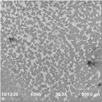 | ||
| Fig. 1 SEM image of the central area of the sample shown in Fig. S1.† The dark grey triangular shaped areas are the monolayer MoS2 crystallites. The crystallites show a small degree of overlap. The relative fraction of the sample surface formed by the substrate, monolayer and few layer MoS2 is provided in Table 1. | ||
| Species | Fraction area [%] |
|---|---|
| Substrate (light grey), silicon wafer | 30.7 |
| MoS2, thin (medium light grey) | 61.4 |
| MoS2, thick (medium dark grey) | 0.7 |
| Contamination (dark grey) | 0.8 |
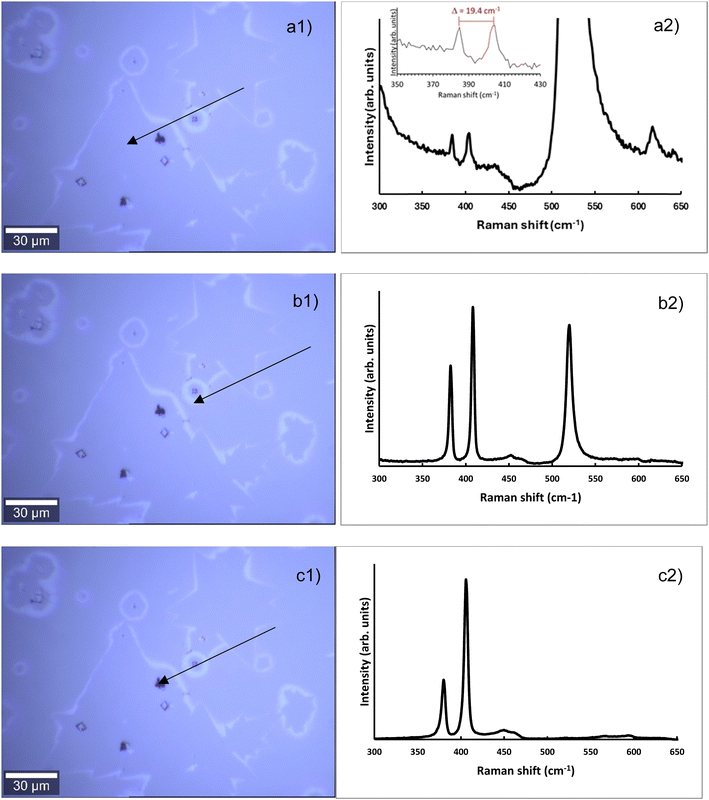
Fig. S1† shows an optical image of the MoS2. In Fig. 2 examples of key positions chosen to conduct Raman spectroscopy for evaluating the structural properties of the MoS2 are shown. The respective Raman spectra are displayed adjacent to the indicated positions. The optical image itself appears to have triangular crystalline structures which corresponds to the expected shape of MoS2 crystallites.10
The first region within the triangular crystalline shape appeared to be MoS2 with peaks at 384.8 and 404.5 cm−1 representing the E12g and A1g modes, respectively. The separation of these peaks (19.4 ± 0.5 cm−1) combined with the high intensity of the silicon peak at 520 cm−1 indicates monolayer MoS2 in this region.29 The peak separation of 19.7 cm−1 is between those found for monolayer MoS2 on Al2O3 (18 cm−1) and Au (21 cm−1) were for the first substrate tensile strain and for the second compressive strain has been reported.37 This finding is supporting the assumption that SiO2 as substrate used here results only in a weak interaction between the substrate and the MoS2 monolayer. The second location, a white cloudlike region, still has MoS2, however the reduced silicon peak intensity, relative to the MoS2 peaks, indicates a higher MoS2 concentration. The MoS2 peaks are situated at 382.5 cm−1 and 408.5 cm−1 and are separated by 26 cm−1. This separation combined with the higher MoS2 concentration than the monolayer indicates multilayer MoS2.29,38 The last region which is a dark black spot on the optical image possesses high intensity MoS2 peaks at 380.0 cm−1 and 406.0 cm−1 with no visible silicon peaks. The MoS2 is thus thick enough to obstruct the detection of the silicon substrate and is classified as bulk MoS2.
For better identifying the chemical nature of the crystallites AEM was applied. In the ESI† Fig. S2a shows SEM images indicating the position of the spots from which Auger spectra were taken with the latter shown in Fig. S2b.† The triangular shaped features with medium grey scale brightness can be identified as thin MoS2 crystallites. Fig. S2a† shows an SEM image of a similar sample with a single triangle in position 5 identified by AES as having very low Mo and S content being linked to monolayer MoS2.The Auger spectra clearly identify that the deposited triangular shaped material in MoS2.
In the ESI† in Fig. S3 Raman spectra of one of the triangular crystallites are shown. From the Raman spectra the vast majority of the area of the triangular crystals can be identified as monolayer MoS2 based on the separation of the E12g and A1g modes.29 A small fraction of the crystallite area formed is few layer MoS2.
XPS analysis
In Fig. 3 the high resolution XP spectra of the sample are shown with the binding energies of all components found listed in Table 2. In Fig. 3a the C1s spectrum is shown. The components are C1 at 285 (sp3 C–C), C2 at 286.5 ± 0.2 eV assigned to C–O (ref. 39) or C–OH (ref. 40) or similar bonds, C3 at 288.0 ± 0.2 eV assigned to C![[double bond, length as m-dash]](https://www.rsc.org/images/entities/char_e001.gif) O (ref. 40) and C4 at 289.8 ± 0.2 eV assigned to C(O)OH.40 All these carbon species are adventitious carbon. Their specific nature is not relevant for the present work. In Fig. 3b the Mo 3p doublet is shown with the 3p3/2 peak at 395.9 ± 0.2 eV which can be identified as Mo in MoS2.41 A small peak for MoO3 was found at 399.5 ± 0.2 eV (ref. 41) with 16% of the overall Mo intensity. This Mo peak is not the main peak for Mo in XPS. However, the main Mo 3d5/2 peak at around 228 eV is overlapping with the S 2s peak and for this reason could not be used for the data analysis. In Fig. 3c the S 2p doublet is shown with the 2p3/2 peak at 162.8 ± 0.2 eV which can be identified as Mo in MoS2.42 In Fig. 3c the O 1s spectrum with one component O1 at 533.9 ± 0.2 eV and a second small component at 531.7 ± 0.2 eV. The first is O of SiO2 (ref. 43) while the latter is probably adventitious OH. In Fig. 3d the Si 2p region with two doublets are shown. The 2p3/2 peak of one doublet is found at 99.9 ± 0.2 eV and can be identified as Si while the second doublet is at 104.5 ± 0.2 eV which can be identified as SiO2.43 The ratio of Mo to S based on the relative intensities shown in Table 2 is 0.49 ± 0.02 thus corresponds to the stoichiometric ratio of the two elements.
O (ref. 40) and C4 at 289.8 ± 0.2 eV assigned to C(O)OH.40 All these carbon species are adventitious carbon. Their specific nature is not relevant for the present work. In Fig. 3b the Mo 3p doublet is shown with the 3p3/2 peak at 395.9 ± 0.2 eV which can be identified as Mo in MoS2.41 A small peak for MoO3 was found at 399.5 ± 0.2 eV (ref. 41) with 16% of the overall Mo intensity. This Mo peak is not the main peak for Mo in XPS. However, the main Mo 3d5/2 peak at around 228 eV is overlapping with the S 2s peak and for this reason could not be used for the data analysis. In Fig. 3c the S 2p doublet is shown with the 2p3/2 peak at 162.8 ± 0.2 eV which can be identified as Mo in MoS2.42 In Fig. 3c the O 1s spectrum with one component O1 at 533.9 ± 0.2 eV and a second small component at 531.7 ± 0.2 eV. The first is O of SiO2 (ref. 43) while the latter is probably adventitious OH. In Fig. 3d the Si 2p region with two doublets are shown. The 2p3/2 peak of one doublet is found at 99.9 ± 0.2 eV and can be identified as Si while the second doublet is at 104.5 ± 0.2 eV which can be identified as SiO2.43 The ratio of Mo to S based on the relative intensities shown in Table 2 is 0.49 ± 0.02 thus corresponds to the stoichiometric ratio of the two elements.
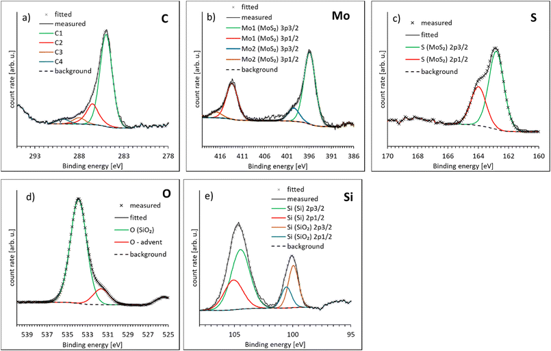 | ||
| Fig. 3 XP spectra of a) C1s, b) Mo 3p, c) S 2p, d) O 1s. and e) Si 2p. The measured spectra are shown together with the fit of Shirley background and the spectral components. | ||
| Component | Chemical species | Binding energy ± 0.2 [eV] | Rel. intensities [%] |
|---|---|---|---|
| C1–C1s | C–C sp3, adventitious | 285 | 13.2 ± 0.3 |
| C2–C1s | C–O or C–OH,39 adventitious | 286.5 | 3.3 ± 0.3 |
| C3–C1s | C![[double bond, length as m-dash]](https://www.rsc.org/images/entities/char_e001.gif) O,40 adventitious O,40 adventitious |
288.0 | 0.9 ± 0.3 |
| C4–C1s | C(O)OH,40 adventitious | 289.8 | 0.7 ± 0.3 |
| Mo | MoS2 (ref. 41) | 395.9 | 3.4 ± 0.1 |
| Mo | MoO3 (ref. 41) | 399.5 | 0.6 ± 0.1 |
| S | MoS2 (ref. 42) | 162.8 | 7.0 ± 0.1 |
| O1 | SiO2 (ref. 43) | 533.9 | 36.4 ± 0.4 |
| O2 | OH, adventitious | 531.7 | 5.6 ± 0.4 |
| Si1 | Si (ref. 43) | 99.9 | 8.0 ± 0.2 |
| Si2 | SiO2 (ref. 43) | 104.5 | 20.9 ± 0.2 |
The combined relative intensities of MoS2 of 12.1% are compatible with a MoS2 layer thickness of approximately 4 Å at a coverage of 60%.
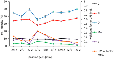
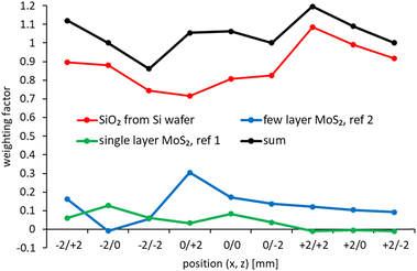
In Fig. 4 the relative intensities of the elements detected with XPS for all nine spots are shown. It can be seen that the coverage with MoS2 is highest in the centre of the sample along the x-axis, i.e. at x = 0.
UPS analysis
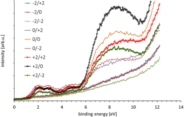
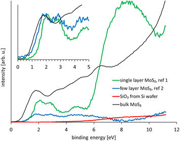
In Fig. 5 the UP spectra of all nine spots analysed are shown. The components of the series of the nine spectra were analysed with SVD. SVD has been proven to be a powerful data analysis tool when the various components of a sample cannot physically be separated for the process of the analysis. SVD has been successfully applied to separate in electron spectroscopy the various components at liquid surfaces and solid surfaces,44 clusters on surfaces45 and interfaces in organic electronics.46The reference spectra resulting from the SVD analysis are shown in Fig. 6 and the weighting factors for the reference spectra are shown in Fig. 7. These reference spectra represent the components forming the sample and the weighting factor the fraction of their contribution to the measured spectra. The spectrum of bulk MoS2 is also shown. Two reference spectra were found representing MoS2. The first reference spectrum is assigned to single monolayer of MoS2. The reason for this assignment is that the spectrum shows the characteristic structure of MoS2 similar to the bulk MoS2 in the region 6 eV binding energy. Additionally, this reference spectrum shows a broad distribution between 6 and 10 eV which is characteristic for SiO2. Thus the first reference spectrum is a combination of the spectrum from single layer MoS2 and SiO2 with the later contributing only intensity at binding energies >6 eV. The part of the spectrum at <6 eV thus can be assigned exclusively to monolayer MoS2. The second reference spectrum is also assigned to MoS2. In contrast to the first reference spectrum it does not show the broad SiO2 feature between 6 and 10 eV. The second reference spectrum is assigned to stacking of monolayer MoS2 forming bilayers as it could be identified from Fig. 1. The valence electron cut-off is at a binding energy between monolayer and bulk MoS2. This MoS2 species is referred here to “few” layer. Although it is likely that this species is a double layer, we refer here to “few” because we cannot provide unambiguous evidence for a double layer species. The third reference spectrum is assigned to SiO2 showing only the broad distribution between 6 and 10 eV characteristic for SiO2.
In Fig. 4 the sum of the weighting factors for the first and second MoS2 spectra are shown. It can be seen that the sum of the MoS2 weighting factors follows closely the relative intensities of Mo and S in XPS confirming the assignment of reference spectra 1 and 2 to MoS2.
The valence band (VB) cut-off for bulk MoS2 is found at 0.64 ± 0.05 eV as can be seen in Fig. S3 which is similar to what was found by Timpel et al. for annealed MoS2.2 Comparing the VB cut-off of both reference spectra with that of bulk MoS2 it can be seen in the inset of Fig. 6 that the single layer MoS2 is shifted by about 0.6 eV to higher binding energies of 1.26 eV and the few layer MoS2 by about 0.25 eV to 0.89 eV; the respective VB cut-offs are also shown in Fig. S3.†
The shift in the VB cut-off is consistent with the increase in band gap found by Mak et al. who found an increase in band gap from 6 to 1 monolayer MoS2 of 0.5 eV.1 In case the conduction band (CB) cut-off does not move at the same time to lower energies, the band gap of the single and double layer MoS2 has increased. Mak et al. found a shift in band gap of almost the same amount as found here for the change of the valence band edge for the transition from bulk to monolayer MoS2, and it could be hypothesised that the CB position does not change at the same time. However, computer calculations show a decrease in the CB position with increasing number of MoS2 layers which also would contribute to a decrease of the band gap of MoS2 with increasing number of layers. It should be noted that it would be needed to measure the position of the conduction band for MoS2 with a variation of the number of layers, which should be possible with a technique like inverse photoemission spectroscopy.28
The VB cut-off found by Eknapul et al. of MoS2 with an interlayer of K is found at 1.89 eV which is larger than what is found in the present work. The reason might be the interaction of MoS2 with the K interlayer. Interaction with substrates had been found by Park et al. who reported a VB cut-off for MoS2 on SiO2 of 1.81 eV and on Au of 1.30 eV.27 Park et al. have used the same preparation as in the present work. It is unclear why the VB cut-off reported by these authors is different to our work.
Conclusion
We have determined the valence electron structure of monolayer MoS2 deposited onto SiO2 with UPS. Component analysis of UP spectra acquired in a spatially resolved mode separating various areas of the sample with mm resolution in combination with SEM and spatially resolved XPS have been used to separate the components in the UP spectra. The valence electron of MoS2 only weakly interacting with the SiO2 substrate shows a VB cut-off which is at 0.6 eV higher binding energy than bulk MoS2. The double layer shows an increase in the binding energy of the cut-off of 0.25 eV.Data availability
All data supporting this article have been included either in the main manuscript or in the ESI.†Conflicts of interest
There is no conflict of interest to be reported.Acknowledgements
This work was supported by the College of Science and Engineering at Flinders University and by a grant of the Australian Research Council (LE0989068). The authors would like to thank Anthony George and Andrey Turchanin of the Institute of Physical Chemistry at the Friedrich Schiller University in Jena (Germany) for providing the monolayer MoS2 samples. The authors acknowledge the facilities, and the scientific and technical assistance, of Microscopy Australia (formerly known as AMMRF) and the Australian National Fabrication Facility (ANFF) at Flinders University. The authors would also like to acknowledge the expertise and support provided by Flinders Microscopy and Microanalysis (FMMA).References
- K. F. Mak, C. Lee, J. Hone, J. Shan and T. F. Heinz, Atomically Thin MoS2: A New Direct-Gap Semiconductor, Phys. Rev. Lett., 2010, 105, 136805 CrossRef PubMed
.
- M. Timpel, G. Ligorio, A. Ghiami, L. Gavioli, E. Cavaliere, A. Chiappini, F. Rossi, L. Pasquali, F. Gärisch, E. J. W. List-Kratochvil, P. Nozar, A. Quaranta, R. Verucchi and M. V. Nardi, 2D-MoS2 goes 3D: transferring optoelectronic properties of 2D MoS2 to a large-area thin film, npj 2D Mater. Appl., 2021, 5, 64 CrossRef CAS
.
- J. Kang, L. Zhang and S.-H. Wei, A Unified Understanding of the Thickness-Dependent Bandgap Transition in Hexagonal Two-Dimensional Semiconductors, J. Phys. Chem. Lett., 2016, 7, 597–602 CrossRef CAS PubMed
.
- L. Zhang and A. Zunger, Evolution of Electronic Structure as a Function of Layer Thickness in Group-VIB Transition Metal Dichalcogenides: Emergence of Localization Prototypes, Nano Lett., 2015, 15, 949–957 CrossRef CAS PubMed
.
- T. Eknapakul, P. D. C. King, M. Asakawa, P. Buaphet, R. H. He, S. K. Mo, H. Takagi, K. M. Shen, F. Baumberger, T. Sasagawa, S. Jungthawan and W. Meevasana, Electronic Structure of a Quasi-Freestanding MoS2 Monolayer, Nano Lett., 2014, 14, 1312–1316 CrossRef CAS PubMed
.
- A. Winter, A. George, C. Neumann, Z. Tang, M. J. Mohn, J. Biskupek, N. Masurkar, A. L. M. Reddy, T. Weimann, U. Hübner, U. Kaiser and A. Turchanin, Lateral heterostructures of two-dimensional materials by electron-beam induced stitching, Carbon, 2018, 128, 106–116 CrossRef CAS
.
- A. George, C. Neumann, D. Kaiser, R. Mupparapu, T. Lehnert, U. Hübner, Z. Tang, A. Winter, U. Kaiser, I. Staude and A. Turchanin, Controlled growth of transition metal dichalcogenide monolayers using Knudsen-type effusion cells for the precursors, JPhys Mater., 2019, 2, 016001 CrossRef CAS
.
- G. U. Von Oertzen, S. L. Harmer and W. M. Skinner, XPS and ab initio calculation of surface states of sulfide minerals: pyrite, chalcopyrite and molybdenite, Mol. Simul., 2006, 32, 1207–1212 CrossRef CAS
.
- W. Choi, N. Choudhary, G. H. Han, J. Park, D. Akinwande and Y. H. Lee, Recent development of two-dimensional transition metal dichalcogenides and their applications, Mater. Today, 2017, 20, 116–130 CrossRef CAS
.
- X. Yang and B. Li, Monolayer MoS2 for nanoscale photonics, Nanophotonics, 2020, 9, 1557–1577 CrossRef CAS
.
- F. G. Aras, A. Yilmaz, H. G. Tasdelen, A. Ozden, F. Ay, N. K. Perkgoz and A. Yeltik, A review on recent advances of chemical vapor deposition technique for monolayer transition metal dichalcogenides (MX2: Mo, W; S, Se, Te), Mater. Sci. Semicond. Process., 2022, 148, 106829 CrossRef CAS
.
- I. Paradisanos, S. Shree, A. George, N. Leisgang, C. Robert, K. Watanabe, T. Taniguchi, R. J. Warburton, A. Turchanin, X. Marie, I. C. Gerber and B. Urbaszek, Controlling interlayer excitons in MoS2 layers grown by chemical vapor deposition, Nat. Commun., 2020, 11, 2391 CrossRef CAS PubMed
.
- T.-X. Huang, X. Cong, S.-S. Wu, K.-Q. Lin, X. Yao, Y.-H. He, J.-B. Wu, Y.-F. Bao, S.-C. Huang, X. Wang, P.-H. Tan and B. Ren, Probing the edge-related properties of atomically thin MoS2 at nanoscale, Nat. Commun., 2019, 10, 5544 CrossRef CAS PubMed
.
- J. Theerthagiri, R. A. Senthil, B. Senthilkumar, A. Reddy Polu, J. Madhavan and M. Ashokkumar, Recent advances in MoS2 nanostructured materials for energy and environmental applications – A review, J. Solid State Chem., 2017, 252, 43–71 CrossRef CAS
.
- U. Yadav, H. Mishra, V. Singh, S. Kashyap, A. Srivastava, S. Yadav and P. S. Saxena, Enhanced Osteogenesis by Molybdenum Disulfide Nanosheet Reinforced Hydroxyapatite Nanocomposite Scaffolds, ACS Biomater. Sci. Eng., 2019, 5, 4511–4521 CrossRef CAS PubMed
.
- Y. Liu and F. Gu, A wafer-scale synthesis of monolayer MoS2 and their field-effect transistors toward practical applications, Nanoscale Adv., 2021, 3, 2117–2138 RSC
.
- H. L. Zhu, C. J. Zhou, X. J. Huang, X. L. Wang, H. Z. Xu, Y. Lin, W. H. Yang, Y. P. Wu, W. Lin and F. Guo, Evolution of band structures in MoS2-based homo- and heterobilayers, J. Phys. D: Appl. Phys., 2016, 49, 065304 CrossRef
.
- M.-T. Wu, J.-W. Fan, K.-T. Chen, S.-T. Chang and C.-Y. Lin, Band Structure and Effective Mass in Monolayer MoS2, J. Nanosci. Nanotechnol., 2015, 15, 9151–9157 CrossRef CAS PubMed
.
- C. Hu, C. Yuan, A. Hong, M. Guo, T. Yu and X. Luo, Work function variation of monolayer MoS2 by nitrogen-doping, Appl. Phys. Lett., 2018, 113, 041602 CrossRef
.
- W. Zhao, J. Pan, Y. Fang, X. Che, D. Wang, K. Bu and F. Huang, Metastable MoS2: Crystal Structure, Electronic Band Structure, Synthetic Approach and Intriguing Physical Properties, Chem. – Eur. J., 2018, 24, 15942–15954 CrossRef CAS PubMed
.
- L. Szulakowska, M. Bieniek and P. Hawrylak, Electronic structure, magnetoexcitons and valley polarized electron gas in 2D crystals, Solid-State Electron., 2019, 155, 105–110 CrossRef CAS
.
- G. Fugallo, P. Cudazzo, M. Gatti and F. Sottile, Exciton band structure of molybdenum disulfide: from monolayer to bulk, Electron. Struct., 2021, 3, 014005 CrossRef CAS
.
- B. J. Robinson, C. E. Giusca, Y. T. Gonzalez, N. D. Kay, O. Kazakova and O. V. Kolosov, Structural, optical and electrostatic properties of single and few-layers MoS2: effect of substrate, 2D Mater., 2015, 2, 015005 CrossRef
.
- S. Aas and C. Bulutay, Geometric band properties in strained monolayer transition metal dichalcogenides using simple band structures, J. Appl. Phys., 2019, 126, 115701 CrossRef
.
- S. Ulstrup, A. G. Čabo, J. A. Miwa, J. M. Riley, S. S. Grønborg, J. C. Johannsen, C. Cacho, O. Alexander, R. T. Chapman, E. Springate, M. Bianchi, M. Dendzik, J. V. Lauritsen, P. D. C. King and P. Hofmann, Ultrafast Band Structure Control of a Two-Dimensional Heterostructure, ACS Nano, 2016, 10, 6315–6322 CrossRef CAS PubMed
.
- F. Bussolotti, J. Yang, H. Kawai, C. P. Y. Wong and K. E. J. Goh, Impact of S-Vacancies on the Charge Injection Barrier at the Electrical Contact with the MoS2 Monolayer, ACS Nano, 2021, 15, 2686–2697 CrossRef CAS PubMed
.
- S. Park, T. Schultz, D. Shin, N. Mutz, A. Aljarb, H. S. Kang, C.-H. Lee, L.-J. Li, X. Xu, V. Tung, E. J. W. List-Kratochvil, S. Blumstengel, P. Amsalem and N. Koch, The Schottky–Mott Rule Expanded for Two-Dimensional Semiconductors: Influence of Substrate Dielectric Screening, ACS Nano, 2021, 15, 14794–14803 CrossRef CAS PubMed
.
- S. Park, N. Mutz, T. Schultz, S. Blumstengel, A. Han, A. Aljarb, L.-J. Li, E. J. W. List-Kratochvil, P. Amsalem and N. Koch, Direct determination of monolayer MoS2 and WSe2 exciton binding energies on insulating and metallic substrates, 2D Mater., 2018, 5, 025003 CrossRef
.
- C. Lee, H. Yan, L. E. Brus, T. F. Heinz, J. Hone and S. Ryu, Anomalous Lattice Vibrations of Single- and Few-Layer MoS2, ACS Nano, 2010, 4, 2695–2700 CrossRef CAS PubMed
.
- D. A. Shirley, High -Resolution X-Ray Photoemission Spectrum of the Valence Bands of Gold, Phys. Rev. B: Solid State, 1972, 5, 4709–4714 CrossRef
.
- J. J. Yeh and I. Lindau, Atomic subshell photoionization cross sections and asymmetry parameters: 1 ≤ Z ≤ 103, At. Data Nucl. Data Tables, 1985, 32, 1–155 CrossRef CAS
.
- M. P. Seah and W. A. Dench, Quantitative electron spectroscopy of surfaces: A standard data base for electron inelastic mean free paths in solids, Surf. Interface Anal., 1979, 1, 2–11 CrossRef CAS
.
-
H. Morgner, The quantitative characterization of liquid and solid surfaces with metastable helium atoms, in Physics of Electronic and Atomic Collisions, ed. Y. Itikawa, K. Okuno, A. H. Tanaka, A. Yagishita and M. Matsuzawa, 2000, vol. 500, pp. 687–698 Search PubMed
.
-
H. Morgner, The Characterization of Liquid and Solid Surfaces with Metastable Helium Atoms, in Advances In Atomic, Molecular, and Optical Physics, ed. B. Benjamin and W. Herbert, Academic Press, 2000, vol. 42, pp. 387–488 Search PubMed
.
- A. Berlich, Y. C. Liu and H. Morgner, Evaporation of Ni and Carbon Containing Species onto NiO/Ni as Case Study for Metal Support Catalysts Investigated by Metastable Induced Electron Spectroscopy (MIES), Radiat. Phys. Chem., 2005, 74, 201–209 CrossRef CAS
.
- J. Oberbrodhage, Determination of a solute electron energy spectrum not accessible experimentally by means of Singular Value Decomposition, J. Electron Spectrosc. Relat. Phenom., 2000, 107, 231–238 CrossRef CAS
.
- S. E. Panasci, E. Schilirò, G. Greco, M. Cannas, F. M. Gelardi, S. Agnello, F. Roccaforte and F. Giannazzo, Strain, Doping, and Electronic Transport of Large Area Monolayer MoS2 Exfoliated on Gold and Transferred to an Insulating Substrate, ACS Appl. Mater. Interfaces, 2021, 13, 31248–31259 CrossRef CAS PubMed
.
- S. Mignuzzi, A. J. Pollard, N. Bonini, B. Brennan, I. S. Gilmore, M. A. Pimenta, D. Richards and D. Roy, Effect of disorder on Raman scattering of single-layer MoS2, Phys. Rev. B: Condens. Matter Mater. Phys., 2015, 91, 195411 CrossRef
.
- S. Rella, E. Mazzotta, A. Caroli, M. De Luca, C. Bucci and C. Malitesta, Investigation of polydopamine coatings by X-ray Photoelectron Spectroscopy as an effective tool for improving biomolecule conjugation, Appl. Surf. Sci., 2018, 447, 31–39 CrossRef CAS
.
- D. Yang, A. Velamakanni, G. Bozoklu, S. Park, M. Stoller, R. D. Piner, S. Stankovich, I. Jung, D. A. Field, C. A. Ventrice and R. S. Ruoff, Chemical analysis of graphene oxide films after heat and chemical treatments by X-ray photoelectron and Micro-Raman spectroscopy, Carbon, 2009, 47, 145–152 CrossRef CAS
.
- T. A. Patterson, J. C. Carver, D. E. Leyden and D. M. Hercules, A surface study of cobalt-molybdena-alumina catalysts using x-ray photoelectron spectroscopy, J. Phys. Chem., 1976, 80, 1700–1708 CrossRef CAS
.
- N. H. Turner and A. M. Single, Determination of peak positions and areas from wide-scan XPS spectra, Surf. Interface Anal., 1990, 15, 215–222 CrossRef CAS
.
- M. H. Kibel and P. W. Leech, X-ray Photoelectron Spectroscopy Study of Optical Waveguide Glasses, Surf. Interface Anal., 1996, 24, 605–610 CrossRef CAS
.
- B. Heinz and H. Morgner, Surface characterization by means of quantitative evaluation of MIES data, J. Electron Spectrosc. Relat. Phenom., 1998, 96, 83–95 CrossRef CAS
.
- G. Krishnan, H. S. Al Qahtani, J. Li, Y. Yin, N. Eom, V. B. Golovko, G. F. Metha and G. G. Andersson, Investigation of Ligand-Stabilized Gold Clusters on Defect-Rich Titania, J. Phys. Chem. C, 2017, 121, 28007–28016 CrossRef CAS
.
- A. R. Alghamdi, J. M. Bjuggren, X. Pan, M. R. Andersson and G. G. Andersson, Dipole Formation at Active Materials/P(NDI3N-T-Br) Interface in Organic-Based Photovoltaic, Macromol. Mater. Eng., 2022, 307, 2200303 CrossRef CAS
.
Footnote |
| † Electronic supplementary information (ESI) available. See DOI: https://doi.org/10.1039/d4lf00165f |
| This journal is © The Royal Society of Chemistry 2024 |

