 Open Access Article
Anisotropic charge transport study of highly oriented P4T2F-HD thin film fabricated at air–liquid interface through second harmonic generation (SHG) analysis
Radhe
Shyam
a,
Takaaki
Manaka
 *b and
Rajiv
Prakash
 *ac
*ac
aSchool of Materials Science and Technology Indian Institute of Technology (BHU), Varanasi, 221005, India. E-mail: radheshyam.rs.mst20@itbhu.ac.in; rprakash.mst@iitbhu.ac.in
bDepartment of Electrical and Electronic Engineering, Tokyo Institute of Technology, Tokyo, 152-8552, Japan. E-mail: manaka.t.aa@m.titech.ac.jp
cIndian Institute of Technology, Bhilai-491001, Chhattisgarh, India
First published on 1st August 2024
Abstract
This study delves into the anisotropic carrier transport characteristics of unidirectionally aligned films made from poly(4-terthiophen-2-yl-difluorobenzothiadiazole) (P4T2F-HD) by using time-resolved microscopic optical second-harmonic generation (TRM-SHG) imaging. Utilizing the unexplored polymer P4T2F-HD for the first time, we focus on exploring its distinctive molecular orientation. This approach provides a unique opportunity to study charge transport dynamics with exceptional spatial and temporal precision within this material. Through SHG imaging, we can directly capture the directional dependency of carrier mobility within the films, uncovering a significant anisotropy in electronic transport. Our methodological approach enabled the visualization of charge movement in real-time, enabling quantitative assessments of carrier velocity and diffusion along distinct directions. The outcomes reveal a marked directional preference in carrier transport, which can be attributed to the molecular orientation and packing within the P4T2F-HD films. This anisotropy is meticulously analyzed in light of the material's electronic structure and molecular orientation, providing a thorough understanding of the forces propelling charge transport in organic semiconductor materials.
1. Introduction
In the dynamic field of organic electronics, conducting polymers have garnered significant attention as cornerstone materials, distinguished by their exceptional mechanical flexibility, ease of processing in solution, and adjustable electrical properties.1–5 These distinctive characteristics have facilitated their widespread application across a diverse array of electronic devices, including organic light-emitting diodes (OLEDs), organic photovoltaics (OPVs), field-effect transistors (FETs), and sensors.6–10 The burgeoning fascination with these materials is largely fuelled by their potential to redefine the landscape of electronic devices, promising lightweight, flexible, and economically viable alternatives to conventional inorganic semiconductor.11,12 The orientation of polymer chains within films is a crucial factor that significantly influences the performance and effectiveness of devices made from conducting polymers.13,14 The anisotropy, or directional arrangement, of these chains significantly influences the electronic properties of the materials, which, in turn, directly affects device functionality.14–16 The orientation of polymer chains not only impacts charge transport mechanisms but also affects optical properties and mechanical durability, which are essential for the overall performance of electronic devices.5,17Researchers have developed various methodologies to induce and examine the orientation of polymer chains within films to control this anisotropy. Techniques ranging from mechanical stretching, dip coating, and off-centered spin-coat to applying electric or magnetic fields during film formation have been explored to achieve the desired alignment of polymer chains.18–20 Among these methods, the unidirectional floating film transfer (UFTM) technique stands out for its ability to produce highly oriented thin films.21,22 Such strategies are instrumental in elucidating the structure–property relationships in conducting polymers, paving the way for material customization for specific applications.23 Anisotropy in charge carrier transport is a key determinant of the electronic properties and, consequently, the performance of devices based on conducting polymers.24 The way material properties vary with direction affects how efficiently charge carriers move through the polymer matrix. Specifically, when polymer chains are aligned, it can lead to anisotropic charge transport, where the movement of charge carriers like electrons and holes differs based on their direction.25 This phenomenon is crucial for optimizing electronic devices as it can significantly enhance device performance by enabling more efficient charge transport in the preferred direction.26 Thus, understanding and manipulating the anisotropy of conducting polymers is a foundational objective for advancing the capabilities of organic electronic devices. Addressing the challenges of characterizing anisotropic properties at the microscale requires sophisticated analytical techniques to detail structural and electronic variations within thin films. Second-harmonic generation (SHG) analysis serves as an effective method for this purpose. SHG, a nonlinear optical process in which two photons merge to create a new photon with double the energy and half the wavelength of the original photons, is particularly responsive to the symmetry and structural alignment of materials.27,28
Our study focuses on a thin film of P4T2F-HD that is highly oriented and prepared via the UFTM. This technique accurately fabricates the thin film at the air–liquid interface, employing a mixture of ethylene glycol and glycerol (in a 3![[thin space (1/6-em)]](https://www.rsc.org/images/entities/char_2009.gif) :
:![[thin space (1/6-em)]](https://www.rsc.org/images/entities/char_2009.gif) 1 ratio) as the sub-phase liquid medium. The oriented film was then incorporated into organic (FETs) to explore the influence of anisotropy on the charge transport characteristics inherent to P4T2F-HD-based films. Through the SHG measurements, we meticulously analyzed the anisotropy of carrier transport within these films. SHG analysis allowed us to visualize and accurately quantify the anisotropic carrier transport phenomena directly. By integrating the advanced film fabrication techniques of UFTM with insightful SHG measurements, our study seeks to enhance the understanding of the impact of polymer chain orientation on the electronic properties of conducting polymers. This study seeks to explore charge transport mechanisms in oriented films and advance the fabrication of more efficient, high-performance organic electronic devices, thereby enhancing the fields of materials science and organic electronics.
1 ratio) as the sub-phase liquid medium. The oriented film was then incorporated into organic (FETs) to explore the influence of anisotropy on the charge transport characteristics inherent to P4T2F-HD-based films. Through the SHG measurements, we meticulously analyzed the anisotropy of carrier transport within these films. SHG analysis allowed us to visualize and accurately quantify the anisotropic carrier transport phenomena directly. By integrating the advanced film fabrication techniques of UFTM with insightful SHG measurements, our study seeks to enhance the understanding of the impact of polymer chain orientation on the electronic properties of conducting polymers. This study seeks to explore charge transport mechanisms in oriented films and advance the fabrication of more efficient, high-performance organic electronic devices, thereby enhancing the fields of materials science and organic electronics.
2. Materials and method
2.1. Materials
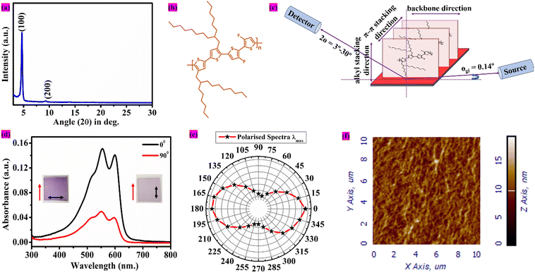
The polymer P4T2F-HD was obtained from Ossilla Co., and its chemical structure is given in Fig. 3(b). This compound, with its molecular structure represented by the formula (C48H70F2S4)n, exhibits an average molecular weight of approximately 44 kDa and is catalogued under the batch number M23481A. P4T2F-HD stands out due to its exceptional processability and resilience to environmental challenges, positioning it as an ideal choice for various applications. Furthermore, essential reagents such as ethylene glycol, glycerol, and chloroform were acquired from Sigma Aldrich, while a 300 nm-thick silicon dioxide (SiO2)-coated Si wafer, was sourced from Global Nanotech Ltd.2.2. Thin film and OFET fabrication
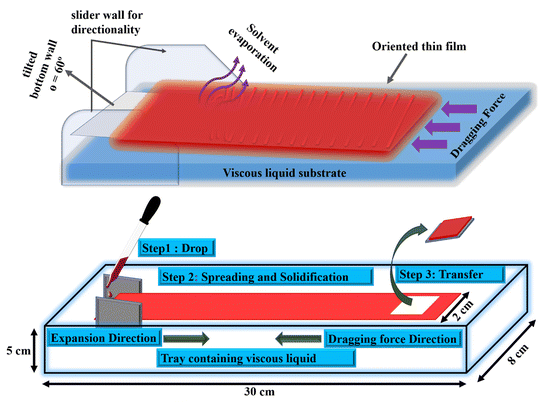
The P4T2F-HD ink was prepared using anhydrous chloroform for a 15 mg ml−1 concentration. It was heated to 50 °C and stirred for one hour to ensure a homogeneous solution. The process included ultrasonication for 10 minutes in a Yamato Branson ultrasonic bath, an essential step intended to encourage the formation of aggregates in the solution. For the fabrication of UFTM thin films, a precise volume of 10 μl of the conjugated polymer (CP) solution was gently positioned next to a specifically designed slider on the liquid sub-phase. This setup allowed for controlled expansion of the film in one direction, as illustrated in Fig. 1. This technique allowed for the distinct alignment of the polymer chains based on the hydrophobicity levels of their side chains, with CPs having more hydrophobic side chains aligning edge-on and those with less hydrophobic side chains aligning face-on upon deposition on a hydrophilic liquid substrate, specifically ethylene glycol at 40 °C. Once formed at the air–liquid interface, the thin films were moved to their designated substrates and cleaned with methanol to eliminate any residual sub-phase liquid from the fabrication process. Following the cleaning, the films underwent annealing for 10 minutes at 120 °C in a nitrogen-filled atmosphere inside a glove box, followed by a gradual cooling period of 30 minutes. These carefully prepared thin films underwent further characterization. OFETs were fabricated on a highly p-doped Si substrate with dimension of 17 × 18 mm, which had a thickness of 300 nm as shown in Fig. 2(c). The device fabrication began with a thorough cleaning regimen, initially using Hellmanex solution, followed by a series of washes in hot, double-distilled water. Subsequent steps included ultrasonication in acetone and IPA, each for ten-minute intervals, and a drying step involving annealing at 120 °C for half an hour. A plasma cleaning stage was incorporated to enhance the substrate's cleanliness, and for improved hydrophobicity, the substrate was immersed in an ODTS/toluene solution for two hours. The final steps involved rinsing with toluene and a second annealing phase at 80 °C to finalize the hydrophobic surface modification. The carefully prepared thin film was lifted onto the substrate using the UFTM. Following the transfer, annealing step at 120 °C for 30 minutes was conducted to ensure the film's optimal characteristics. A gold layer with 100 nm thickness was thermally evaporated to finalize the device fabrication to create the electrodes. A nickel shadow mask was utilized to accurately define the source-drain channels, which are 50 μm in length and 2.8 mm width. For anisotropy by SHG round shaped electrodes were fabricated as shown in Fig. 2(b).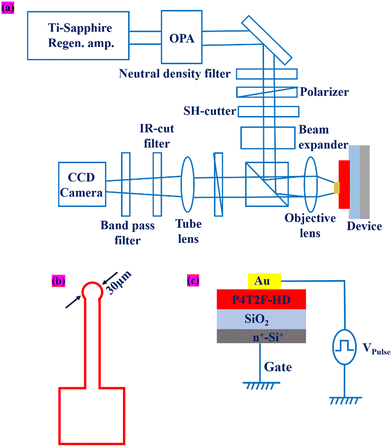 | ||
| Fig. 2 (a) Setup of the optical apparatus for TRM-SHG measurement. (b) Schematic of the round-shaped electrode configuration, (c) schematics of the device structure and the electrical connection. | ||
3. Characterization tools
A suite of sophisticated analytical methodologies was employed to perform a comprehensive examination and characterization of P4T2F-HD thin films. Grazing incidence X-ray diffraction (GIXD) was utilized to examine the crystallographic texture and interlayer spacing of the thin film, employing a Rigaku Smart Lab system with specialized out-of-plane diffraction capabilities. The instrument used Cu Kα radiation and operated at a voltage of 45 kV and a current of 40 mA. The optical attributes of the thin films and their precursor solutions were evaluated through UV-VIS absorption spectroscopy in the absorption configuration, utilizing a Shimadzu UV-2600 spectrophotometer for precise measurements. The polarized absorption spectra of the same sample were recorded at various angles, ranging from 0° to 360°, using a polarizer. The topographical features of the P4T2F-HD surfaces were investigated using atomic force microscopy (AFM) from NT-MDT in Russia, enabling the acquisition of high-resolution images to assess the surface morphology of the films. The electrical properties of the FETs were measured under ambient conditions, at room temperature, with a relative humidity of 50%, in a darkened environment, utilizing a Keithley 2612 source meter for the analysis. Additionally, SHG microscopy was employed as a novel approach to visualize and analyze the anisotropic behavior of charge carriers within the films, offering insights into their directional electronic transport characteristics.In the depicted experimental setup for TRM-SHG, presented in Fig. 2(a), the light source utilized was a femtosecond optical parametric amplifier (OPA, Opera Solo model by Coherent). This OPA was excited by a titanium–sapphire (Ti:sapphire) regenerative amplifier system (Libra model, courtesy of Coherent), renowned for its high stability and precision, which are pivotal for this type of experiment. The laser system operated with an 80-femtosecond pulse duration and a 1 kHz repetition frequency. The OPA's fundamental output, using an objective lens, was accurately focused onto a circular electrode. The SHG signal produced by the sample was then carefully separated from the fundamental light and any extraneous light through a filtering process. This step involved the deployment of infrared-cut and interference filters, indispensable for the SHG signal's isolation from background noise and optical disturbances. The refined SHG signal was subsequently captured and recorded with an advanced, cooled charge-coupled device (CCD) camera (Newton model by Andor), selected for its exceptional sensitivity and minimal noise features, crucial for the detection of weak SH signals.
4. Result and discussion
4.1. Thin film characterization
The out-of-plane X-ray diffraction (XRD) characterization of P4T2F-HD thin films has been conducted to elucidate their molecular orientation. As illustrated in Fig. 3(a), the XRD pattern reveals pronounced diffraction peaks, notably at the (100) and (200) planes, indicating a high degree of crystalline order and uniform stacking of the polymer chains parallel to the film surface. The sharpness and intensity of the (100) peak suggest a strong edge-on orientation, which is associated with efficient charge transport pathways.29 The schematic in Fig. 3(c) depicts the experimental setup for the out-of-plane XRD analysis, highlighting the alignment of the source, the oriented P4T2F-HD polymer film, and the detector. These findings confirm the successful fabrication of highly ordered P4T2F-HD films with a well-defined molecular orientation that is anticipated to contribute to superior electronic performance in organic electronics applications.The thin film of P4T2F-HD, fabricated using the UFTM, was subjected to optical characterization using polarized UV-visible spectroscopy. The absorption band of P4T2F-HD are between 480–630 nm, as depicted in Fig. 3(d). The molecular orientation of the P4T2F-HD film was evaluated using the optical dichroic ratio (DR), a metric derived by examining the UV spectrum under polarized light across various angles. The dichroic ratio typically measures the orientation within the films, DR = A∥/A⊥, where A∥ and A⊥ denote the peak absorbances at λmax parallel and perpendicular to the main chain, respectively.30 The Figure reveals an enhanced orientation from 0 to 90 degrees of polarization. The UV-visible absorption spectra showcased significant anisotropic behavior in the P4T2F-HD films, with a marked peak at λmax, representative of the polymer's main absorption band, displaying distinct intensity fluctuations as the polarization angle shifted from 0° to 360° as shown in Fig. 3(e). Such variance signals the extent of molecular orientation within the film. The DR, deduced from the polarization-dependent absorption, offered a quantifiable anisotropy index, indicating superior alignment along specific axes.
Fig. 3(f) presents an image that confirms the surface roughness and the orientation within a polymer thin film sample. The average roughness measured from the AFM analysis is approximately 1.5 nm, indicating a relatively smooth surface at the nanoscale. This high-resolution topographical mapping provides critical insights into the nanoscale features of the polymer, which are essential for understanding its anisotropic characteristic of the polymer orientation and are crucial for predicting the material's behavior under different orientations.
4.2. Electrical characterization
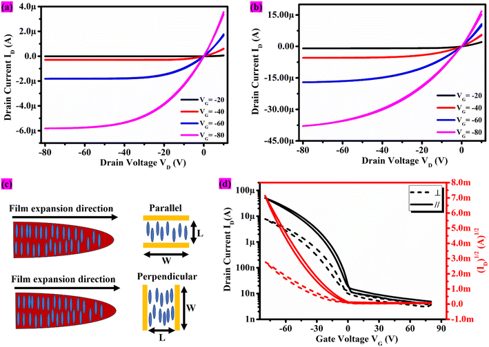
In our exploration, we concentrated on analyzing the impact of anisotropy on the electrical properties of thin films. The emphasis was on understanding the orientation and alignment of molecules within these films and how such structural characteristics affect their electrical properties. Our study examines the phenomena through bottom-gate, top-contact (BGTC) OFETs, where the direction of film spreading is aligned both parallel and perpendicular to the source-to-drain electric field in the channel, as illustrated in Fig. 4(c). For the determination of the saturated field-effect mobility (μsat) and the threshold voltage of the device, we used a method based on fitting a linear equation to the IDS1/2 − VG curve, following the procedure detailed in eqn (1)22 provided. | (1) |
The output characteristics of the parallel and perpendicular aligned film are shown in Fig. 4(a) and (b), respectively, and transfer characteristics are shown in Fig. 4(d). The average field-effect mobility of 30 different devices fabricated in 6 different batches in the saturation regime, calculated for directions parallel (μ∥SAT) and perpendicular (μ⊥SAT) to the film spreading direction, was estimated at 6 × 10⁻² ± 3 × 10⁻³ cm2 V−1 s−1 and 4.01 × 10⁻³ ± 2.2 × 10⁻⁴ cm2 V−1 s−1, respectively. The mobility was approximately an order of magnitude higher in the parallel-oriented devices compared to the perpendicular-oriented ones. The alignment of polymer chains plays a crucial role in the performance and mobility of OFETs. Proper alignment of these chains facilitates efficient charge carrier transport along the backbone of the polymer, enhancing the mobility of the OFETs. This is because the molecular orbitals of the polymer chains overlap better when the chains are well-aligned, allowing for easier movement of charge carriers. When fabricating OFETs, the orientation of the thin film relative to the direction of film expansion significantly influences the device's charge carrier mobility. Devices fabricated with their active layer oriented parallel to the film expansion direction tend to exhibit higher mobility. This occurs as the polymer chains achieve greater uniformity in alignment perpendicular to the direction of film expansion, which facilitates efficient charge transport along the polymer backbone. This alignment minimizes the scattering of charge carriers, thus improving mobility. To verify the orientation of the thin film and the alignment of the polymer chains, TRM-SHG measurements were performed. This technique provides detailed understanding of how molecular alignment affects OFET performance, contributing to the development of high-mobility organic electronic devices.
4.3. SHG measurement
To elucidate the directional charge transport in thin films, we employed a cutting-edge technique known as TRM-SHG, which is adept at mapping the vectorial pathways of carrier movement within films of organic semiconductors.28,31,32 Conventional methods like I–V curve tracing and time-of-flight (TOF) measurements provide valuable data on mobility anisotropy; however, they lack the angular resolution needed to pinpoint the exact directions of highest and lowest carrier mobility due to their inherent limited angular resolution.33,34 TRM-SHG overcomes this limitation by offering a comprehensive view of carrier mobility, enabling precise identification of directions with both superior and inferior mobility, along with their magnitude, directly from the captured images.35 Furthermore, TRM-SHG provides an in-depth analysis of the transport phenomenon, offering direct evaluation of the inherent anisotropy of mobility and the corresponding activation energies.36 The investigation of carrier distribution in thin film devices was conducted using the electric field-induced SHG (EFISHG) technique. When a static electric field E(0) is applied, and the material is concurrently irradiated with a powerful laser beam, a second-order nonlinear polarization response is induced.37 This response is described by the following eqn (2):| P(2ω) = ∈0χ(2)E(ω)E(ω) + ∈0χ(3)E(0)E(ω)E(ω) | (2) |
In our exploration of TRM-SHG analysis, we chose a wavelength of 1120 nm for the incident light, capturing the SHG signal at 560 nm. Fig. 5(b) clearly displays the SHG images from the P4T2F-HD, with a prominent SHG signal concentrated around the central electrode, indicating its origination from the P4T2F-HD layer exclusively. A white marker outlines the edge of the electrode for visual clarity. For these images, a pulsed voltage of 120 V was applied to the circular electrode and the bottom electrode was connected to ground. The captured image reflects a specific instant, 100 nanoseconds after carrier injection, offering a snapshot of carrier distribution at that moment. Our analysis shows that the carriers disperse in various directions at differing speeds, as illustrated in Fig. 5(b), with arrows marking the fastest and slowest carrier paths. This in-plane inhomogeneity in carrier motion is related to the one-dimensional character of excitons in π-conjugated polymers, where the maximum absorption is in alignment with the polymer's primary chain or the film's orientation. It was observed that the carrier mobility is highest along the primary chain direction in the aligned P4T2F-HD film. This mobility is calculated using eqn (3), which describes the directional movement of carriers within the substance.
 | (3) |
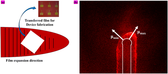 | ||
| Fig. 5 (a) Shows the stamped thin film from the orientation thin film, and lines on the thin films show the orientation polymer chains (b) time-resolved SHG image of the device. | ||
In this study, we investigated SHG by modulating the delay time between 0 ns and 500 ns in increments of 100 ns, as illustrated in Fig. 6. The analysis revealed that the initial phase of carrier displacement correlates with the square root of time, indicating a complex transport mechanism that extends beyond mere diffusion, influenced significantly by the spatial charge field as previously discussed. Furthermore, the spatial distribution of carriers emanating from the round-shaped electrode over time suggests a focus on carrier migration through the material rather than just their injection point. To ascertain the orientation of the deposited thin film, we positioned the film at a 45° angle relative to the flow direction, as shown in Fig. 5(a). This orientation was confirmed using SHG imaging performed at various intervals, as shown in Fig. 6. Notably, there was a significant enhancement of charge carrier mobility along the direction of alignment, with decreased activity in directions perpendicular to the film's orientation. This behavior is likely due to the uniform alignment of polymer chains along the expansion direction of the film. Such an alignment enhances charge transport along the polymer backbone by reducing charge carrier scattering, thereby significantly boosting carrier mobility within the thin film.40,41 This disparity underscores the anisotropic nature of charge transport in these materials, suggesting that even minor variations in the fabrication process or molecular alignment could significantly affect transport efficiency. These results clearly demonstrate the substantial impact of molecular orientation on the charge transport properties of P4T2F-HD thin films. The stark contrast in carrier velocities between the maximum and minimum directions emphasizes the crucial role of precise molecular alignment in enhancing the electrical performance of organic semiconductor devices. By carefully adjusting the orientation angle during the fabrication process, we can greatly improve directional charge transport, potentially leading to the development of more efficient and high-performing organic electronic devices. This investigation into the detailed effects of molecular orientation on charge transport provides critical insights for the design and optimization of future organic semiconductor technologies.
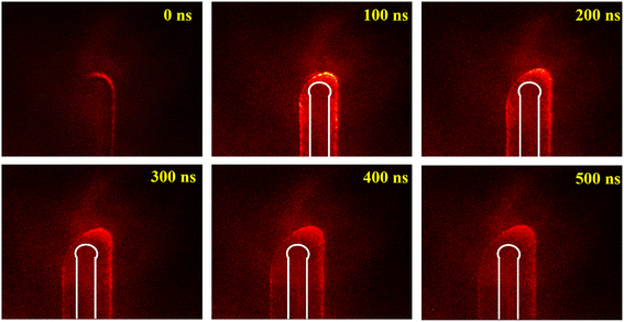 | ||
| Fig. 6 Represents the time-resolved SHG image of the device with different time intervals from 0 to 500 ns. | ||
Conclusion
In conclusion, our investigation into the anisotropic charge transport in highly oriented P4T2F-HD thin films, using both SHG analysis and conventional electrical characterization techniques, has provided substantial insights. We observed a distinct difference in mobility, which was 6 × 10⁻² cm2 V−1 s−1 along the direction parallel to the film orientation and 4.01 × 10⁻³ cm2 V−1 s−1 in the perpendicular direction. SHG analysis further refined our understanding, revealing mobility values of about 0.045 cm2 V−1 s−1 in the maximum direction and 2.1 × 10⁻³ cm2 −1 in the minimum direction. These results highlight the significant influence of molecular orientation on the electrical properties of the films, with a marked disparity in mobility and carrier velocity across different directions. This emphasizes the critical role of directional alignment in enhancing the performance of organic semiconductor devices.Data availability
The data supporting this article were generated through experimental procedures. These data are included in the data availability file; however, this file does not contain any external citations. Additionally, we used Origin software for plotting all the data presented.Author contributions
Radhe Shyam: conceptualization, experimentation and characterization, data analysis, original manuscript writing; Takaaki Manaka: conceptualization, resources, data validation, and manuscript editing; Rajiv Prakash: conceptualization, resources, supervision, and manuscript editing.Conflicts of interest
The authors declare that they have no conflict of interest.Acknowledgements
The authors extend their sincere thanks to the Open Facility Centre (OFC) at TokyoTech for the characterization services provided, which were indispensable for the completion of this work. Radhe shyam wishes to express his gratitude to IIT BHU for awarding him an institute fellowship, which has significantly contributed to the progress of this research.References
- A. R. Murad, A. Iraqi, S. B. Aziz, S. N. Abdullah and M. A. Brza, Conducting polymers for optoelectronic devices and organic solar cells: A review, Polymers, 2020, 12(11), 2627 CrossRef CAS PubMed.
- M. Brinkmann, L. Hartmann, L. Biniek, K. Tremel and N. Kayunkid, Orienting Semi-Conducting π-Conjugated Polymers, Macromol. Rapid Commun., 2014, 35(1), 9–26 CrossRef CAS PubMed.
- P. Tan, H. Wang, F. Xiao, X. Lu, W. Shang and X. Deng, et al., Solution-processable, soft, self-adhesive, and conductive polymer composites for soft electronics, Nat. Commun., 2022, 13(1), 358 CrossRef CAS PubMed.
- J. Huang, J. Du, Z. Cevher, Y. Ren, X. Wu and Y. Chu, Printable and flexible phototransistors based on blend of organic semiconductor and biopolymer, Adv. Funct. Mater., 2017, 27(9), 1604163 CrossRef.
- M. Jaiswal and R. Menon, Polymer electronic materials: a review of charge transport, Polym. Int., 2006, 55(12), 1371–1384 CrossRef CAS.
- Z. Yang, H. Guo, C. Kang and L. Gao, Enhanced gas barrier properties of polymer substrates for flexible OLEDs by adjusting the backbone rigidity and incorporating 2D nanosheets, New J. Chem., 2021, 45(29), 12945–12956 RSC.
- A. A. Husain, W. Z. W. Hasan, S. Shafie, M. N. Hamidon and S. S. Pandey, A review of transparent solar photovoltaic technologies, Renewable Sustainable Energy Rev., 2018, 94, 779–791 CrossRef CAS.
- S. Tiwari, A. K. Singh, L. Joshi, P. Chakrabarti, W. Takashima and K. Kaneto, et al., Poly-3-hexylthiophene based organic field-effect transistor: Detection of low concentration of ammonia, Sens. Actuators, B, 2012, 171, 962–968 CrossRef.
- C. A. Di, G. Yu, Y. Liu and D. Zhu, High-performance organic field-effect transistors: Molecular design, device fabrication, and physical properties, J. Phys. Chem. B, 2007, 111(51), 14083–14096 CrossRef CAS PubMed.
- R. Shyam, S. Jana, T. Manaka and R. Prakash, Development of High-Performance flexible Photodetectors through band engineering and synergistic modulation in P3HT/C3N5 thin film, Sens. Actuators, B, 2024, 136190 CrossRef CAS.
- J.-L. Brédas, J. P. Calbert, F. D. da Silva and J. Cornil, Organic semiconductors: A theoretical characterization of the basic parameters governing charge transport, Proc. Natl. Acad. Sci. U. S. A., 2002, 99(9), 5804–5809 CrossRef PubMed.
- M. V. Jacob, Organic Semiconductors: Past, Present and Future, Electronics, 2014, 3(4), 594–597 CrossRef.
- K. Kim, J. Hong, S. G. Hahm, Y. Rho, T. K. An and S. H. Kim, et al., Facile and microcontrolled blade coating of organic semiconductor blends for uniaxial crystal alignment and reliable flexible organic field-effect transistors, ACS Appl. Mater. Interfaces, 2019, 11(14), 13481–13490 CrossRef CAS PubMed.
- M. Pandey, N. Kumari, S. Nagamatsu and S. S. Pandey, Recent advances in the orientation of conjugated polymers for organic field-effect transistors, J. Mater. Chem. C, 2019, 7(43), 13323–13351 RSC.
- Y. Abe, D. Taguchi, T. Manaka and M. Iwamoto, Study of carrier transport in flexible organic field-effect transistors: Analysis of bending effect and microscopic observation using electric-field-induced optical second-harmonic generation, Thin Solid Films, 2014, 554, 166–169 CrossRef CAS.
- M. Desu, S. Sharma, K.-H. Cheng, Y.-H. Wang, S. Nagamatsu and J.-C. Chen, et al., Controlling the molecular orientation of a novel diketopyrrolopyrrole-based organic conjugated polymer for enhancing the performance of organic field-effect transistors, Org. Electron., 2023, 113, 106691 CrossRef CAS.
- N. Yadav, N. Kumari, Y. Ando, S. S. Pandey and V. Singh, PCPDTBT copolymer based high performance organic phototransistors utilizing improved chain alignment, Opt. Mater., 2021, 113, 110886 CrossRef CAS.
- J. Aneli, G. Zaikov and L. Khananashvili, Effects of mechanical deformations on the structurization and electric conductivity of electric conducting polymer composites, J. Appl. Polym. Sci., 1999, 74(3), 601–621 CrossRef CAS.
- M. S. Mahajan, D. Marathe, S. S. Ghosh, V. Ganesan and J. V. Sali, Changes in in-plane electrical conductivity of PEDOT: PSS thin films due to electric field induced dipolar reorientation, RSC Adv., 2015, 5(105), 86393–86401 RSC.
- V. Chaudhary, R. K. Pandey, R. Prakash, N. Kumar and A. K. Singh, Highly aligned and crystalline poly (3-hexylthiophene) thin films by off-center spin coating for high performance organic field-effect transistors, Synth. Met., 2019, 258, 116221 CrossRef CAS.
- M. Pandey, Y. Sugita, J. Toyoda, S. Katao, R. Abe and Y. Cho, et al., Unidirectionally Aligned Donor–Acceptor Semiconducting Polymers in Floating Films for High-Performance Unipolar n-Channel Organic Transistors, Adv. Electron. Mater., 2023, 9(2), 2201043 CrossRef CAS.
- R. Shyam, S. Jana, T. Manaka and R. Prakash, Template-Assisted Assembly of DPP-TTT over a Hydrophilic Liquid Subphase toward Enhanced Charge Transport in Organic Field-Effect Transistors, ACS Appl. Polym. Mater., 2024, 6(11), 6737–6746 CrossRef CAS.
- S. Sharma, A. K. Vats, M. Pandey, S. Nagamatsu, J.-C. Chen and S. S. Pandey, Unraveling the implications of macromolecular orientation on the planar and vertical charge transport in organic electronic devices, ACS Appl. Polym. Mater., 2022, 4(11), 8315–8323 CrossRef CAS.
- R. K. Pandey, A. S. Tripathi, S. S. Pandey and R. Prakash, Optoelectrical anisotropy in graphene oxide supported polythiophene thin films fabricated by floating film transfer, Carbon, 2019, 147, 252–261 CrossRef CAS.
- E. Mohammadi, C. Zhao, Y. Meng, G. Qu, F. Zhang and X. Zhao, et al., Dynamic-template-directed multiscale assembly for large-area coating of highly-aligned conjugated polymer thin films, Nat. Commun., 2017, 8(1), 16070 CrossRef CAS PubMed.
- S. Sharma, A. K. Vats, L. Tang, F. Kaishan, J. Toyoda and S. Nagamatsu, et al., High field-effect mobility in oriented thin films of DA type semiconducting polymers by engineering stable interfacial system, Chem. Eng. J., 2023, 143932 CrossRef CAS.
- K. Abe, T. Manaka and M. Iwamoto, Direct evaluation of anisotropic carrier mobility in uniaxially aligned polymer semiconductor film by time-resolved microscopic optical second-harmonic generation measurement, J. Phys. D: Appl. Phys., 2016, 50(1), 015103 CrossRef.
- T. Manaka, K. Matsubara, K. Abe and M. Iwamoto, Direct observation of anisotropic carrier transport in organic semiconductor by time-resolved microscopic optical second-harmonic imaging, Appl. Phys. Express, 2013, 6(10), 101601 CrossRef.
- S. Jana, R. K. Pandey and R. Prakash, Evolution of Edge-On Oriented Polymer Films Self-Assembled at the Air–Liquid Interface for High-Performance Electronic Device Applications, ACS Appl. Polym. Mater., 2022, 4(7), 4818–4828 CrossRef CAS.
- A. S. Tripathi, M. Pandey, S. Sadakata, S. Nagamatsu, W. Takashima, S. Hayase and S. S. Pandey, Anisotropic charge transport in highly oriented films of semiconducting polymer prepared by ribbon-shaped floating film, Appl. Phys. Lett., 2018, 112(12), 123301 CrossRef.
- T. Manaka, E. Lim, R. Tamura and M. Iwamoto, Direct imaging of carrier motion in organic transistors by optical second-harmonic generation, Nat. Photonics, 2007, 1(10), 581–584 CrossRef CAS.
- T. Manaka and M. Iwamoto, Optical second-harmonic generation measurement for probing organic device operation, Light: Sci. Appl., 2016, 5(3), e16040 CrossRef CAS PubMed.
- H. Zhong, Z. Zhang, H. Xu, C. Qiu and L. M. Peng, Comparison of mobility extraction methods based on field-effect measurements for graphene, AIP Adv., 2015, 5(5), 057136 CrossRef.
- Y. Zhou, X. Wang and A. Dodabalapur, Accurate Field-Effect Mobility and Threshold Voltage Estimation for Thin-Film Transistors with Gate-Voltage-Dependent Mobility in Linear Region, Adv. Electron. Mater., 2023, 9(2), 2200786 CrossRef CAS.
- T. Manaka, F. Liu, M. Weis and M. Iwamoto, Studying transient carrier behaviors in pentacene field effect transistors using visualized electric field migration, J. Phys. Chem. C, 2009, 113(23), 10279–10284 CrossRef CAS.
- M. Iwamoto, T. Manaka and D. Taguchi, Probing and modeling of carrier motion in organic devices by electric-field-induced optical second-harmonic generation, Jpn. J. Appl. Phys., 2014, 53(10), 100101 CrossRef.
- R. W. Terhune, P. D. Maker and G. M. Savage, Optical harmonic generation in calcite, Phys. Rev. Lett., 1962, 8, 404–406 CrossRef CAS.
- A. Ovchinnikov, O. Chefonov, E. Mishina and M. Agranat, Second harmonic generation in the bulk of silicon induced by an electric field of a high power terahertz pulse, Sci. Rep., 2019, 9(1), 9753 CrossRef CAS PubMed.
- T. Manaka, F. Liu, M. Weis and M. Iwamoto, Influence of traps on transient electric field and mobility evaluation in organic field-effect transistors, J. Appl. Phys., 2010, 107(4), 043712 CrossRef.
- S. Fratini, M. Nikolka, A. Salleo, G. Schweicher and H. Sirringhaus, Charge transport in high-mobility conjugated polymers and molecular semiconductors, Nat. Mater., 2020, 19(5), 491–502 CrossRef CAS PubMed.
- M. Chang, G. T. Lim, B. Park and E. Reichmanis, Control of molecular ordering, alignment, and charge transport in solution-processed conjugated polymer thin films, Polymers, 2017, 9(6), 212 CrossRef PubMed.
| This journal is © The Royal Society of Chemistry 2024 |

