 Open Access Article
Creative Commons Attribution 3.0 Unported Licence
Band-gap engineering in methylammonium bismuth bromide perovskites for less-toxic perovskite solar cells†
Samuel R.
Pering
 *a,
Hunaynah
Abdulgafar‡
a,
Madeleine
Mudd
a,
Keith
Yendall
b,
Mustafa
Togay
c and
Mark R.J.
Elsegood
 d
d
aDepartment of Materials, Loughborough University, Loughborough, LE11 3TU, UK. E-mail: s.r.pering@lboro.ac.uk
bLoughborough Materials Characterisation Centre, Loughborough, LE11 3TU, UK
cCREST, Loughborough University, Loughborough, LE11 3TU, UK
dDepartment of Chemistry, Loughborough University, Loughborough, LE11 3TU, UK
First published on 29th November 2023
Abstract
Bismuth-based perovskites could be a viable and efficient alternative to lead-based perovskite materials. To widen possible applications, it is necessary to be able to alter the band gap of the absorber material (i.e. for water splitting or multijunction cells). In this work we show the possibility of colour-management in methylammonium bismuth halide perovskites. When synthesised using DMSO, methylammonium bismuth bromide is characterised and identified as possessing a zero-dimensional perovskite type structure with a formula of MA3BiBr6 DMSO solvate, and a band gap of 2.51 eV. An increasing mole fraction of iodide ions into methylammonium bismuth bromide is shown to produce a single-phase with a decreasing band gap, with an associated colour change from yellow (2.51 eV) for methylammonium bismuth bromide to red (1.88 eV) for methylammonium bismuth iodide. The methylammonium bismuth iodide structure is tolerant to high degrees of bromide substitution, up to 40%, before significant effects in band gap or morphology are observed. Halide substitution was also found to aid thin-film stability over 10 weeks in air. The insights obtained from this study could provide additional stability at a reduced cost to lead-free bismuth halide perovskite materials.
Introduction
Renewable, low-carbon energy sources are vital for reducing societal dependence on fossil fuels and mitigating the effects of carbon emissions. Reducing both start-up and implementation costs is key to the uptake of new technologies to decrease our environmental impact. With increasingly reducing energy-payback times, solar power has become an attractive alternative energy source. Its flexibility, finding use in both >100 MW solar farms and smaller rooftop arrays means that it is accessible to a range of applications. New materials can widen these possibilities further for building-integration, such as photovoltaic windows.1,2In the past 10 years, perovskite-structured photovoltaic materials have established themselves as an exciting new opportunity for solar technologies.3 Abundant starting materials and simple processing methods are significant advantages of these materials; the latter enabling the fabrication of flexible perovskite solar cells (PSC).4–8 From a 3% efficient cell reported for the original material, methylammonium lead iodide (MAPI) in 2009, the record efficiency for perovskite solar cells now lies at over 25%, competitive with commercially established solar cell technologies such as silicon.3,9 A major part of improving device performance was tailoring the constituents of the perovskite by the inclusion of additives at the A or X-site (from an ABX3 general structure).10–12 This could involve small ions such as Br−, with halide mixing proving to improve stability and aid in the control of the material band-gap.13–15 An easily controlled band gap has opened the possibility of implementing perovskite materials in multijunction cells, as complementary band gaps to those of other materials for maximum absorption can be designed.16,17 Additionally the incorporation of larger cations can improve material stability, for example the most stable cells use longer chain organic compounds that form a more stable 2D perovskite structure.18–20
However, the long-term stability of perovskite solar cell devices has been significantly less than commercially established technologies, which is further complicated by the potential release into the environment of the toxic element lead.21–25 The exploration of lead-free materials is therefore important to further development of perovskite solar cell technology. Recently lead-free perovskite solar cells have seen significant progress, albeit with lower efficiencies than lead-based analogues.26,27 The next element up in group 14, tin, is the most widely analysed alternative, but its toxicity, efficiency, and stability have not shown improvements over lead.28,29
Recently, bismuth has been employed as a lead replacement in the B-site; its most common oxidation state of +3 has led to a variance in structures, for example double perovskites are formed when used in conjunction with a +1 ion such as silver.30–32 Silver–bismuth double perovskite solar cells have reached efficiencies of over 2% in thin-film solar cells, and over 4% when the perovskite is converted into quantum dot form.33,34 Functioning solar cells can also be produced when bismuth is used as the solitary B-site cation, although efficiencies remain mostly below 1%, with the highest of these obtained with caesium as the A-site cation.35–38 Improving the performance of A3Bi2X9 materials is therefore paramount to establish bismuth as a potential competitor to lead. For example, by using a two-step deposition method, cells exhibiting 3.17% efficiency for a methylammonium bismuth iodide cell have been produced.39
Band gap engineering has been used throughout perovskite solar cell research to improve device performance, and can also be used to form an ideal material for certain applications, e.g. in tandem cells or for building integrated photovoltaics, and halide mixing has been demonstrated to be an effective way of altering the band-gap/colour of a material.17,40–42 In this article we introduce a previously unreported structure of the material methylammonium bismuth bromide, including single crystal data. The effect of halide mixing on bismuth perovskites is then examined, using various ratios of iodide to bromide from MA3Bi2I9 to MA3Bi2Br9, analysing the structural, optical and morphological effects to both assess any improvements in material performance, and observe any similarities to band-gap engineering in lead-based perovskites.
Results & discussion
Methylammonium bismuth bromide
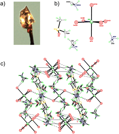
Single crystal analysis determined that the structure obtained was a DMSO solvate crystal structure. Large, single, crystals of methylammonium bismuth bromide dimethyl sulfoxide solvate, 1, were grown using a 2![[thin space (1/6-em)]](https://www.rsc.org/images/entities/char_2009.gif) :
:![[thin space (1/6-em)]](https://www.rsc.org/images/entities/char_2009.gif) 1 ratio of methylammonium bromide:bismuth bromide in a mixed solvent of γ-butyrolactone and dimethyl sulfoxide, using a solvent evaporation method. An image of the crystal fragment used for the data collection is shown in Fig. 1a. Fig. 1b and c show the formula unit and packing motifs in the crystal structure of 1. Fig. S1 and S2 (ESI†) show packing plots in different orientations. All crystal data is in Table S2 (ESI†).
1 ratio of methylammonium bromide:bismuth bromide in a mixed solvent of γ-butyrolactone and dimethyl sulfoxide, using a solvent evaporation method. An image of the crystal fragment used for the data collection is shown in Fig. 1a. Fig. 1b and c show the formula unit and packing motifs in the crystal structure of 1. Fig. S1 and S2 (ESI†) show packing plots in different orientations. All crystal data is in Table S2 (ESI†).
[(BiBr63−)(H3CNH3+)3]·2((CH3)2SO) (1) is the moiety formula for the crystallised material, and one quarter of this represents the asymmetric unit. The DMSO and methylammonium cations were substantially disordered. In the case of the methylammonium cations the two ends were positionally disordered i.e. C/N swap places. Layers of cations and anions are linked via an extensive network of H-bonds involving all structural components. The BiBr63− anions are almost perfectly octahedral and do not connect with each other (0D).
The monoclinic, C2/m structure characterised from these experiments is not a typically observed perovskite structure, nor is it the same as previous characterisations of methylammonium bismuth bromide. A study by Djokic et al. produced a more expected MA3Bi2Br9 material, with 2D layered structure belonging to the space group P![[3 with combining macron]](https://www.rsc.org/images/entities/char_0033_0304.gif) m1, similar to previous studies on bismuth and antimony halide perovskites.43,44 It is also unlike the crystal structure of methylammonium bismuth iodide, which usually possesses a structure in which two face-sharing octahedra form the main part of the repeating unit.45 This difference is likely due to the synthesis method of the single crystals, a slow, solvent evaporation-based method that allows plenty of time for the crystallisation of the material to include the DMSO solvent.
m1, similar to previous studies on bismuth and antimony halide perovskites.43,44 It is also unlike the crystal structure of methylammonium bismuth iodide, which usually possesses a structure in which two face-sharing octahedra form the main part of the repeating unit.45 This difference is likely due to the synthesis method of the single crystals, a slow, solvent evaporation-based method that allows plenty of time for the crystallisation of the material to include the DMSO solvent.
Halide mixing in bismuth halide perovskites
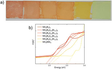
To investigate the effect of halide mixing, powders of methylammonium bismuth halide with different ratios of iodide to bromide were prepared for powder X-ray diffraction (PXRD) analysis. These were prepared with an increasing molar ratio of bromide by 0.2 in each solution, to provide a broad picture of the potential band-gap engineering available in bismuth-based perovskite materials. An immediate colour difference in the powders was observed, from a deep red for MA3Bi2I9, through shades of orange to yellow in MA3BiBr6 (Fig. 3a displays this colour difference in the thin-films). This echoes the trends shown by lead halide perovskites, in which increasing the proportion of bromide in the material increases the band gap.13 The PXRD results obtained from the powders are shown in Fig. 2 and a comparison with the starting materials for the 100% iodide and 100% bromide material are included in Fig. S3 (ESI†). These show distinct peaks, separate from those of the starting materials, however a lack of complete conversion is observed. The diffractograms show no obvious peak separation, so a single phase of mixed halide methylammonium bismuth perovskite is produced in each case. An enhanced image tracking the (1,0,2) peak46 of MA3Bi2I9 shows a gradual shift to higher 2θ values as the proportion of bromide increases, suggesting that the inclusion of the smaller bromide ion is reducing the overall size of the unit cell (see Fig. 2b).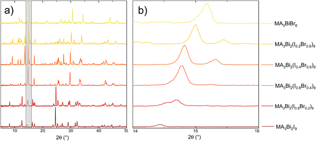 | ||
| Fig. 2 Powder X-ray diffractograms (normalised) for methylammonium bismuth halide with varying iodide:bromide ratio: (a) full diffractogram, and (b) zoomed-in image of shaded area, tracking the (1,0,2)46 peak. | ||
There is little change in the overall diffractogram from MA3Bi2I9 to MA2Bi2(I0.8Br0.2)9 suggesting that the structure is potentially tolerant to high levels of substitution. As BiBr3 can be significantly cheaper than BiI3 (at lower purities, BiBr3: £175/100 g (≥ 98%) BiI3: £270/100 g (99%) (Merck) in May 2023), these findings could greatly reduce the cost of bismuth-based perovskite solar cells, if the other major properties such as band gap and device efficiency can be maintained at these substitution levels. At 40% bromide substitution and above, there is a more significant shift in peak positions, this more pronounced change matching the change in the colour of the powders.
A single-step spin-coating method was employed to produce thin-films for analysis to reduce procedural complexity and to ensure observed morphology differences are due to the material composition as opposed to deposition method. An image of the thin films is shown in Fig. 3a. UV/Vis analysis of these films shows that the band gap has been successfully altered through varying the halide composition (Fig. 3b).
Analysis of the band-gap extracted from linear fitting of the first visible transition in the diffuse reflectance spectroscopy echoes the trends obtained from PXRD measurements; i.e. the material is tolerant to high levels of bromide substitution without significant change (Fig. S4, ESI†). Table 1 below shows the band gaps extracted from UV/Vis analysis.
| Material | Band gap (eV) |
|---|---|
| MA3Bi2I9 | 1.88 |
| MA3Bi2(I0.8Br0.2)9 | 1.91 |
| MA3Bi2(I0.6Br0.4)9 | 1.93 |
| MA3Bi2(I0.4Br0.6)9 | 1.98 |
| MA3Bi2(I0.8Br0.2)9 | 2.08 |
| MA3BiBr6 | 2.51 |
For MA3Bi2I9 a band gap of 1.88 eV is obtained, which is consistent with previously reported results.46–48 A slight shift is seen at low percentages of bromide substitution, however as the percentage of bromide in the lattice increases further, there is a starker change in band gap. MA3Bi2(I0.4Br0.6)9 possesses a band gap of 1.98 eV, increasing to 2.08 eV for MA3Bi2(I0.8Br0.2)9. Finally, the 100% Br-containing material has a measured band gap of 2.51 eV. The UV/Vis data establishes that the band-gap of methylammonium bismuth halide perovskites can be controlled through halide substitution, a property that could prove useful for their deployment as a top cell in multijunction solar cells. Compared with methylammonium lead iodide perovskites, methylammonium bismuth iodide requires greater bromide substitution to enact similar degrees of band gap shift.13 A plot of bromide mole fraction against band gap (Fig. S4b, ESI†) produces a curve which appears to show an exponential trend. To test this trend an additional sample was made and measured with 90% bromide (Fig. S4c and d, ESI†). The band gap for MA3Bi2(I0.1Br0.9)9 was measured at 2.18 eV, which fits with the observed trend, and this is likely due to the significant shifts in crystalline structure at higher mole fractions of bromide as seen in the PXRD measurements.
The stability of the thin-films when left in atmospheric conditions was observed over 10 weeks using both XRD (Fig. 4) and UV/Vis (Fig. S6, ESI†). Firstly, the thin-film XRD shows significantly less disorder than the powder, and for all ratios of iodide/bromide appears to be relatively stable throughout the 10 week period, with little change in the major peaks. Interestingly in the first few weeks for MA3Bi2I9 (100% iodide on Fig. 4), there is a split peak at ∼12.5° highlighted in Fig. S6 (ESI†). This suggests that there are two competing phases within the material, which also appears as two separate absorbance changes in the UV/Vis spectra (Fig. S6, ESI†). This apparent phase separation disappears after 4 weeks in both the XRD and UV/Vis suggesting that a single, dominant phase is present. However, in the UV/Vis this is manifested as an increase in the initial band-gap, meaning that less overall light is absorbed. This will likely have implications for device performance, and therefore these phases should be explored in more detail to determine the origin and if it is possible to isolate and maintain the lower band gap phase. This splitting does not occur in any of the mixed iodide:bromide samples. Additionally, there is the appearance over time of a peak at ∼10°, attributed to the methylammonium halide starting material, suggesting material degradation. This is significantly more pronounced in the pure bromide and iodide samples than the mixed halides. An increase in phase stability from halide mixing has also been observed in lead-based perovskites.13,14 These results suggest that halide-mixing could also be a useful tool for bismuth-based perovskites to improve both phase stability and long-term stability. An additional factor is that at low bromide loading the impact on band gap is minimal for a potential increase in long-term stability.
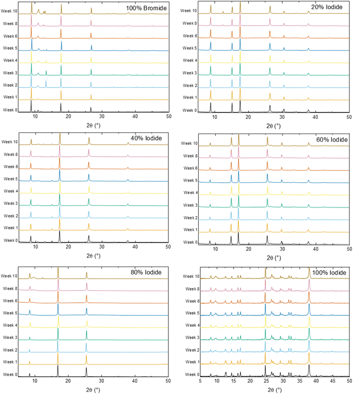 | ||
| Fig. 4 10 week stability study of thin-films through X-ray diffraction. Graph headings correspond to the proportion of iodide or bromide in the sample. | ||
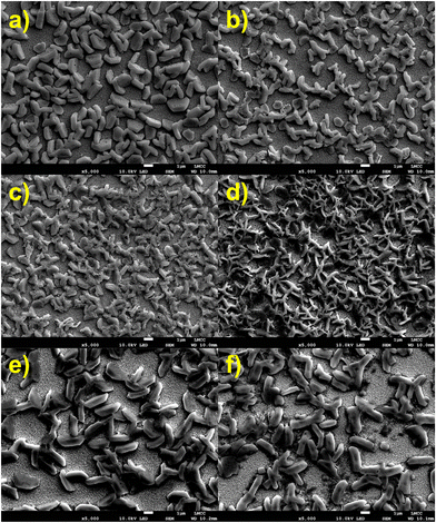
Thin-film morphology was analysed in closer detail using both SEM (Fig. 5 and Fig. S7, ESI†) and AFM (Fig. S8, ESI†) analysis. All films show high surface roughness and a film thickness of between 700 nm to 1 μm, with low surface coverage. For MA3Bi2I9 (Fig. 5a and Fig. S7a, ESI†) flat grains of 1 μm length populate the surface. Films containing 20% and 40% bromide show similar morphologies, and as the proportion of bromide increases further the grains become more rod-like and increase in size (Fig. 5d, e and Fig. S7c–e, ESI†) towards the large, >2 μm size grains that form MA3Bi2Br9. Improving the film morphology of these less-toxic perovskite materials is vital for performance, and should be the subject of further study.
Methylammonium bismuth halide solar cells were fabricated, using polyethylenedioxythiophene:polystyrene sulfonate (PEDOT:PSS) as the hole-transport material and phenyl-C61-butyric acid methyl ester (PCBM) as the electron transport material (Fig. S9 and S10, ESI†). These materials were chosen as they had the simplest fabrication procedures and lowest cost, to maintain the key advantage of simple processing that makes perovskite solar cells attractive. Previous studies looking at MA3Bi2I9 solar cells produced devices with efficiencies of up to 3.17%.36,39,46,49 6 devices were fabricated for each material, with few showing measurable efficiency. The new material MA3BiBr6 exhibited some, albeit minimal photovoltaic activity, in the range of pA cm−2JSC and <0.05 V VOC displayed in Fig. S9f (ESI†). Similar performance was observed across the halide substitution range (Fig. S10, shown alongside dark measurements, ESI†), therefore direct comparisons of the effects of halide mixing on methylammonium bismuth halide solar cells are not possible in this case. This likely has multiple causes: the poor film coverage, uneven film morphology, and zero-dimensional crystal structure, particularly of the MA3BiBr6 materials leading to inefficient charge transport. Improving the morphology of MA3Bi2(I1−xBrx)9 could lead to improved performance at a reduced cost compared with MA3Bi2I9. Other solvents to DMSO should be explored, as the formation of the DMSO solvate crystal into a zero-dimensional structure, as opposed to the previously reported 3-D crystal structures, likely hampers performance.43,44
Conclusions
The crystal structure of the new material methylammonium bismuth bromide dimethylsulfoxide solvate is reported, which shows a zero-dimensional, monoclinic C2/m structure. Methylammonium bismuth halide perovskites are then studied through halide mixing to explore the effects on band-gap and structure. MA3Bi2I9 displays a high tolerance to halide mixing on structure and band gap, which show small changes at bromide substitutions of <40%. Halide substitution has been shown to improve the stability of the materials over 10 weeks in air, suggesting that, this could be a method to increase material lifetime whilst not compromising on band gap. This report contains the first attempted synthesis of a methylammonium bismuth bromide solar cell, which recorded minimal photovoltaic activity; this is attributed to film morphology and the zero-dimensional crystal structure obtained through the fabrication route chosen. Further refinement of the synthesis procedure including analysis of other solvent systems to improve the film morphology of the mixed halide materials and allow solvate-free crystallisation, could lead to cheaper, more sustainable, lead-free perovskite materials.Author contributions
SRP: conceptualisation, funding acquisition, project administration, methodology, supervision, writing – original draft. HA, MM, KY, MT & ME data curation, formal analysis, investigation, resources and writing – review and editing. ME – crystallographic analysis.Conflicts of interest
There are no conflicts to declare.Acknowledgements
We thank the EPSRC UK National Crystallography Service at the University of Southampton for the collection of the crystallographic data for 1.46 SRP thanks the University of Loughborough for funding.References
- M. Batmunkh, Y. L. Zhong and H. Zhao, Adv. Mater., 2020, 2000631 CrossRef CAS PubMed.
- L. Shen, H. Yip, F. Gao and L. Ding, Sci. Bull., 2020, 65, 980–982 CrossRef CAS PubMed.
- A. Kojima, K. Teshima, Y. Shirai and T. Miyasaka, J. Am. Chem. Soc., 2009, 131, 6050–6051 CrossRef CAS PubMed.
- J. Burschka, N. Pellet, S.-J. Moon, R. Humphry-Baker, P. Gao, M. K. Nazeeruddin and M. Grätzel, Nature, 2013, 499, 316–319 CrossRef CAS PubMed.
- N. K. Noel, S. N. Habisreutinger, B. Wenger, M. T. Klug, M. T. Horantner, M. B. Johnston, R. J. Nicholas, D. T. Moore and H. J. Snaith, Energy Environ. Sci., 2017, 10, 145–152 RSC.
- L. Chao, L. Pengwei, G. Hao, Z. Yiqiang, L. Fengyu, S. Yanlin, S. Guosheng, M. Nripan and X. Guichuan, Sol. RRL, 2018, 2, 1700217 CrossRef.
- K. Hwang, Y. S. Jung, Y. J. Heo, F. H. Scholes, S. E. Watkins, J. Subbiah, D. J. Jones, D. Y. Kim and D. Vak, Adv. Mater., 2015, 27, 1241–1247 CrossRef CAS PubMed.
- X. Yin, P. Chen, M. Que, Y. Xing, W. Que, C. Niu and J. Shao, ACS Nano, 2016, 10, 3630–3636 CrossRef CAS PubMed.
- M. A. Green, E. D. Dunlop, J. Hohl-Ebinger, M. Yoshita, N. Kopidakis and A. W. Y. Ho-Baillie, Prog. Photovoltaics Res. Appl., 2020, 28, 3–15 CrossRef.
- C. Yi, J. Luo, S. Meloni, A. Boziki, N. Ashari-Astani, C. Gratzel, S. M. Zakeeruddin, U. Rothlisberger and M. Gratzel, Energy Environ. Sci., 2016, 9, 656–662 RSC.
- O. J. Weber, B. Charles and M. T. Weller, J. Mater. Chem. A, 2016, 4, 15375–15382 RSC.
- G. R. Berdiyorov, F. El-Mellouhi, M. E. Madjet, F. H. Alharbi, F. M. Peeters and S. Kais, Sol. Energy Mater. Sol. Cells, 2015, 1–9 Search PubMed.
- J. H. Noh, S. H. Im, J. H. Heo, T. N. Mandal and S. Il Seok, Nano Lett., 2013, 13, 1764–1769 CrossRef CAS PubMed.
- R. García-Rodríguez, D. Ferdani, S. Pering, P. J. Baker and P. J. Cameron, J. Mater. Chem. A, 2019, 7, 22604–22614 RSC.
- M. Saliba, T. Matsui, J.-Y. Seo, K. Domanski, J.-P. Correa-Baena, M. K. Nazeeruddin, S. M. Zakeeruddin, W. Tress, A. Abate, A. Hagfeldt and M. Grätzel, Energy Environ. Sci., 2016, 9, 1989 RSC.
- D. P. McMeekin, G. Sadoughi, W. Rehman, G. E. Eperon, M. Saliba, M. T. Horantner, A. Haghighirad, N. Sakai, L. Korte, B. Rech, M. B. Johnston, L. M. Herz and H. J. Snaith, Science, 2016, 351, 151–155 CrossRef CAS PubMed.
- T. Moot, J. Werner, G. E. Eperon, K. Zhu, J. J. Berry, M. D. McGehee and J. M. Luther, Adv. Mater., 2020, 2003312 CrossRef CAS PubMed.
- N. De Marco, H. Zhou, Q. Chen, P. Sun, Z. Liu, L. Meng, E.-P. Yao, Y. Liu, A. Schiffer and Y. Yang, Nano Lett., 2016, 16, 1009–1016 CrossRef PubMed.
- S. R. Pering, W. Deng, J. R. Troughton, P. S. Kubiak, D. Ghosh, R. G. Niemann, F. Brivio, F. E. Jeffrey, A. B. Walker, M. S. Islam, T. M. Watson, P. R. Raithby, A. L. Johnson, S. E. Lewis and P. J. Cameron, J. Mater. Chem. A, 2017, 5, 20658–20665 RSC.
- G. Grancini, C. Roldán-Carmona, I. Zimmermann, E. Mosconi, X. Lee, D. Martineau, S. Narbey, F. Oswald, F. De Angelis, M. Graetzel and M. K. Nazeeruddin, Nat. Commun., 2017, 8, 15684 CrossRef CAS PubMed.
- Y. Y. Zhang, S. Chen, P. Xu, H. Xiang, X. G. Gong, A. Walsh and S. H. Wei, Chin. Phys. Lett., 2018, 35, 036104 CrossRef.
- C. Tian, E. Castro, T. Wang, G. Betancourt-Solis, G. Rodriguez and L. Echegoyen, ACS Appl. Mater. Interfaces, 2016, 8, 31426–31432 CrossRef CAS PubMed.
- J. Li, H.-L. Cao, W.-B. Jiao, Q. Wang, M. Wei, I. Cantone, J. Lü and A. Abate, Nat. Commun., 2020, 11, 310 CrossRef CAS PubMed.
- P. Su, Y. Liu, J. Zhang, C. Chen, B. Yang, C. Zhang and X. Zhao, J. Phys. Chem. Lett., 2020, 11, 2812–2817 CrossRef CAS PubMed.
- Y. Zhai, Z. Wang, G. Wang, W. J. G. M. Peijnenburg and M. G. Vijver, Chemosphere, 2020, 249, 126564 CrossRef CAS PubMed.
- T. Miyasaka, A. Kulkarni, G. M. Kim, S. Öz and A. K. Jena, Adv. Energy Mater., 2019, 0, 1902500 Search PubMed.
- S. F. Hoefler, G. Trimmel and T. Rath, Monatsh. Chem., 2017, 148, 795–826 CrossRef CAS PubMed.
- N. K. Noel, S. D. Stranks, A. Abate, C. Wehrenfennig, S. Guarnera, A.-A. Haghighirad, A. Sadhanala, G. E. Eperon, S. K. Pathak, M. B. Johnston, A. Petrozza, L. M. Herz and H. J. Snaith, Energy Environ. Sci., 2014, 7, 3061–3068 RSC.
- A. Babayigit, D. Duy Thanh, A. Ethirajan, J. Manca, M. Muller, H.-G. Boyen and B. Conings, Sci. Rep., 2016, 6, 18721 CrossRef CAS PubMed.
- D. E. Lee, S. Y. Kim and H. W. Jang, J. Korean Ceram. Soc., 2020, 57(5), 455–479 CrossRef CAS.
- G. Volonakis, M. R. Filip, A. A. Haghighirad, N. Sakai, B. Wenger, H. J. Snaith and F. Giustino, J. Phys. Chem. Lett., 2016, 7, 1254–1259 CrossRef CAS PubMed.
- A. H. Slavney, T. Hu, A. M. Lindenberg and H. I. Karunadasa, J. Am. Chem. Soc., 2016, 138, 2138–2141 CrossRef CAS PubMed.
- B. Ghosh, B. Wu, X. Guo, P. C. Harikesh, R. A. John, T. Baikie, Arramel, A. T. S. Wee, C. Guet, T. C. Sum, S. Mhaisalkar and N. Mathews, Adv. Energy Mater., 2018, 8, 1802051 CrossRef.
- S. M. Jain, T. Edvinsson and J. R. Durrant, Commun. Chem., 2019, 2, 91 CrossRef.
- R. L. Z. Hoye, R. E. Brandt, A. Osherov, V. Stevanovic, S. D. Stranks, M. W. B. Wilson, H. Kim, A. J. Akey, J. D. Perkins, R. C. Kurchin, J. R. Poindexter, E. N. Wang, M. G. Bawendi, V. Bulovic and T. Buonassisi, Chem. – Eur. J., 2016, 22, 2605–2610 CrossRef CAS PubMed.
- B. W. Park, B. Philippe, X. Zhang, H. Rensmo, G. Boschloo and E. M. J. Johansson, Adv. Mater., 2015, 27, 6806–6813 CrossRef CAS PubMed.
- R. Waykar, A. Bhorde, S. Nair, S. Pandharkar, B. Gabhale, R. Aher, S. Rondiya, A. Waghmare, V. Doiphode, A. Punde, P. Vairale, M. Prasad and S. Jadkar, J. Phys. Chem. Solids, 2020, 146, 109608 CrossRef CAS.
- K. Ahmad, P. Kumar, H. Kim and S. M. Mobin, ChemNanoMat, 2022, 8, e202200061 CrossRef CAS.
- S. M. Jain, D. Phuyal, M. L. Davies, M. Li, B. Philippe, C. De Castro, Z. Qiu, J. Kim, T. Watson, W. C. Tsoi, O. Karis, H. Rensmo, G. Boschloo, T. Edvinsson and J. R. Durrant, Nano Energy, 2018, 49, 614–624 CrossRef CAS.
- E. Pulli, E. Rozzi and F. Bella, Energy Convers. Manage., 2020, 219, 112982 CrossRef.
- M. L. Davies, M. Carnie, P. J. Holliman, A. Connell, P. Douglas, T. Watson, C. Charbonneau, J. Troughton and D. Worsley, Mater. Res. Innovations, 2014, 18, 482–485 CrossRef CAS.
- B.-B. Yu, M. Liao, J. Yang, W. Chen, Y. Zhu, X. Zhang, T. Duan, W. Yao, S.-H. Wei and Z. He, J. Mater. Chem. A, 2019, 7, 8818–8825 RSC.
- V. Djokić, P. Andričević, M. Kollár, A. Ciers, A. Arakcheeva, M. Vasiljević, D. Damjanović, L. Forró, E. Horváth and T. Ivšić, Crystals, 2022, 12 Search PubMed.
- B. Saparov, F. Hong, J.-P. Sun, H.-S. Duan, W. Meng, S. Cameron, I. G. Hill, Y. Yan and D. B. Mitzi, Chem. Mater., 2015, 27, 5622–5632 CrossRef CAS.
- K. Eckhardt, V. Bon, J. Getzschmann, J. Grothe, F. M. Wisser and S. Kaskel, Chem. Commun., 2016, 52, 3058–3060 RSC.
- H. Wang, J. Tian, K. Jiang, Y. Zhang, H. Fan, J. Huang, L. Yang, B. Guan and Y. Song, RSC Adv., 2017, 7, 43826–43830 RSC.
- C. Ran, Z. Wu, J. Xi, F. Yuan, H. Dong, T. Lei, X. He and X. Hou, J. Phys. Chem. Lett., 2017, 8, 394–400 CrossRef CAS PubMed.
- R. E. Brandt, R. C. Kurchin, R. L. Z. Hoye, J. R. Poindexter, M. W. B. Wilson, S. Sulekar, F. Lenahan, P. X. T. Yen, V. Stevanović, J. C. Nino, M. G. Bawendi and T. Buonassisi, J. Phys. Chem. Lett., 2015, 6, 4297–4302 CrossRef CAS PubMed.
- T. Okano and Y. Suzuki, Mater. Lett., 2017, 191, 77–79 CrossRef CAS.
Footnotes |
| † Electronic supplementary information (ESI) available: Experimental Section and additional data. CCDC 2265208. For ESI and crystallographic data in CIF or other electronic format see DOI: https://doi.org/10.1039/d3ma00589e |
| ‡ Current address: WMG University of Warwick, 6 Lord Bhattacharyya Way, Coventry, CV4 7AL, UK. |
| This journal is © The Royal Society of Chemistry 2024 |

