 Open Access Article
A Zn(II)-metal ion directed self-healing wide bandgap semiconducting supramolecular metallohydrogel: effective non-volatile memory design for in-memory computing†
Arpita
Roy‡
a,
Subhendu
Dhibar‡
*b,
Kripasindhu
Karmakar
 b,
Sangita
Some
b,
Sk Abdul
Hafiz
c,
Subham
Bhattacharjee
c,
Bidyut
Saha
b,
Sangita
Some
b,
Sk Abdul
Hafiz
c,
Subham
Bhattacharjee
c,
Bidyut
Saha
 *b and
Soumya Jyoti
Ray
 *a
*a
aDepartment of Physics, Indian Institute of Technology Patna, Bihar-801106, India. E-mail: ray@iitp.ac.in
bColloid Chemistry Laboratory, Department of Chemistry, The University of Burdwan, Golapbag, Burdwan-713104, West Bengal, India. E-mail: sdhibar@scholar.buruniv.ac.in; bsaha@chem.buruniv.ac.in; Tel: +91 7001575909 Tel: +91 9476341691
cDepartment of Chemistry, Kazi Nazrul University, Asansol-713303, West Bengal, India
First published on 28th February 2024
Abstract
A well-organized, facile method for the development of a rapid supramolecular metallohydrogel of Zn(II)-ions, i.e. Zn@5AP, has been established using 5-amino-1-pentanol as a low molecular weight gelator (LMWG) in water at room temperature. The mechanical properties of the synthesized hydrogel were characterized through angular frequency and oscillatory stress-dependent rheological study. The self-healable nature of Zn@5AP was established through thixotropic analysis. Hierarchical microstructural features were characterized through field-emission scanning electron microscopy (FESEM) and tunneling electron microscopy (TEM) investigation. The EDS elemental mapping confirmed the primary chemical composition of the metallohydrogel. The potential metallohydrogel formation mechanism has been analyzed by FT-IR spectroscopic studies. Furthermore, a zinc(II) metallohydrogel (Zn@5AP)-based Schottky diode device in a lateral metal–semiconductor–metal geometry was fabricated to explore the charge transport behaviour. The resistive random access memory (RRAM) device based on zinc(II) metallohydrogel (Zn@5AP) exhibited bipolar resistive switching behavior at ambient temperature. The RRAM device offers exceptional switching endurance over 5000 consecutive switching cycles with a high ON/OFF ratio of ∼100. Due to the easy fabrication process, robust resistive switching behaviour, and enhanced stability of this system, these structures are suited for usage in non-volatile memory design, neuromorphic and in-memory computing, flexible electronics, and optoelectronics devices.
1. Introduction
Gels are used in everyday household products, such as hair gel, toothpaste, shaving cream, soft contact lenses, lithium grease and gelatin puddings, and so on. Gels can be easily detected by the “inverted vial test” and are able to support their own weight against the force of gravity without falling on the floor.1 The gel has a solid-like architecture formed by the self-assembly of the solvent and the gelator molecules.2 Among the various types of gels, supramolecular gels represent a smart type of material, in which an excess amount of solvent is trapped by low molecular weight gelators (LMWGs) through various non-covalent interactions such as hydrophobic-hydrophobic interactions, hydrogen bonds, metal coordination, van der Waals interactions, π⋯π interactions, etc.3 Three-dimensional fibrous networks of supramolecular gels are formed from LMWGs, with molecular masses <3000, that can trap the solvent in a very low concentration of gelator.4 In the last few decades supramolecular gels have become an important cluster for essential applications, including sensors,5 liquid crystalline materials,6 electronic materials,7 personal care formulations,8 drug delivery,9 therapeutic agents,1 optoelectronic applications,2 light harvesting systems,10 catalysis,11etc.Hydrogels are an important class of supramolecular gel materials. The term hydrogel defines a three-dimensional network obtained from the immobilization of aqueous solution by LMWG molecules. The discovery and design of LMWGs with the ability to store aqueous solvent for the hydrogelation process are increasing day by day.12 Various LMWGs with good reputations in hydrogelation include fatty acids,13 steroids,14 amino acids,15 nucleic acids,16 peptides,17 and carbohydrates.18 Overall, hydrogels can be classified based on various properties, including the nature of associated groups, rheological and morphological structures, preparation method, constituting elements, non-covalent interactions, external stimuli, etc.19
Metal ions in metallohydrogels play an important role in the gelation process by scavenging the water solvent through molecular interactions with the gelator molecules.20 The metal ions can act functionally or simply as coordinating entities, as part of gelators or as auxiliaries. In the supramolecular hydrogel class, metallohydrogels are renowned for their extensive response to chemical and physical stimuli.21 Supramolecular metallohydrogels have become an important topic in the material science arena for their wide range of potential applications in drug delivery,22 artificial skin,23 sensing,24 tissue repair,25 semiconducting materials,26 dye absorption,27 optically active materials,28 electronic devices,29etc.
Modern science has recently been in high demand for high performance self-healing hydrogel materials for multiple purposes.30 Convenient metallohydrogel materials with rapid regaining of their structural integrity are in high demand for myriad applications in the biomedical field, such as for drug delivery.31 Materials with self-healing features have been developed by many researchers over the past few decades. The common type self-healing materials, i.e. polymers or elastomers,32 ceramics, fibre reinforced composites, cementitious materials, and metal-ion polymer systems33 are already established. Specifically, the sensitivity of self-healing hydrogels to temperature, chemical responsiveness, pH and enzymes can rapidly identify cell transport and drug delivery that can gratify the healing and tissue redevelopment of bio-systems.34 Besides the biological relevance, using self-healing hydrogel materials, some scientific groups are active in developing electronic devices,35 soft-robotics,36 3D/4D printing37 and load-bearing applications.38
For the last few years, our group have been actively working in the field of metallogel-based semiconducting devices and memory switching applications.39,40 However, self-healable metallohydrogels are still challenging for scientists. On the other hand, due to their superior memory properties, resistive random-access memory41–45 (RRAM) devices offer a wide range of applications in switching, non-volatile memory design, neuromorphic computing, etc. In RRAM devices the switching can occur between the high and low resistance states.47,48 The mechanism can be explained by different physical processes, such as charge carrier trapping and vacancy migration, electrochemical migration, etc. Due to its compatibility with CMOS architecture, simple structure, good manufacturability, low cost, low power consumption, high speed, long durability, and dependability, it is an advantageous technology for next-generation memory design and in-memory computing where computing and storage can occur at the same place to offer distinct advantages over the current Von-Neumann based architecture in terms of processing speed and time lag in the hardware. The switching behavior of oxide-based RRAM devices49–54 has been demonstrated in our recent works. However, researchers are constantly looking for alternative materials and devices to improve their switching behavior and metallohydrogels can be a useful candidate due to their semiconducting nature and device integration capacity. Moreover, metallohydrogel-based RRAM structures46 can be developed on flexible substrates to design flexible electronic and optoelectronic devices useful for memory, sensing and optical detection.
Memristors have a large application in memory, logic operations and neural synaptic networks due to their non-volatility and nonlinearity. Our work presents a concise overview of memristor-based logic circuits and analyses their role in memory applications. Furthermore, this work explores the possibilities of utilizing memristors for implementing logic in memristor arrays. Memristive devices with in-memory computing technology differ from conventional computing systems, where logical operations and data storage are different by presenting greater potential in artificial intelligence applications. Therefore, research on memristor-based logic circuits opens new possibilities and methodologies for designing innovative logic architectures. These memristor-based logic operations are categorized as an exploration of novel logic circuits.
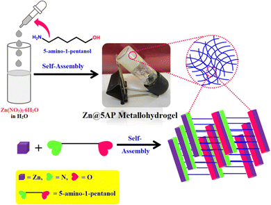
Through the present work, we attempted to establish an eco-friendly method to achieve a rapid self-healable zinc(II) and 5-amino-1-pentanol-based metallohydrogel under ambient reaction conditions at room temperature using water as a solvent (Fig. 1). The available amine and hydroxyl groups in the gelator are responsible for rapid gelation via non-covalent interactions with Zn(II)-ions in the presence of water molecules and the resulting gel network acts as an ideal soft scaffold. Based on the synthesized Zn(II)-metallohydrogel (Zn@5AP) mediated metal–semiconductor (MS) junctions, we have successfully developed non-volatile resistive random access memory (RRAM) devices. Our approach to creating a versatile, useful soft gel scaffold may develop the field of memory devices based on science and technology for applications in neuromorphic computing and data-driven applications like the Internet of Things (IoT), 5G connectivity, etc.
2. Experimental
2.1. Materials
Zinc nitrate hexahydrate (98% reagent grade) and 5-amino-1-pentanol were bought from Sigma-Aldrich chemical company and used as received. The tests were all done using double-distilled water.2.2. Apparatus and measurements
UV-vis absorption spectral data was collected using a SHIMADZU made UV-3101PC model spectrophotometer.The rheological investigation was performed utilizing a 20 mm SS parallel plate geometry and a Peltier plate temperature system set to 25 °C on a DHR-2 stress-controlled rheometer, supplied by TA Instruments.
FESEM pictures were collected by a Carl Zeiss SUPRA 55VP instrument.
TEM images were conducted in an aberration corrected FEI Titan Themis operating at 300 kV.
The ZEISS EVO 18 microscope was used to conduct elemental mapping and EDX tests.
A JASCO FTIR 4700 spectrometer was used to collect the FTIR data.
The current–voltage (I–V) measurements of our synthesized metallohydrogel material-based devices were performed at room temperature using a Keithley 2400 sourcemeter interfaced through Labview.
2.3. Synthesis of the zinc(II)-metallohydrogel
A white colour stable Zn(II)-metallohydrogel (Zn@5AP) was formed during direct mixing of a 500 μL aqueous solution of Zn(NO3)2·6H2O (0.297 g, 1 mM) and 500 μL of pure 5-amino-1-pentanol under ambient conditions (Fig. 1). Fig. 1 shows the synthetic technique and inverted image of the Zn(II)-metallohydrogel and demonstrates the stability of the hydrogel. See Table S1 (ESI†) for the gelation ability procedure of the Zn(II)-metallohydrogel (Zn@5AP) in different solvents.2.4. Determination of minimum critical gelation concentration (MGC) and gel-melting temperature (Tgel)
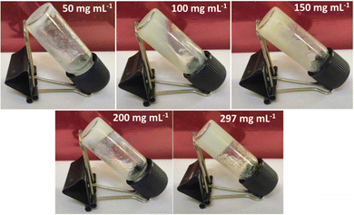
By varying the concentration of Zn(II)-metallohydrogel from 50 mg mL−1 to 297 mg mL−1, it was established that the minimum critical gelation concentration (MGC) of the Zn@5AP metallohydrogel was efficiently formed at a concentration of 256 mg mL−1 (Fig. 2). Zn@5AP has a gel to sol transition temperature (Tgel) of 180 °C.3. Results and discussion
3.1. Rheological analysis
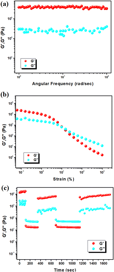
Rheological experiments, such as the storage modulus (G′) and loss modulus (G′′), validated the viscoelastic semi-solid characteristics of the Zn(II)-metallohydrogel (Fig. 3a). When shear is applied to the viscoelastic area, the system stores energy, denoted by the quantity G′ and it is represented as (σ0/γ0) cos(δ), whereas the energy lost due to oscillatory stress is denoted by the symbol G′′ and it is represented as (σ0/γ0) sin(δ). In order for a material to be considered as a gel, the condition G′(ω) > G′′(ω) [where, G′(ω) ≈ ω° and the angular frequency is ω] has to be satisfied. Experimental rheology on a Zn(II)-metallohydrogel at a fixed concentration of Zn(NO3)2·6H2O (i.e. [Zn(II)] = 297 mg mL−1) revealed that the storage modulus (G′) was much higher than the loss modulus (G′′) (i.e. G′ ≫ G′′) (Fig. 3a). As shown by the rheological data, the Zn(II)-metallohydrogel retains its gel structural structure and exhibits solid-like behaviour. Since its average storage modulus (G′) is so much greater than its loss modulus (G′′), the Zn(II)-metallohydrogel has a very high tolerance limit (Fig. 3a). Fig. 3b depicts a strain-sweep experiment performed on the Zn(II)-metallohydrogel material at a constant frequency of 6.27997 rad s−1. Results from the strain-sweep experiment show that the critical strain, the lowest strain for gel breakdown of the Zn(II)-metallohydrogel, occurs at a strain of 0.45%, when G′ mixes with G′′ (Fig. 3b).However, the storage modulus (G′) crosses loss modulus (G′′) when the strain reaches ∼0.1%, demonstrating gel-to-sol transition. Finally, to discern the self-healing behavior, a thixotropy test was performed (Fig. 3c). Interestingly, the soft material remains in the gel state when the strain is ∼0.01%, but it turns into a sol immediately upon sudden increase of the strain to ∼100%. Upon removal of the high strain, the soft material turns into a viscoelastic gel state almost immediately. Such successive low/high strain cycles were repeated, which clearly showed the reversible transition of the soft material from gel-to-sol state, which in turn, demonstrated the self-healing behaviour of the metallohydrogel.
3.2. Self-healing performance of the Zn@5AP metallohydrogel
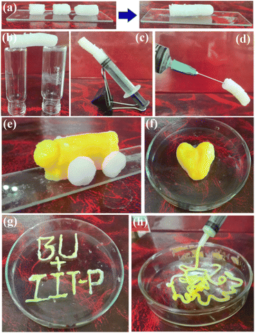
Living organisms exhibit beautiful examples of self-healing properties. The available electronegative N/O-atoms in gelator 5-amino-1-pentanol make the Zn@5AP metallohydrogel a reasonable aspirant to show self-healing properties, as the gelator has a tendency to make good hydrogen bonds with solvent molecules and metal centers.The column of pure Zn@5AP metallohydrogel for testing the self-healing property was prepared following the synthesized method (Fig. 4a). The column was cut into three pieces with dimensions of approximately ∼1–2 cm (Fig. 4a). Block pieces of Zn@5AP were brought back into contact with slight pressure and fully welded to each other in <5 min (Fig. 4a). The cured monolith exhibited a strong edge capable of free standing without any external support (Fig. 4b). The stability of the monoliths after curing against gravity is also revealed in Fig. 4c and d. Furthermore to investigate the molding nature of the Zn@5AP metallohydrogel, it was formed into the shape of a toy car and heart without losing any fluid and maintained its stability without external support, demonstrating its extraordinary moldable properties (Fig. 4e and f). In addition, a sketch was drawn to show the use of the Zn@5AP metallohydrogel as an ink (Fig. 4g). Zn@5AP metallohydrogel was also used to prepare nodule-shaped patterns using a surgical syringe (Fig. 4h), demonstrating that Zn@5AP metallohydrogel can be used for injection.
3.3. Microstructural study
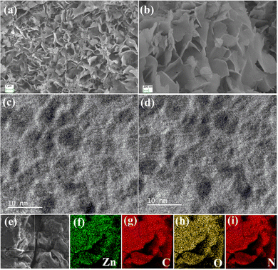
To learn more about the microstructural patterns of the Zn@5AP metallohydrogel, FESEM and TEM structural analysis was accomplished. The FESEM pattern of the Zn@5AP metallohydrogel showed a coriander-leaf like hierarchical network (Fig. 5a and b). The hydrogel's morphology seen under FESEM was generated through the combination of Zn(NO3)2·6H2O and 5-amino-1-pentanol gelator to a water medium and their subsequent rapid mixing.Self-assembly of Zn(II) ions and 5-amino-1-pentanol is the outcome of hydrogelation through various supramolecular interactions like hydrogen bonding patterns, appropriate metal–ligand coordination, electrostatic connections, and hydrophobic interactions. These microstructures were part of the layered structure of the Zn@5AP metallohydrogel and had an average diameter of about ∼1 μm. High resolution TEM images show the hemi-spherical shape of the Zn@5AP metallohydrogel samples (Fig. 5c and d). EDS elemental mapping in Fig. 5e–i confirms the presence of Zn, C, O and N elements of Zn(NO3)2·6H2O, the 5-amino-1-pentanol gelator and the water solvent, accountable in Zn@5AP metallohydrogel networks.
3.4. FT-IR analysis of the Zn@5AP metallohydrogel
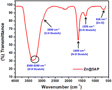
The FT-IR spectral analysis of the Zn@5AP metallohydrogel in its xerogel form reveals the predominant interaction of 5-amino-1-pentanol with the Zn(II)-source in metallohydrogel formation (Fig. 6). The wide broad peaks in the region of 3340–3240 cm−1 are due to O–H stretching vibrations. Vibrational modes at 2950 cm−1 are attributed to C–H stretching vibrations. The vibrational modes associated with the peaks at 1639 cm−1 and 1355 cm−1 are N–O stretching and C–N stretching, respectively. To further prove the strength of association between 5-amino-1-pentanol and an aqueous solution of zinc nitrate, a peak at 618 cm−1 can be observed in the spectrum (Fig. 6), which is due to the presence of Zn–O bonds endorsing the metallohydrogelation.3.5. Optical characterization
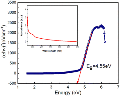
Fig. 7 shows the Tuac's plot to examine the optical properties of the synthesized Zn@5AP based metallogel from UV-vis absorption spectra. The wavelength range was used from 250 nm to 800 nm for the optical measurement (refer to the UV-vis absorption spectra). The optical bandgap (Eg) of the Zn@5AP metallogel was calculated using Tauc's equation, represented by (eqn (1)), using the UV-vis spectrum:| (αhν)n = A(hν − Eg) | (1) |
In electron transition processes, the exponent “n” functions as a dependent constant. “A” refers to a constant with the value 1. Using n = 2, the direct optical band gap was computed. We determined the direct optical band gap (Eg), which is assumed to be 4.55 eV, by expanding the linear region of the plot (αhν)2versus hν (Fig. 7) to α = 0 absorption.
3.6. Device fabrication
In this study, we created a lateral Schottky diode-like structure based on a metal-semiconductor junction in the ITO (indium tin oxide)/Zn@5AP/ITO configuration to perform the electrical studies of the synthesised material (referred to as device 1). We used the Doctor's blade technique to grow a thin film of as-synthesised Zn@5AP metallogel on a glass substrate covered in ITO to build the junction device, and we then annealed the film to remove the solvent. ITO is excellent for studies involving photo-excitations because it is strongly conducting and optically transparent in the visible region of the electromagnetic spectrum.In order to design RRAM (resistive random access memory) devices based on the Zn@5AP metallohydrogel, vertically placed layers in a sandwiched structure of ITO/Zn@5AP/Cu (called device 2) and Cu/Zn@5AP/Cu were prepared (named device 3). The bottom electrodes were cleaned using an ultrasonicator in both designs, which were followed by the deposition of the Zn@5AP metallogel on the substrate and the addition of the top electrode on the samples. The thickness of Zn@5AP is around 200 nm and the dimension of the device is 1 cm × 1 cm. The device structures are given in Table 1.
| Device no. | Device structure | Dimensions of the device |
|---|---|---|
| Device 1 | ITO/Zn@5AP/ITO | 1 cm × 1 cm |
| Device 2 | ITO/Zn@5AP/Cu | 1 cm × 1 cm |
| Device 3 | Cu/Zn@5AP/Cu | 1 cm × 1 cm |
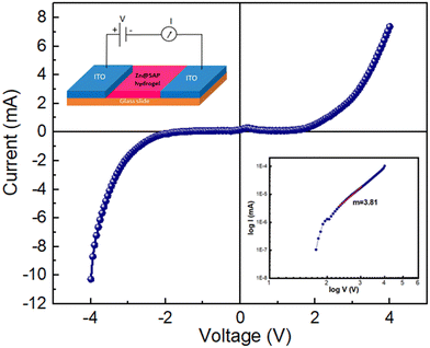
In order to get a detailed understanding of the semiconducting nature of the Zn@5AP metallohydrogel in the thin film geometry, its charge transport properties were measured in a two-probe configuration. There is no discernible conduction in the voltage region (−5 V to +5 V), where the I–V curve of device 1 is shown in Fig. 8 on a linear scale. The current was found to increase rapidly with an increase in voltage in both the positive and negative polarities. The main diode parameters were then extracted from the non-linear Schottky diode's I–V curve using the thermionic emission theory (TE Theory) after analysing the I–V data as suggested by Cheung.47 We note that the semiconductor with SBs at both contacts can be modeled with two back-to-back Schottky diodes separated by a series resistance. When a sufficiently high external voltage is applied, whether a positive or negative, one Schottky junction is forward-biased while the other one is reverse-biased. The reverse saturation current of the reverse-biased diode always limits the current.
Based on thermionic emission, the current at the two contacts can be written as,
 | (2) |
 | (3) |
 | (4) |
 | (5) |
 | (6) |
 can be expressed as
 | (7) |
 | (8) |
 | (9) |
 ,We obtain,
 | (10) |
 | (11) |
 can be neglected in the denominator of eqn (10), that reduces to the single SB equation.
 | (12) |
![[thin space (1/6-em)]](https://www.rsc.org/images/entities/char_2009.gif) I vs. log
I vs. log![[thin space (1/6-em)]](https://www.rsc.org/images/entities/char_2009.gif) V graph, which is shown in Fig. 8 (right: inset), in order to completely comprehend the conduction mechanism. The current flow is governed by the space charge conduction mechanism in the higher voltage region with a slope of 3.81.
V graph, which is shown in Fig. 8 (right: inset), in order to completely comprehend the conduction mechanism. The current flow is governed by the space charge conduction mechanism in the higher voltage region with a slope of 3.81. | (13) |
 | (14) |
| H(I) = IRS + ηϕB | (15) |
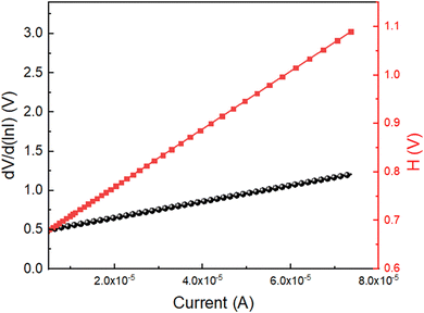
The series resistance, ideality factor, and barrier potential height were calculated using eqn (13)–(15). These formulas were produced by simply deriving from Cheung's theory. We plotted the dV/d(ln![[thin space (1/6-em)]](https://www.rsc.org/images/entities/char_2009.gif) I) vs. I graph and H vs. I graph, as shown in Fig. 9, in order to determine the diode parameters of device 1. We determined the barrier height from the intercept of the H vs. I graph and the ideality factor (η) from the intercept of the dV/d(ln
I) vs. I graph and H vs. I graph, as shown in Fig. 9, in order to determine the diode parameters of device 1. We determined the barrier height from the intercept of the H vs. I graph and the ideality factor (η) from the intercept of the dV/d(ln![[thin space (1/6-em)]](https://www.rsc.org/images/entities/char_2009.gif) I) vs. I graph. The ideality factor (η) for our diodes was determined to be 25.13, which is greater than the ideal value of 1.1. The series resistance at the interface, the presence of interface states, and the presence of inhomogeneities in the Schottky barrier55 could all contribute to the divergence of the expected behaviour.
I) vs. I graph. The ideality factor (η) for our diodes was determined to be 25.13, which is greater than the ideal value of 1.1. The series resistance at the interface, the presence of interface states, and the presence of inhomogeneities in the Schottky barrier55 could all contribute to the divergence of the expected behaviour.
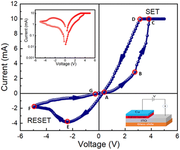
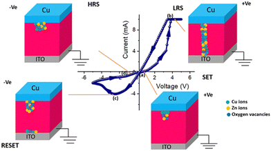
A barrier height (ϕB) of 0.03 eV was determined for device 1. The fabricated diode structure clearly has a lower barrier potential height and a greater ideality factor and these two characteristics are essential for designing a Schottky diode. We computed the slope of the dV/d(ln![[thin space (1/6-em)]](https://www.rsc.org/images/entities/char_2009.gif) I) vs. I graph as well as the H vs. I graph in order to obtain the value of the series resistance, which is 5963.04 Ω. After taking into consideration all of the measured properties, it can be stated that such diode layouts can be useful for semiconductor electronics design. We have also measured I–V characteristics at different low temperatures from 100 K to 200 K, as shown in Fig. S4 (ESI†). I–V measurements are also used to examine the resistive switching behaviour of the Zn@5AP metallohydrogel-based heterostructure (see Fig. 10 (right: inset)) where ITO acts as the bottom electrode and Cu acts as the top electrode in device 2. To avoid any leakage contribution to the I–V measurements, the compliance current (CC) is set at 100 mA before the commencement of any tests. The I–V trajectory of device 2 is displayed on a linear scale in Fig. 10. In this instance, the I–V measurements are performed in the following sequence: 0 V → 5 V → −5 V → 0 V. The applied voltage is shown by the arrows. The I–V loop displays complete hysteresis, which is an indication of memristive behaviour. The current across the low-voltage zone initially rises linearly when the voltage is close to 0 V (point A to point B). Non-linearity in the current–voltage graph is seen under a specific voltage (2.829 V), and as the applied voltage increases, the current increases abruptly. The device is now transitioning from a higher resistance state (HRS) to a lower resistance state (LRS), according to the SET voltage (VSET = 2.829 V). At point C, the current increases. Then, even if the voltage is switched from point C to point D, the device maintains its ON state. After the voltage drops, the current starts to rapidly decrease at point E, and the device turns into the OFF state. After cycling in the opposite direction, the current keeps increasing and achieves an LRS at a value of −2.43 V (point E).
I) vs. I graph as well as the H vs. I graph in order to obtain the value of the series resistance, which is 5963.04 Ω. After taking into consideration all of the measured properties, it can be stated that such diode layouts can be useful for semiconductor electronics design. We have also measured I–V characteristics at different low temperatures from 100 K to 200 K, as shown in Fig. S4 (ESI†). I–V measurements are also used to examine the resistive switching behaviour of the Zn@5AP metallohydrogel-based heterostructure (see Fig. 10 (right: inset)) where ITO acts as the bottom electrode and Cu acts as the top electrode in device 2. To avoid any leakage contribution to the I–V measurements, the compliance current (CC) is set at 100 mA before the commencement of any tests. The I–V trajectory of device 2 is displayed on a linear scale in Fig. 10. In this instance, the I–V measurements are performed in the following sequence: 0 V → 5 V → −5 V → 0 V. The applied voltage is shown by the arrows. The I–V loop displays complete hysteresis, which is an indication of memristive behaviour. The current across the low-voltage zone initially rises linearly when the voltage is close to 0 V (point A to point B). Non-linearity in the current–voltage graph is seen under a specific voltage (2.829 V), and as the applied voltage increases, the current increases abruptly. The device is now transitioning from a higher resistance state (HRS) to a lower resistance state (LRS), according to the SET voltage (VSET = 2.829 V). At point C, the current increases. Then, even if the voltage is switched from point C to point D, the device maintains its ON state. After the voltage drops, the current starts to rapidly decrease at point E, and the device turns into the OFF state. After cycling in the opposite direction, the current keeps increasing and achieves an LRS at a value of −2.43 V (point E).
At a RESET voltage (VRESET) of −4.8 V, the device returns to the HRS. The system changes from LRS to HRS using the RESET method, which is denoted by the arrow between points F and G. This is a crucial indicator of the sample's bipolar resistive switching behaviour because a negative voltage is required to return the sample to its prior resistance state. The I–V properties of device 2 are displayed on a semi-logarithmic scale in Fig. 10 (left: inset). The increase and decrease in current caused by the formation and rupture of conductive filament-type structures tries to switch the device between the ON and OFF states. We have also measured the complete I–V curves of device 2 for consecutive cycles and observed some variability in the first few cycles (∼20) as shown in Fig. S1 (ESI†) which gets stabilized. Later, this mechanism is described.
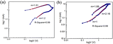
In order to better understand the conduction mechanism and the charge transport mechanism of device 2, we have fitted the I–V curve in the logarithmic scale (Fig. 11a) throughout the SET process. In this instance, we have come to the conclusion that the current exhibits ohmic conduction and changes linearly in the voltage range of 0 V to 3 V with a slope of m = 1. But in the higher voltage region, the current follows space charge limited conduction behaviour with a slope of m = 2.16. It is confirmed that it is followed by space charge conduction behaviour when the slope is around 2. Similar behaviour has also been exposed by the RESET process (Fig. 11b). We have noticed that it exhibits ohmic behaviour with a slope of m = 1.2 in the lower voltage region between 0 V and 3 V.
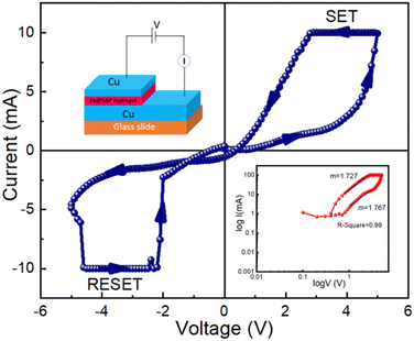
In order to observe the resistive switching characteristics of device 3, Cu is used as both the top and bottom electrodes in device 3. In the presence of the SET and RESET operations (VSET = 4.98 V and VRESET = −4.58 V), the I–V curve exhibits memristive behaviour over full voltage cycling with discrete LRS and HRS states, as shown in Fig. 12. This behaviour resembles the I–V curve of device 2 in the same way. We have also measured the complete I–V curves of device 3 for consecutive cycles and observed some variability in the first few cycles (∼20) as shown in Fig. S2 (ESI†) which gets stabilized later. For comparing device 3 with device 2, we have observed that there is some variation in the I–V curve in the complete cyclic response, which is shown in Fig. S3 (ESI†).
For a better understanding of the conduction mechanism and the charge transport process of device 3, we have also fitted the I–V curve in the logarithmic scale in the SET process (Fig. 12 (right: inset)). We have observed that the current follows the ohmic nature of conduction and varies linearly with a slope of m = 1.76.
We also plotted the I–V curve using a logarithmic scale during the RESET procedure (Fig. 13). Here, we have seen that it exhibits ohmic behaviour with a slope of 1.13 in the voltage range between 0 V and 4 V.
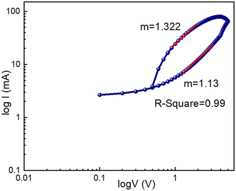 | ||
| Fig. 13 I–V curve of the glass/Cu/Zn@5AP/Cu based device on a logarithmic scale in the RESET process. | ||
To better understand the consistency of the switching process, we also performed an endurance test for 5000 switching cycles consecutively at room temperature for both the devices (2 and 3), as shown in Fig. 14(a) and (b). The switching procedure for device 2 and 3 is reliable for up to 5000 switching cycles. The endurance test shows that the switching behaviour is robust because the average ON/OFF ratio is around 100 for both the devices. This implies that this device can continue to function as intended in terms of memory response over an extended period without experiencing any degradation, which is helpful for real-world uses in memory circuit design at a reduced cost of production.
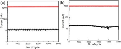 | ||
| Fig. 14 (a) Endurance test of the glass/ITO/Zn@5AP/Cu based device; (b) endurance test of the glass/Cu/Zn@5AP/Cu based device. | ||
We have also performed retention tests for up to 1000 s at room temperature for both the devices (2 and 3), as shown in Fig. 15(a) and (b). The switching procedure for devices 2 and 3 is reliable for up to 103 s. We have also observed that for both the devices (2 and 3) the ON/OFF ratio is around 85. From the retention test, we can conclude that these devices can store data up to 103 s without any degradation.
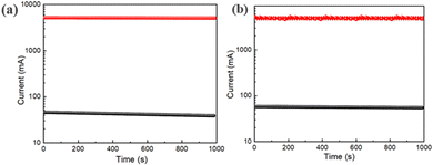 | ||
| Fig. 15 (a) Retention test of the glass/ITO/Zn@5AP/Cu based device; (b) retention test of the glass/Cu/Zn@5AP/Cu based device. | ||
A comparison of ION/IOFF observed in other materials at room temperature (shown in Table 2).
Numerous processes, such as the formation of the Schottky barrier with electrochemical migration, redox reactions, valence change memory, etc. can be used to explain the physical origin of the switching process. According to our study, the valence change memory (VCM) and electrochemical metallization (ECM) process are impacted by the mobility of oxygen defects and metal cations. Here, it is shown that metal ions and oxygen vacancies both have a substantial impact on the change in resistance (Fig. 16). For device 2, conducting filaments form in the semiconducting layers and as a result there is the migration of Cu ions, Zn ions, and oxygen vacancies. We can explain the transition from the HRS to LRS state by rupturing and regenerating the Cu filaments that are integrated into the semiconducting layers. In this study, the resistive switching behaviour of device 2 is mainly caused by the migration of Cu ions and oxygen vacancies. We already know that copper ions can move in the direction of an applied electric field and ionize in the presence of an electric field to generate copper ions with the formula Cu → Cu2+ + e−. When a positive voltage is applied, Cu2+ ions, Zn ions, and oxygen vacancies travel towards the intermediate layer where they are transformed into metallic Cu. After the SET process is complete and the device switches from HRS to LRS, the conductivity of this layer will rise and the concentration of Cu ions, Zn ions, and oxygen vacancies will approach the bottom electrode. Until a sufficient voltage with the opposite polarity is applied to electrochemically dissolve the Cu filaments and oxygen vacancies for the RESET operation, the device stays in the LRS state. The device enters the HRS when negative voltage is applied, and its conductivity also drops at the same moment. At the end, Cu2+, Zn, and oxygen vacancy ions return to the upper electrode. In this way, the resistive switching behaviour of device 3 can be described by the migration of Cu2+ ions, Zn ions, and oxygen vacancies. We have also described the conduction filament model from TEM and EDAX analysis, as shown in Fig. S5 (ESI†) (Table 3).
| RRAM device | Endurance (cycles) | Retention (s) | ON/OFF ratio | Power consumption (nW) | Ref. |
|---|---|---|---|---|---|
| Al2O3/ZnO-based RRAM | 104 | 104 | 105 | 1.4 × 10⁴ | 56 |
| Pt/AlOx/ZnO/Ti | 103 | 104 | 102 | 0.6 | 57 |
| Pt/HfO2/TiOx/Pt | 100 | 104 | 102 | 1.12 × 10³ | 58 |
| Graphene/HfO2/TiN | 103 | 104 | 102 | 4.6 × 10² | 59 |
| hhBN/AlOx/TiOx/Ito | 100 | 104 | 102 | 2 × 10³ | 60 |
| Cu/Zn@5AP/ITO | 5000 | 103 | 102 | 4.72 × 10³ | This work |
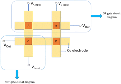
Memory devices in memory systems are organized in arrays, and one common architecture is the cross-point architecture. In this configuration, our sample is placed at the crossing point of two perpendicular metal lines, as shown in Fig. 17. In our research work, we have shown how the metallogel-based RRAM device in a crossbar array works in memory computing using logic gate operation. In-memory computing can also be accomplished by employing fundamental electrical circuit principles, such as Kirchhoff's law and Ohm's law. This method is particularly well-suited for analog crossbar arrays. Here, in this work we have prepared a 2 × 2 cross bar device based on a Cu/Zn@5AP/Cu structure where Cu acts as both the top and bottom electrode as shown in Fig. 17 and the four RRAM devices are denoted by A, B, C, and D.
Now, for logic gate operations we have used two RRAM devices (A and B). For the OR logic gate, if memristors A and B are both logical “0” that means no voltage is applied, and then the output voltage is 0.143 V which is considered as the “0” state. When we applied 5 V at input A and 0 V at input B, then the output voltage is 4.96 V which is considered as the logical “1” state. Similarly, when we applied 0 V at input A and 5 V at input B, then the output voltage is 4.95 V which is also considered as the logical “1” state. When both memristors A and B are both in the logical “1” state, that means when we applied 5 V at both the terminals, then the output voltage is also 4.95 V as the logical “1” state. The truth table of the OR logic gate is shown in Table 4.
| Voltage at input A (V) | Voltage at input B (V) | Output voltage (V) | Logical state |
|---|---|---|---|
| 0 | 0 | 0.14 | 0 |
| 5 | 0 | 4.96 | 1 |
| 0 | 5 | 4.95 | 1 |
| 5 | 5 | 4.95 | 1 |
Similarly, we have designed a NOT gate logic circuit (shown in Fig. 17) using device C and it also satisfied a NOT gate truth table, which is shown in Table 5.
| Input voltage | Output voltage | Logical state |
|---|---|---|
| 0 V | V | 1 |
| 5 V | 0.11 V | 0 |
The current structure can be extended further with a larger size of cross-point arrays to perform advanced logic and computing operations, which can act as a central part for in-memory computing where the computation and information storage are done at the same circuit level, as demonstrated here. In this way, memristor based logic gate circuits using crossbar arrays will help us to explore different engineering methodologies that depend on in-memory computing principles.
4. Conclusions
In conclusion, a novel supramolecular Zn(II)-metallohydrogel was synthesized by one-shot mixing of an aqueous solution of Zn(II)-ions and 5-amino-1-pentanol low molecular weight gelator. The mechanical strength and self-healing properties of the synthesized hydrogel were established through rheological investigations and thixotropic study. The hierarchical morphological features of the Zn(II)-metallohydrogel were shown through FESEM and TEM images. The primary strategy of gel formation via different potential intermolecular interactions was recognized through FT-IR spectroscopic study. In this work we have prepared ITO/Zn@5AP/Cu and Cu/Zn@5AP/Cu based RRAM devices and the bipolar resistive switching behaviour is investigated of these devices. The resistive switching behaviour of these two heterostructures is caused by the formation and rupture of conduction filaments between the vertical electrodes. This RRAM device shows an excellent ON/OFF ratio, which is around 100 across 5000 switching cycles without any degradation in performance. Because of its strong resistive switching behaviour, exceptional endurance, and high ON/OFF ratio, the Zn(II)-metallohydrogel is a promising material for non-volatile memory applications. Therefore, the Zn(II)-metallohydrogel is preferable for applications in neural network circuit design, and neuromorphic and in-memory computing.Conflicts of interest
The authors declare no competing financial interests.Acknowledgements
S. D. expresses gratitude to the UGC, New Delhi, for the conferred Dr DS Kothari Postdoctoral Fellowship (award letter number no. F.4-2/2006 (BSR)/CH/19-20/0224). S. B. appreciates the support from DST Inspire Faculty Research Grant (Faculty Registration No. IFA18-CH304; DST/INSPIRE/04/2018/000329).Notes and references
- J. W. Steed, Supramolecular gel chemistry: developments over the last decade, Chem. Commun., 2011, 47, 1379–1383 RSC.
- M.-O. M. Piepenbrock, G. O. Lloyd, N. Clarke and J. W. Steed, Metal- and Anion-Binding Supramolecular Gels, Chem. Rev., 2010, 110, 1960–2004 CrossRef CAS PubMed.
- S. Dhibar, A. Dey, A. Dey, S. Majumdar, D. Ghosh, P. P. Ray and B. Dey, Development of Supramolecular Semiconducting Mn(ii)-Metallogel Based Active Device with Substantial Carrier Diffusion Length, ACS Appl. Electron. Mater., 2019, 1, 1899–1908 CrossRef CAS.
- P. Dastidar, Supramolecular gelling agents: can they be designed?, Chem. Soc. Rev., 2008, 37, 2699–2715 RSC.
- A. R. Hirst, B. Escuder, J. F. Miravet and D. K. Smith, High-tech applications of self-assembling supramolecular nanostructured gel-phase materials: from regenerative medicine to electronic devices, Angew. Chem., Int. Ed., 2008, 47, 8002–8018 CrossRef CAS PubMed.
- J. A. Foster, M.-O. M. Piepenbrock, G. O. Lloyd, N. Clarke, J. A. K. Howard and J. W. Steed, Anion-switchable supramolecular gels for controlling pharmaceutical crystal growth, Nat. Chem., 2010, 2, 1037–1043 CrossRef CAS PubMed.
- N. M. Sangeetha and U. Maitra, Supramolecular gels: Functions and uses, Chem. Soc. Rev., 2005, 34, 821–836 RSC.
- Z. Yang, G. Liang and B. Xu, Enzymatic hydrogelation of small molecules, Acc. Chem. Res., 2008, 41, 315–326 CrossRef CAS PubMed.
- K. Y. Lee and D. J. Mooney, Hydrogels for tissue engineering, Chem. Rev., 2001, 101, 1869–1879 CrossRef CAS PubMed.
- E. Krieg, E. Shirman, H. Weissman, E. Shimoni, S. G. Wolf, I. Pinkas and B. Rybtchinski, Supramolecular Gel Based on a Perylene Diimide Dye: Multiple Stimuli Responsiveness, Robustness, and Photofunction, J. Am. Chem. Soc., 2009, 131, 14365–14373 CrossRef CAS PubMed.
- (a) S. Dhibar, A. Dey, D. Ghosh, S. Majumdar, A. Dey, P. P. Ray and B. Dey, Triethylenetetramine-Based Semiconducting Fe(III) Metallogel: Effective Catalyst for Aryl−S Coupling, ACS Omega, 2020, 5, 2680–2689 CrossRef CAS PubMed; (b) S. Dhibar, A. Dey, R. Jana, A. Chatterjee, G. K. Das, P. P. Ray and B. Dey, A semiconducting supramolecular Co(II)-metallohydrogel: an efficient catalyst for single-pot aryl–S bond formation at room temperature, Dalton Trans., 2019, 48, 17388–17394 RSC.
- L. A. Estroff and A. D. Hamilton, Water Gelation by Small Organic Molecules, Chem. Rev., 2004, 104, 1201–1218 CrossRef CAS PubMed.
- D. Swern, G. N. Billen, T. W. Findley and J. T. Scanlan, Hydroxylation of Monounsaturated Fatty Materials with Hydrogen Peroxide, J. Am. Chem. Soc., 1945, 67, 1786–1789 CrossRef CAS.
- H. Svobodová, V. Noponen, E. Kolehmainen and E. Sievänen, Recent advances in steroidal supramolecular gels, RSC Adv., 2012, 2, 4985–5007 RSC.
- K. Hanabusa, K. Hiratsuka, M. Kimura and H. Shirai, Easy Preparation and Useful Character of Organogel Electrolytes Based on Low Molecular Weight Gelator, Chem. Mater., 1999, 11, 649–655 CrossRef CAS.
- B. Alies, M. A. Ouelhazi, A. N. Patwa, J. Verget, L. Navailles, V. Desvergnes and P. Barthelemy, Cytidine- and guanosine-based nucleotide–lipids, Org. Biomol. Chem., 2018, 16, 4888–4894 RSC.
- C. Tomasini and N. Castellucci, Peptides and peptidomimetics that behave as low molecular weight gelators, Chem. Soc. Rev., 2013, 42, 156–172 RSC.
- R. Rajkamal, N. P. Pathak, D. Chatterjee, A. Paul and S. Yadav, Arabinose based gelators: rheological characterization of the gels and phase selective organogelation of crude-oil, RSC Adv., 2016, 6, 92225–92234 RSC.
- U. S. K. Madduma-Bandarage and S. V. Madihally, Synthetic hydrogels: Synthesis, novel trends, and applications, J. Appl. Polym. Sci., 2021, 138, 50376 CrossRef CAS.
- S. Dhibar, A. Dey, A. Dalal, S. Bhattacharjee, R. Sahu, R. Sahoo, A. Mondal, S. M. Rahaman, S. Kundu and B. Saha, An organic acid consisted multiresponsive self-healing supramolecular Cu(II)-metallogel: Fabrication and analysis of semiconducting device, J. Mol. Liq., 2023, 370, 121021 CrossRef CAS.
- G. Yu, X. Yan, C. Han and F. Huang, Characterization of supramolecular gels, Chem. Soc. Rev., 2013, 42, 6697–6722 RSC.
- R. Roy, M. Bhagyalalitha, P. Choudhury and P. Dastidar, Salt metathesis for developing injectable supramolecular metallohydrogelators as a multi-drug-self-delivery system, Chem. Commun., 2016, 52, 13811–13814 RSC.
- J. Li, L. Geng, G. Wang, H. Chu and H. Wei, Self-Healable Gels for Use in Wearable Devices, Chem. Mater., 2017, 29, 8932–8952 CrossRef CAS.
- N. Malviya, C. Sonkar, R. Ganguly and S. Mukhopadhyay, Cobalt Metallogel Interface for Selectively Sensing L-Tryptophan among Essential Amino Acids, Inorg. Chem., 2019, 58, 7324–7334 CrossRef CAS PubMed.
- J. Puigmartí-Luis, V. Laukhin, Á. Pérezdel Pino, J. Vidal-Gancedo, C. Rovira, E. Laukhina and D. B. Amabilino, Supramolecular conducting nanowires from organogels, Angew. Chem., Int. Ed., 2006, 46, 238–241 CrossRef PubMed.
- S. Dhibar, A. Dey, A. Dey, S. Majumdar, A. Mandal, P. P. Ray and B. Dey, The development of a rapid self-healing semiconducting monoethanolamine-based Mg(OH)2 metallogel for a Schottky diode application with a high ON/OFF ratio, New J. Chem., 2019, 43, 15691–15699 RSC.
- N. Alama and D. Sarma, A Thixotropic Supramolecular Metallogel with 2D Sheet Morphology: Iodine Sequestration and Column Based Dye Separation, Soft Matter, 2020, 16, 10620–10627 RSC.
- S. Majumdar, T. Singha, S. Dhibar, A. Mandal, P. K. Datta and B. Dey, Protein-Based Self-Healing Cu(II)-Metallohydrogels: Efficient ThirdOrder Nonlinear Optical Materials in Terms of an IntensityDependent Refractive Index and Two-Photon Absorption, ACS Appl. Electron. Mater., 2020, 2, 3678–3685 CrossRef CAS.
- S. Majumdar, A. Dey, R. Sahu, S. Dhibar, P. P. Ray and B. Dey, Cd-Based Metallohydrogel Composites with Graphene Oxide, MoS2, MoSe2, and WS2 for Semiconducting Schottky Barrier Diodes, ACS Appl. Nano Mater., 2020, 3, 11025–11036 CrossRef CAS.
- Z. Wei, J. H. Yang, Z. Q. Liu, F. Xu, J. X. Zhou, M. Zrínyi, Y. Osada and Y. M. Chen, Novel Biocompatible Polysaccharide-Based Self-Healing Hydrogel, Adv. Funct. Mater., 2015, 25, 1352–1359 CrossRef CAS.
- (a) A. S. Hoffman, Hydrogels for biomedical applications, Adv. Drug Delivery Rev., 2012, 64, 18–23 CrossRef; (b) F. Xu, C. A. M. Wu, V. Rengarajan, T. D. Finley, H. O. Keles, Y. Sung, B. Li, U. A. Gurkan and U. Demirci, Three-Dimensional Magnetic Assembly of Microscale Hydrogels, Adv. Mater., 2011, 23, 4254–4260 CrossRef CAS PubMed.
- P. G. de Gennes, Reptation of a Polymer Chain in the Presence of Fixed Obstacles, J. Chem. Phys., 1971, 55, 572–579 CrossRef.
- N. Holten-Andersen, M. J. Harrington, H. Birkedal, B. P. Lee, P. B. Messersmith, K. Y. C. Lee and J. H. Waite, pH-induced metal-ligand cross-links inspired by mussel yield self-healing polymer networks with near-covalent elastic moduli, Proc. Natl. Acad. Sci. U. S. A., 2011, 108, 2651–2655 CrossRef CAS PubMed.
- (a) L. Yu and J. Ding, Injectable hydrogels as unique biomedical materials, Chem. Soc. Rev., 2008, 37, 1473–1481 RSC; (b) N. Annabi, A. Tamayol, J. A. Uquillas, M. Akbari, L. E. Bertassoni, C. Cha, C. Gamci-Unal, M. R. Dokmeci, N. A. Peppas and A. Khademhosseini, 25th Anniversary Article: Rational Design and Applications of Hydrogels in Regenerative Medicine, Adv. Mater., 2014, 26, 85–123 CrossRef CAS PubMed.
- J. H. Jung, G. John, M. Masuda, K. Yoshida, S. Shinkai and T. Shimizu, Self-Assembly of a Sugar-Based Gelator in Water:
![[thin space (1/6-em)]](https://www.rsc.org/images/entities/char_2009.gif) Its Remarkable Diversity in Gelation Ability and Aggregate Structure, Langmuir, 2001, 17, 7229–7232 CrossRef CAS.
Its Remarkable Diversity in Gelation Ability and Aggregate Structure, Langmuir, 2001, 17, 7229–7232 CrossRef CAS. - Y. Lee, W. J. Song and J.-Y. Sun, Hydrogel soft robotics, Mater. Today Phys., 2020, 15, 100258 CrossRef.
- M. Caprioli, I. Roppolo, A. Chiappone, L. Larush, C. F. Pirri and S. Magdassi, 3D-printed self-healing hydrogels via Digital Light Processing, Nat. Commun., 2021, 12, 2462–2470 CrossRef CAS PubMed.
- B. Zhang, S. Li, H. Hingorani, A. Serjouei, L. Larush, A. A. Pawar, W. H. Goh, A. H. Sakhaei, M. Hashimoto, K. Kowsari, S. Magdassi and Q. Ge, Highly stretchable hydrogels for UV curing based high-resolution multimaterial 3D printing, J. Mater. Chem. B, 2018, 6, 3246–3253 RSC.
- C. K. Karan and M. Bhattacharjee, Self-Healing and Moldable Metallogels as the Recyclable Materials for Selective Dye Adsorption and Separation, ACS Appl. Mater. Interfaces, 2016, 8, 5526–5535 CrossRef CAS PubMed.
- S. Dey, D. Datta, K. Chakraborty, S. Nandi, A. Anoop and T. Pathak, A coordination-assisted general approach to nickel-based nano metallogels, RSC Adv., 2013, 3, 9163–9166 RSC.
- K. Karuna, A. Kumar, D. K. Kotnees, J. Balakrishnan, A. D. Thakur and S. J. Ray, Structural and resistive switching behaviour in lanthanum strontium manganite-Reduced graphene oxide nanocomposite system, J. Alloys Compd., 2020, 815, 152213 CrossRef.
- K. Kumari, A. Kumar, A. D. Thakur and S. J. Ray, Charge transport and resistive switching in a 2D hybrid interface, Mater. Res. Bull., 2021, 139, 111195 CrossRef CAS.
- K. Karuna, S. Majumder, A. D. Thakur and S. J. Ray, Temperature-dependent resistive switching behaviour of an oxide memristor, Mater. Lett., 2021, 303, 130451 CrossRef.
- K. Kumari, A. D. Thakur and S. J. Ray, The effect of graphene and reduced graphene oxide on the resistive switching behavior of La0.7Ba0.3MnO3, Mater. Today Commun., 2021, 26, 102040 CrossRef CAS.
- K. Kumari, S. Kar, A. D. Thakur and S. J. Ray, Role of an oxide interface in a resistive switch, Curr. Appl. Phys., 2022, 35, 16–23 CrossRef.
- N. Alam, S. Majumder, S. J. Ray and D. Sarma, A wide bandgap semiconducting magnesium hydrogel: moisture harvest, iodine sequestration, and resistive switching, Langmuir, 2022, 38, 10601–10610 CrossRef CAS PubMed.
- S. K. Cheung and N. W. Cheung, Extraction of Schottky diode parameters from forward current-voltage characteristics, Appl. Phys. Lett., 1986, 49, 85–87 CrossRef CAS.
- S. Majumder, K. Kumari and S. J. Ray, Temperature-dependent resistive switching behavior of a hybrid semiconductor-oxide planar system, Appl. Phys. A: Mater. Sci. Process., 2023, 129, 1–10 CrossRef.
- A. Kumar, K. Kumari, S. J. Ray and A. D. Thakur, Graphene mediated resistive switching and thermoelectric behavior in lanthanum cobaltate, J. Appl. Phys., 2020, 127, 235103 CrossRef CAS.
- K. Karmakar, A. Roy, S. Dhibar, S. Majumder, S. Bhattacharjee, B. Mondal, S. K. M. Rahaman, R. Saha, S. J. Ray and B. Saha, Instantaneous Gelation of a Self-Healable Wide-Bandgap Semiconducting Supramolecular Mg(II)-Metallohydrogel: An Efficient Nonvolatile Memory Design with Supreme Endurance, ACS Appl. Electron. Mater., 2023, 5, 3340–3349 CrossRef CAS.
- B. Sun, X. Zhang, G. Zhou, P. Li, Y. Zhang, H. Wang, Y. Xia and Y. Zhao, An organic nonvolatile resistive switching memory device fabricated with natural pectin from fruit peel, Org. Electron., 2017, 42, 181–186 CrossRef CAS.
- K. Kumari, A. D. Thakur and S. J. Ray, Structural, resistive switching and charge transport behaviour of (1 − x)La0.7Sr0.3MnO3·(x)ZnO composite system, Appl. Phys. A: Mater. Sci. Process., 2022, 128, 992 CrossRef CAS.
- K. Kumari, S. J. Ray and A. D. Thakur, Resistive switching phenomena: a probe for the tracing of secondary phase in manganite, Appl. Phys. A: Mater. Sci. Process., 2022, 128, 430 CrossRef CAS.
- S. Majumder, K. Kumari and S. J. Ray, Pulsed voltage induced resistive switching behavior of copper iodide and La0.7Sr0.3MnO3 nanocomposites, Mater. Lett., 2021, 302, 130339 CrossRef CAS.
- A. Grillo and A. D. Bartolomeo, A Current–Voltage Model for Double Schottky Barrier Devices, Adv. Electron. Mater., 2021, 7, 2000979 CrossRef CAS.
- J. W. Seo, J.-W. Park, K. S. Lim, S. J. Kang, Y. H. Hong, J. H. Yang, L. Fang, G. Y. Sung and H.-K. Kim, Transparent flexible resistive random access memory fabricated at room temperature, Appl. Phys. Lett., 2021, 95, 133508 Search PubMed.
- M.-C. Wu, J.-Y. Chen, Y.-H. Ting, C.-Y. Huang and W.-W. Wu, A novel high-performance and energy-efficient RRAM device with multi-functional conducting nanofilaments, Nano Energy, 2021, 82, 105717 CrossRef CAS.
- X. Ding, Y. Feng, P. Huang, L. Liu and J. Kang, Low-power resistive switching characteristic in HfO2/TiOx bi-layer resistive random-access memory, Nanoscale Res. Lett., 2019, 14, 157 CrossRef PubMed.
- S. Lee, J. Sohn, Z. Jiang, H.-Y. Chen and H. S. Philip Wong, Metal oxide-resistive memory using graphene-edge electrodes, Nat. Commun., 2015, 6, 8407 CrossRef PubMed.
- Y.-J. Huang and S.-C. Lee, Graphene/h-BN heterostructures for vertical architecture of RRAM design, Sci. Rep., 2017, 7, 9679 CrossRef PubMed.
Footnotes |
| † Electronic supplementary information (ESI) available. See DOI: https://doi.org/10.1039/d3ma00765k |
| ‡ AR and SD should be treated as joint first authors |
| This journal is © The Royal Society of Chemistry 2024 |

