 Open Access Article
Switching from binary to ternary WORM memory behavior of benzothiadiazole-based D–A system†
Paliyottil Kesavan
Bhagyanath
a,
Varghese Maria
Angela
a,
Hait
Asit
a,
Predhanekar M.
Imran
b,
Nattamai S. P.
Bhuvanesh
c and
Samuthira
Nagarajan
 *a
*a
aDivision of Organic Electronics, Department of Chemistry, Central University of Tamil Nadu, Thiruvarur-610 005, India. E-mail: snagarajan@cutn.ac.in
bDepartment of Chemistry, Islamiah College, Vaniyambadi – 635 752, India
cDepartment of Chemistry, Texas A&M University, College Station, TX 77842, USA
First published on 1st March 2024
Abstract
A series of novel benzothiadiazole (BTD) derivatives was synthesized via a Pd-catalyzed Suzuki-cross-coupling reaction, encompassing compounds with D–A–D and D–A–A architectures. Devices featuring non-symmetrical structures incorporating electron-accepting cyano and nitro groups on the BTD core exhibited a non-volatile ternary WORM memory behavior. Conversely, symmetrical compounds containing di-tertiary-butyl or dimethoxy groups as donors manifested binary memory behavior. The compounds with methoxyl and cyano substitution in the D–A–A architecture displayed only binary switching behavior due to their unfavorable thin film formation and molecular packing. UV and CV data analysis revealed narrow band gaps ranging from 2.58 to 2.75 eV, facilitating charge carrier transport within the active layer. Remarkably, compounds featuring t-Bu and cyano group substitutions showcased superior performance attributes, characterized by a low threshold voltage of −0.80 V and a high ON/OFF ratio of 102. The underlying resistive switching mechanism was elucidated through analysis of HOMO, LUMO, and ESP studies, indicating a composite influence of charge transfer and charge trapping phenomena. This study highlights the significant influence of substituent modifications in D–A molecules on molecular packing, thin film morphology, and electron trap depth within the active layer. These factors profoundly impact the memory performance of organic memory devices.
Introduction
The miniaturization of silicon-based transistors is challenging due to the physical limits and quantum tunneling phenomena of electrons.1 This will limit the future creation of smaller, faster, more powerful transistors, and as a result, the world is shifting to organic memory devices. In contrast to conventional silicon-based memory architectures, which rely on encoding “0” and “1” based on the quantity of stored charge, organic molecules offer a distinctive approach to charge storage predicated upon electrical bistability. This bistability encompasses discrete high and low resistive states (HRS/LRS). The transition from an HRS to a LRS analogously mirrors the binary conversion from ‘0’ to ‘1’. Additionally, multiple bistable states such as HRS, LRS1, and LRS2 can result in improved charge storage density.2,3 Further, organic molecules come with the advantages of excellent processability, the ability to design molecules through chemical synthesis, simple device structure, compact dimensions, good scalability, the potential for low-cost production, low-power operation, multiple state properties, 3D stacking capability, and large capacity for data storage.4Various organic materials like polymers, organic small molecules, organic–inorganic hybrid materials, and bio-based materials are used in organic resistive memory.5 Among all organic materials, donor–acceptor (D–A) containing organic small molecules has shown promising memory properties due to its intra-molecular charge transfer (ICT) and tunable structural properties.6 The strength of the donor and acceptor molecule has a vital role here. The higher acceptor strength leads to a stable charge redistributed state after the CT and results in non-volatile memory behavior. Volatile memory can be achieved by creating an unstable charge redistributed state after CT, which can be attained by reducing the strength of the acceptor molecule. Hence, varying the acceptor strength can provide different switching mechanisms, such as dynamic random access memory (DRAM),7 static random access memory (SRAM),8 write once read many (WORM),9 and FLASH9 memories. Zhao et al. synthesized two organic small molecules; one with a strong benzothiadiazole acceptor displayed WORM memory, while the other with phenazine (weak acceptor) showed FLASH memory because it was not able to retain the charge-separated state in the reverse bias.9 Typically, elevating the donor strength tends to raise the energy levels of the highest occupied molecular orbitals (HOMO), whereas augmenting the acceptor strength tends to lower the energy levels of the lowest occupied molecular orbitals (LUMO). Attaining an optimal band gap is crucial for enhancing the functionality of the active layer. Therefore, it is advisable to establish a balanced push–pull system within the molecule, ensuring an optimal band gap, by judiciously selecting a suitable donor–acceptor (D–A) pair. This strategic approach contributes to the effective modulation of electronic properties, fostering improved performance and functionality within the active layer of the system.10,11
Compounds with benzothiadiazole (BTD) rings have gathered greater attention in the past two decades due to their large variety of applications.12 They have been used in fungicides,13 herbicides,14 antibacterials,15 anti-HIV agents,16 and as an acceptor unit in organic electronics.17 The BTD-based polymers and small molecules are used for various organic electronic applications such as OLED,18 OFET,19 OSC,20 dye-sensitized-solar cells (DSSC),21 and organic memory devices.22 The nitrogen atom in the imine group grants the molecule a high electron-accepting ability, which can be used in forming a charge transfer system by incorporating donor units to BTD, thereby creating a D–A system. Due to the high polarizability effect, excellent film formation is possible with good π–π interactions. Cheng et al.23 designed and synthesized organic small molecules with D–A dithienophosphole oxide derivatives and BTD. Multiple-level SRAM memory behavior was obtained by altering the molecule's structure with a good threshold voltage and a high ON/OFF ratio. Indeed, organic polymers have emerged as a viable platform for successfully realizing FLASH memory technology. This accomplishment was made possible by incorporating the acceptor unit BTD with triphenylamine derivatives or 2,3-dihydrothieno[3,4-b][1,4]dioxine.24,25 Organic small molecules with BTD as core acceptor and both side TPA derivatives as donor molecules has produced WORM resistive memory.26 Due to the high acceptor strength of BTD, most organic small molecules have reported with WORM memory character and threshold voltage greater than 1 V. But FLASH memory was able to attain in polymers with a much lower threshold voltage (<1 V) compared to small molecules.
This article reports the design and synthesis of benzothiadiazole-based compounds in D–A–A and D–A–D architectures for their utilization in organic memory devices. Additional acceptor units are installed in BTD to improve the bistability to a tri-stable state. Devices 4b and 4c have the lowest threshold voltage of −0.80 V, the lowest value reported for BTD containing small molecules. The compounds are analyzed for their photophysical characteristics to gain insights into their resistive memory-related properties.
Materials and methods
Commercially available chemicals, including 2,1,3-benzothiadiazole, N-bromosuccinimide, sulfuric acid, anhydrous sodium sulfate, sodium carbonate, tricarprylylmethylammonium chloride (aliquat 336), tetrakis(triphenylphosphine)palladium, 3-nitrophenylboronic acid 4-methoxyphenylboronic acid, tertiary-butylphenylboronic acid, 4-cyanophenylboronic acid, and tetrahydrofuran, were procured and used without further purification unless specified. Solvents used for analysis were of ACS grade. All Pd-catalyzed reactions were carried out under nitrogen purging to maintain an inert atmosphere. Thin-layer chromatography was employed to monitor and optimize the reactions, while column chromatography using 100–200 mesh silica was utilized to purify the products.The 1H and 13C nuclear magnetic resonance (NMR) spectra were acquired using a Bruker 400 MHz spectrometer, with tetramethylsilane (TMS) as the internal standard. High-resolution mass spectra were obtained using the Thermo Exactive Plus UHPLC-MS instrument. Absorption spectra were recorded utilizing the JASCO UV-NIR spectrophotometer, while emission spectra were measured using the FluoroMax+ spectrofluorometer. Electrochemical studies were conducted on a CHI electrochemical workstation (CHI 6035D). Surface morphology analysis was performed using a TESCAN VEGA3 scanning electron microscope (SEM).
Results and discussion
Synthesis and characterization
The molecules designed with the D–A–D/D–A–A architecture (Fig. 1) were synthesized according to Scheme S1 (ESI†). Simple methoxyphenyl and tertiary-butylphenyl groups are utilized as donor groups while benzothiadiazole, benzonitrile, and nitrophenyl groups are used as acceptors in the compounds. All the synthesized compounds are characterized through 1H NMR, 13C NMR, and HRMS techniques.Photophysical properties
The UV-Vis absorption and fluorescence spectra were recorded to investigate the photophysical properties of the synthesized benzothiadiazoles. Fig. 2 represents UV-visible (10−5 M) and fluorescence spectra (10−7 M) of 3a–b and 4a–c in anhydrous DCM solvent. The photophysical data are summarised in Table 1. Two strong absorption bands are observed for all the compounds. The broad at a higher wavelength corresponds to π–π* along with the intramolecular charge transfer transitions.27 The band in the lower wavelength corresponds to another π–π* transition in the compounds.28–30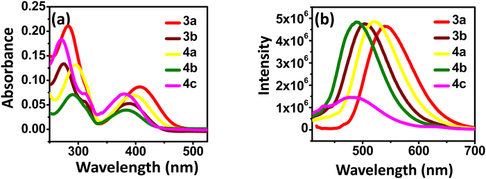 | ||
| Fig. 2 (a) Absorption (10−5 M) and (b) emission spectra (10−7 M) of the compounds 3a–b and 4a–c in DCM. | ||
| Compounds | λ abs (nm) | λ em (nm) | Stokes' shift (nm) | Absorption coefficient (×102 M−1 cm−1) |
|---|---|---|---|---|
| 3a | 282![[thin space (1/6-em)]](https://www.rsc.org/images/entities/char_2009.gif) 406 406 |
539 | 132 | 86.5 |
| 3b | 274![[thin space (1/6-em)]](https://www.rsc.org/images/entities/char_2009.gif) 388 388 |
503 | 115 | 52.7 |
| 4a | 294![[thin space (1/6-em)]](https://www.rsc.org/images/entities/char_2009.gif) 396 396 |
520 | 124 | 69.5 |
| 4b | 290![[thin space (1/6-em)]](https://www.rsc.org/images/entities/char_2009.gif) 384 384 |
488 | 104 | 39.2 |
| 4c | 270![[thin space (1/6-em)]](https://www.rsc.org/images/entities/char_2009.gif) 380 380 |
477 | 97 | 72.1 |
From the observed λmax, methoxy-substituted compounds (3a and 4a) showed higher bathochromic shifts due to their higher donating ability and extended conjugation than other compounds (3b, 4b, 4c).31 The order of the electron-donating property is as follows –OMe > –t-Bu > –CN > –NO2, which correlates with the redshift values.30 A broad emission spectrum was also observed for the compounds in the 450–550 nm region. The highest Stokes shift was observed for compound 3a, which indicates the difference in absorption and emission maximum. Meta-substituted nitro group in compound 4c results in fluorescence quenching as the nitro group is a common fluorescence quencher.32
Electrochemical properties
The compounds' oxidation and reduction potential values are critical parameters for determining the frontier orbitals' energy levels and photophysical parameters. The electrochemical properties of the synthesized compounds 3a–b and 4a–c were studied using cyclic voltammetry. Fig. S18 (ESI†) represents the cyclic voltammograms of the compounds in 10−3 M solution in acetonitrile, and the data is summarised in Table 2.| Compounds | Experimental | Computational | |||||
|---|---|---|---|---|---|---|---|
| E red (V) | E HOMO (eV) | E LUMO (eV) | E g (eV) | E HOMO (eV) | E LUMO (eV) | E g (eV) | |
| 3a | −1.51 | −5.51 | −2.93 | 2.58 | −5.55 | −2.52 | 3.02 |
| 3b | −1.54 | −5.59 | −2.90 | 2.69 | −5.80 | −2.58 | 3.24 |
| 4a | −1.36 | −5.72 | −3.08 | 2.64 | −6.02 | −2.95 | 3.06 |
| 4b | −1.36 | −5.85 | −3.07 | 2.78 | −6.25 | −2.98 | 3.26 |
| 4c | −1.49 | −5.70 | −2.95 | 2.75 | −6.25 | −2.96 | 3.28 |
In all the compounds, benzothiadiazole acts as the significant acceptor moiety. The CV of unsubstituted benzothiadiazole (BTD) shows a one-electron reduction peak near −1.47 V.33 Therefore, the first reduction value of all compounds ranging from −1.35 to −1.51 V is attributed to the BTD group. Noticeably, only a minor change is observed in changing the substituents, which indicates a minimal effect of the substituents in the first reduction potential. When BTD is substituted with electron-withdrawing groups (EWG) such as benzonitrile (4a, 4b) and nitrophenyl (4c), there is a slight positive shift in the values (−1.35 V, −1.46 V) compared to electron-donating groups (EDG) such as t-butylphenyl (3b) and methoxy groups (3a). The presence of EWG makes the BTD core reduction easier. A second irreversible reduction peak is observed in the range of −2.1 V to −2.6 V, possibly due to the further reduction of the benzothiadiazole moiety.
Two oxidation peaks are also observed for the compounds corresponding to the radical cation and radical dication formation.33 The first and second oxidation peaks were observed in a wide range of 1.30 V to 1.75 V and 1.5 V to 2.2 V. This illustrates the strong influence of substituents of BTD in the oxidation process. An increase in oxidation tendency is observed for the high electron donating group. Compound 3a, with a better-donating methoxy group, showed 1st and 2nd oxidation peaks at 1.32 V and 1.53 V, respectively, while compound 3b, with both side t-butyl groups, showed 1st and 2nd oxidation peaks at 1.64 V and 1.84 V respectively. The higher oxidation value of this compound indicates its less stable radical cations.33 A similar trend is observed for compounds 4a–c where both oxidation potential follows the order 4a < 4b < 4c.
The first reduction peak value is considered for calculating the LUMO energy levels using the equation EHOMO/LUMO = − (4.80 − EFerocene + Eoxd/red onset) V.34 The HOMO energy levels were calculated with the help of band gap, which is calculated from absorption edge (1240/λabs). The calculated HOMO and LUMO levels are in the range of −5.51 eV to −5.85 eV & −2.90 eV to −3.08 eV, respectively, which is in accordance with the computational values (Table 2).
Morphology of the thin films and crystal studies
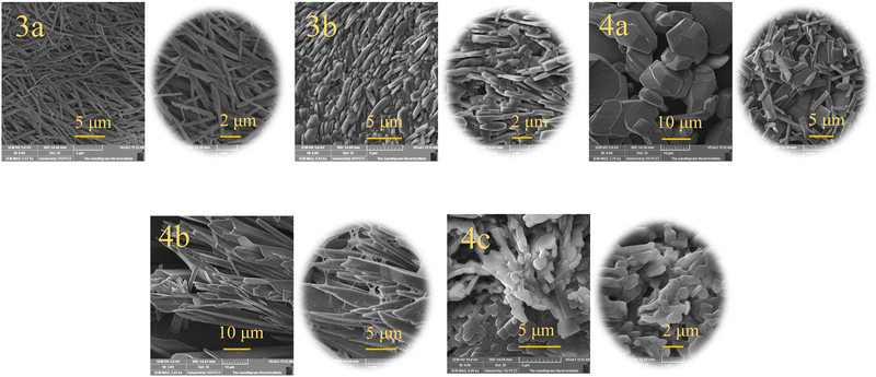
The molecular arrangement in the solid state is a crucial parameter that determines the performance of organic memory devices. The thin film of the all-synthesized compounds was coated over ITO-coated glass plates in chloroform solvent and heated at 80 °C for 20 minutes. Scanning electron microscopic technique (SEM) was used to analyze the surface morphological features. Fig. 3 represents the SEM images of the compounds. All compounds except 4c showed a rod-like structure, while 4c exhibited a microbundles-like close-packed morphology. Achieving uniform coverage in thin films promotes efficient charge transfer across the surface, leading to improved performance and enhanced memory characteristics.Single crystals of compounds 3b and 4b were analyzed on a Bruker Quest (PHOTON III) diffractometer. 3b formed yellow block-shaped crystals while 4b formed yellow plate-shaped crystals after slow evaporation in chloroform: hexane mixture. Both crystals fall under the triclinic crystal system with the P1 space group and have a lamellar arrangement where 3b showed 1D π stacking. In comparison, 4b showed 2D π-stacking in crystal packing (Fig. 4).35Fig. 4 illustrates the crystal structure and packing along with the interactive distance. The compound 3b showed an interactive distance of 2.59 nm between two t-But groups and exhibited direct π–π face interaction along BTD moiety and C–H⋯π edge-to-face interactions near phenyl moiety (Fig. S16, ESI†). In compound 4b, the t-But group interactive distance has reduced to 2.32 nm, and it exhibited more C–H⋯π edge-to-face interactions between the t-But and phenyl groups. It reduced direct π–π face interaction (Fig. S16, ESI†). The C–H⋯π edge-to-face interactions can increase the charge mobility anisotropically, improve the film morphology, and thus reduce threshold voltage.26,36,37
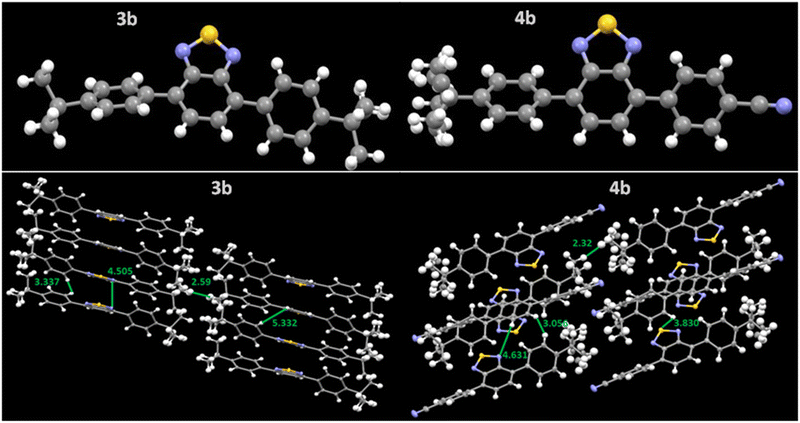 | ||
| Fig. 4 Single crystal structure and packing pattern of the compounds 3b and 4b with their interactive distances (Å). CCDC deposition number(s) 2280971 for 3b and 2280972 for 4b. | ||
Thin-film XRD studies were conducted to investigate the thin-film nature of the compound further (Fig. S17, ESI†). The d-spacing which represents the distance between crystal planes, was calculated using Bragg's law: λ = 2d![[thin space (1/6-em)]](https://www.rsc.org/images/entities/char_2009.gif) sin
sin![[thin space (1/6-em)]](https://www.rsc.org/images/entities/char_2009.gif) θ, where λ is the X-ray wavelength. Across compounds 3a–b and 4a–c, sharp diffraction peaks were observed at 24.90, 5.11, 40.38, 16.48, and 7.96 degrees, indicative of d-spacing values of 3.57, 17.32, 2.23, 5.37, and 11.09 Å, respectively. Notably, 3b and 4c exhibited elevated d-spacing values of 17.32 and 11.09, potentially attributed to the absence of C–H⋯π edge-to-face interactions. On the contrary, compounds 3a, 4a, and 4b displayed smaller d-spacing values, indicating the π–π stacking distance in the compounds.38,39
θ, where λ is the X-ray wavelength. Across compounds 3a–b and 4a–c, sharp diffraction peaks were observed at 24.90, 5.11, 40.38, 16.48, and 7.96 degrees, indicative of d-spacing values of 3.57, 17.32, 2.23, 5.37, and 11.09 Å, respectively. Notably, 3b and 4c exhibited elevated d-spacing values of 17.32 and 11.09, potentially attributed to the absence of C–H⋯π edge-to-face interactions. On the contrary, compounds 3a, 4a, and 4b displayed smaller d-spacing values, indicating the π–π stacking distance in the compounds.38,39
Memory characteristics
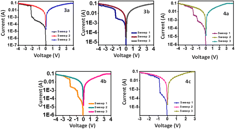
The targeted compounds' resistive memory performance was analyzed by fabricating ITO/3a–b, 4a–c/Ag sandwiched devices. Fig. 5 represents the devices' current vs. voltage plot, which shows the compounds' electrical bistability. The compounds 3a and 3b exhibited binary WORM resistive memory. Ternary WORM memory was observed for compounds 4a and 4b, while 4c exhibited an unusual binary WORM memory.The I–V characteristics of device-based 3a are shown in Fig. 5. Initially, the device was in an OFF state, having a current of 10−5A in the first sweep of −4 V. As the applied negative bias increased, a linear increase in current was observed. However, a sharp increase in current was observed at −1.69 V, which indicates the OFF (HRS) state to ON (LRS) state transition with an ON/OFF of 1.96 × 10². This transition is regarded as the writing process.40 On the subsequent negative and positive sweeps, the device stayed in the ON state. Since it didn't return to the OFF state and showed a retention time of more than 12 hours, it confirms that this device follows binary WORM resistive memory.41 The compound 3b also shows similar binary WORM memory with a smaller threshold voltage of −1.5 V and lower ON/OFF of 2.56 × 101.
The I–V characteristics of device ITO/4a/Ag are represented in Fig. 5. On applying negative bias, an abrupt increase in current was observed at −1.2 V (ON1) and −1.82 V (ON2), resulting in a ternary memory state with ON/OFF of 1.2 × 10². On the subsequent negative and positive sweeps (−4 V and +4 V), the device remained in the ON2 state without transitioning to OFF. This behavior was observed consistently over a retention period exceeding 12 hours. These findings confirm that the device operates based on ternary WORM memory. Compound 4b also showed a similar ternary WORM character with a different ON/OFF ratio of 4.0 × 10² and a low threshold voltage of −0.80 V/−1.79 V. While compound 4c showed unexpected binary WORM memory with ON/OFF of 1.91 × 10⁻² and threshold of −0.80 V. The ON/OFF ratios and threshold voltages of the devices are listed in Table 3.
| Compounds | ON/OFF ratio | Threshold voltage | |
|---|---|---|---|
| V1 | V2 | ||
| 3a | 1.96 × 10² | −1.69 | — |
| 3b | 2.56 × 101 | −1.50 | — |
| 4a | 1.20 × 10² | −1.20 | −1.82 |
| 4b | 4.00 × 10² | −0.80 | −1.79 |
| 4c | 1.91 × 10² | −0.80 | — |
It's worth highlighting that the switching mechanisms are reproducible (Fig. 6). The reproducibility of memory switching was investigated across 20 independent cells of devices 3a–b and 4a–c. Device cells 3a–b displayed binary switching in 67% and 59% of cases, respectively, while 4a–b exhibited ternary switching in 71% and 47% of cells, respectively. Notably, device 4c stood out with an impressive 82% of cells demonstrating binary switching, indicating superior reliability and reproducibility compared to other devices.
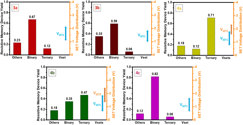 | ||
| Fig. 6 Plot of statistical yield of 20 independent storage cells, VSET distributions are illustrated by an error bar (right in each figure). | ||
Furthermore, the VSET distributions were investigated for 20 independent cells, as illustrated in Fig. 6 by error bars. The VSET voltages for all devices maintained a narrow range, such as 3a, 3b, and 4c operating between −1.1 to −2.2 V, −1.0 to −1.8 V, and −0.7 to −1.7 V, respectively. In the case of Device 4a, the VSET1 and VSET2 voltages fell within the respective ranges of −0.8 to 1.8 V and −1.6 to −2.3 V. Similarly, for Device 4b, VSET1, and VSET2 were observed within the ranges of −0.7 to −1.9 V and −1.4 to −2.4 V, respectively. While all devices exhibited an excellent narrow voltage range, it's worth noting that the VSET1 and VSET2 values for Devices 4a and 4b lacked clear separation. Despite this, the remarkable consistency in the overall narrow VSET distributions across all devices highlights their exceptional repeatability, reinforcing their potential for dependable and stable performance in organic memory devices.42,43
Endurance and retention tests were performed at a constant voltage of 0.5 V for devices 3a, 3b, and 4c, while a continuous bias of −0.25 V & −1 V was used for both 4a and 4b, which showed a ternary character.44 Both the ON and OFF states in the binary devices and ON1, ON2, and OFF states in the ternary devices exhibited no noticeable change during the 1000 seconds in the current vs time retention test and over 100 cycles in the cycle vs current endurance test. The high stability of the devices at different states makes them potential candidates for memory devices. Fig. S23 (ESI†) represents the endurance, and Fig. S24 (ESI†) represents the retention test of all devices. Among all the devices, 4b and 4c showed the lowest threshold voltage of −0.80 V with a high ON/OFF of 4.0 × 10⁻² and 1.91 × 10⁻². Low threshold and high ON/OFF values confirm better device performance of the memory devices.45–48 Since 4c only exhibited binary memory, 4b, which has ternary behavior has the best memory characteristics among the five compounds.
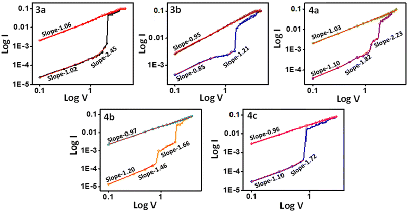
The I–V characteristics obtained were replotted on a log–log scale, as shown in Fig. 7, to understand the memory device behavior. All compounds (3a–b, 4a–c) exhibit ohmic conduction behavior (I ∝ V) at low bias with a slope around one. As the voltage increased, the I ∝ V relation shifted from ohmic to Child law (I ∝ V2) since the slope came near 2. It suggests compounds 3a, 4a, and 4c devices have a space charge limited current (SCLC) as a conduction model49,50 in device 3a. The HRS fitting results showed an initial slope of 1.02, suggesting a high density of charge carriers inside the bulk.51 As the voltage reaches the near-threshold of −1.69 V, the traps will get gradually filled, and as a result, the slope is increased to 2.45. The Fermi level and conduction band get closer, explaining the steady current increase.51 This current is called the trap-free space charge limited current.52 After filling all the traps, an abrupt increase in the current is observed at −1.69 V, leading to the ON state of the device. At the ON state, the curve shows a slope of 1.06, corresponding to the ohmic conductance, thus leading to an efficient channel for charge carrier transport.53 Device 4c also shows similar trends. Device 4a showed a ternary behavior. As a result, it has an intermediate state with a slope of 2.23, also following the Child's law, indicating the SCLC mechanism. On further increase in voltage, the device reaches the ON2 state, which follows ohmic conduction with a slope of 1.03.54 On the other hand, 3b and 4b initially exhibited ohmic conduction with a linear relation with current and voltage, and as the voltage increased, it displayed Pool–Frenkel-type conduction instead of following the Child's square law.55
Memory switching mechanism
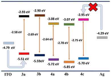
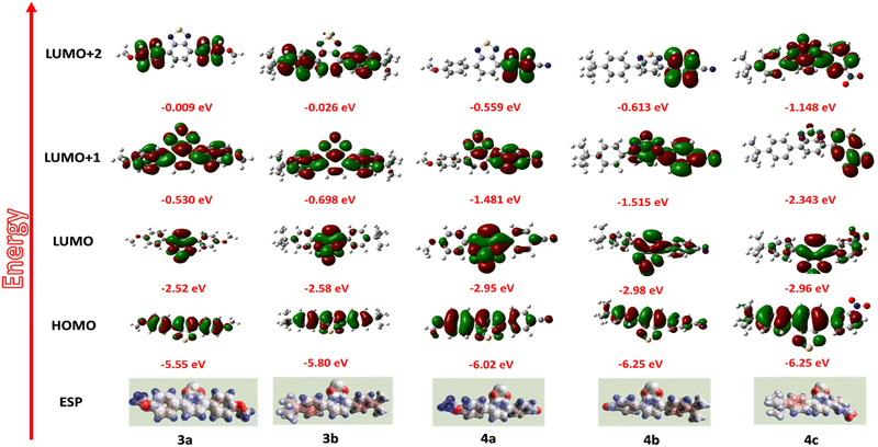
To better understand the mechanism, the HOMO–LUMO energy level diagrams are compared with the electrode energy levels (Fig. 8). A clear-cut increase in the HOMO levels of 3a–b is observed due to the high donating capacity of two methoxy and t-Bu groups. On the other hand, introducing electron-withdrawing groups such as –CN and –NO2 considerably decreases the LUMO energy levels. On comparing the energy barrier between the electrodes and frontier orbitals of the compounds, the hole injection from ITO (−4.79 eV)56 to HOMO (−5.51 to 5.85 eV) levels have a lower energy barrier compared to the electron injection from Ag (−4.29 eV)57 to LUMO (−2.90 to 3.07 eV) levels. Hence, hole injection dominates over electron injection in the active layer.58,59For a deeper understanding of the mechanism, molecular simulations of the compounds were investigated (Fig. 9). For compounds 3a and 3b, the HOMO levels are distributed along the molecule's backbone. Still, the LUMO level electron density is present at the benzothiadiazole moiety, indicating a possible intramolecular charge transfer.60,61 The redistribution of electron density to the whole molecular backbone is seen in the LUMO+1 and LUMO+2 states, avoiding the possibility of another ICT mechanism. So, compounds 3a and 3b only show binary switching due to the presence of only one acceptor moiety (BTD) for charge transfer.62 For compounds 4a, 4b, and 4c, the electron density is present throughout the molecular backbone. A shift of electron density to the acceptor side (BTD-CN/BTD-NO2) is observed in the LUMO levels, which guarantees the ICT from the electron donor (OMe, t-But) side to the acceptor (BTD-CN/BTD-NO2), resulting in the first switching. The charge distribution is maintained in the LUMO+1 but is again redistributed in LUMO+2 for compounds 4a–b.63 This suggests the other charge transfer process and explains the high performance of 4a and 4b showing ternary WORM memory behavior.64 The high dipole moment of compound 4a–c (7.327, 6.819, 5.437) explains the high retention time of the compound, which is up to 24 hours. The high dipole moment increases the retention time by stabilizing the charge transfer state.50,65,66 The CV data presented in Fig. S18 (ESI†) supports the discussions above. The irreversible anode peak in all compounds indicates the high stability of their oxidation state. Consequently, the excited electron is less likely to revert to the HOMO levels, substantiating the non-volatile behavior observed in compounds 3a–b and 4a–c.67 Compound 4c's unexpected binary switching is due to the poor thin film formation, which is proved through the SEM analysis showing microbundle-like morphology different from others.
The MESP (Merz–Kollman potential) images reveal that the compounds exhibit a consistent positive charge throughout (depicted by the blue region), creating a continuous pathway for charge carriers (Fig. 9).68,69 However, certain areas in the compounds (highlighted in red) can act as a trap, hindering the smooth flow of charge conduction. These traps are formed by acceptor units (BTD, NO2, CN), and their depth increase as the strength of the acceptor increases.70 On applying an external voltage, the holes will accumulate in the traps, requiring additional bias to facilitate the charge transition. The first switching happens when the bias equals the threshold voltage (−0.80 to 1.69 V). The ICT mechanism further stabilizes the trapped charges. Despite applying a reverse voltage sweep, the trapped charges remain persistent and cannot be easily removed. Consequently, they play a crucial role in establishing a stable low resistance state, exhibiting non-volatile WORM memory behavior.50 Also, not all traps within the compounds fill simultaneously due to variations in trap strength. As a consequence, compounds 4a and 4b, which incorporate two different acceptors, exhibit distinct switching and show ternary resistive switching.70
Hence, the memory behavior of compounds can be attributed to a combination of charge transfer and charge trapping mechanisms. This interplay between charge transfer and charge trapping contributes to the characteristic switching behavior observed in the compounds, facilitating WORM memory.50,62 The compound 4b, with a moderate band gap of −2.48 eV exhibited the best memory performance with the lowest threshold voltage of −0.80 V and the highest ON/OFF of 4 × 10². By substituting the t-Bu group, the thin film formation also remarkably improved.61 So, devices that exhibit a better thin film and balanced charge distribution between the donor and acceptor tend to possess enhanced properties. Therefore, employing molecular designs that incorporate donors and acceptors with equivalent strength is advantageous. This balanced approach ensures optimal performance and enhances the overall functionality of the devices.
Conclusion
Five novel organic small molecules centered on a benzothiadiazole (BTD) core were strategically designed and synthesized, embracing the D–A–D and D–A–A architectures. The synthesized molecules were characterized using 1H-NMR, 13C-NMR, and HRMS techniques. Notably, these compounds exhibited commendable solubility across a spectrum of organic solvents, presenting a favorable attribute for the fabrication of solution-based organic memory devices. All the compounds exhibited excellent semiconductor behavior, with calculated band gaps ranging from −2.90 eV to −3.08 eV based on photophysical and electrochemical data analysis. The frontier orbitals of the compounds were finely tuned by introducing different substituents to the BTD moiety. The compounds' crystalline nature and thin film properties were investigated using SEM, single crystal XRD, and thin film XRD, revealing that all compounds, except the compound with NO2/t-Bu unsymmetrical substitution, displayed good surface coverage and a rod-like structure in the thin film. The compound with CN/t-Bu substituted unsymmetrically has exhibited more C–H⋯π edge-to-face interactions between the t-But group and phenyl group and reduced direct π–π face interactions, thereby enhancing thin film forming and charge carrier mobilities. The strategic transition from the D–A–D to the D–A–A architecture engendered a transformative shift from binary WORM memory to ternary WORM memory. Notably, incorporating the acceptor molecule in compounds OMe/CN unsymmetrical and t-Bu/CN unsymmetrical compounds facilitated the emergence of a secondary charge trap, facilitating additional charge transfer transitions. All the devices exhibited an an electrical bistability with an ON/OFF ratio ranging from 101–102. Devices with OMe/CN unsymmetrical and t-Bu/NO2 unsymmetrical substitutions demonstrated superior reproducibility, with 71% and 82% of cells exhibiting ternary and binary switching, respectively, outperforming other devices. All devices demonstrated a consistent and narrow VSET voltage range, underscoring their remarkable repeatability. The memory switching mechanism, elucidated through the HOMO/LUMO and MESP diagram analysis, was attributed to the combined effect of charge transfer and trapping. Among the compounds, t-Bu/CN unsymmetrical compound exhibited superior memory performance with a low threshold voltage (−0.80 V) and a high ON/OFF ratio (102). The substitution of t-Bu and cyano groups in this compound facilitated an enhanced charge transfer mechanism, owing to their moderate donor–acceptor strength and band gap.Author contributions
Bhagyanath P K: synthesis, methodology, data curation, data interpretation, design, and writing – original draft, Varghese M. Angela: supervision, review and editing, Asit Hait: methodology and writing, Pradhanekar M. Imran: computational analysis. Nattamai. S. P. Bhuvanesh: single-crystal XRD analysis, Samuthira Nagarajan: project administration, design, supervision, review, and editing.Conflicts of interest
There are no conflicts to declare.Acknowledgements
The authors acknowledge the Central University of Tamil Nadu for the research facilities.Notes and references
- A. Seabaugh, IEEE Spectrum, 2013, 50, 35–62 Search PubMed
.
- H. Li, Q. Xu, N. Li, R. Sun, J. Ge, J. Lu, H. Gu and F. Yan, J. Am. Chem. Soc., 2010, 132, 5542–5543 CrossRef CAS PubMed
.
- K. D. M. Rao, A. A. Sagade, R. John, T. Pradeep and G. U. Kulkarni, Adv. Electron. Mater., 2016, 2, 1500286 CrossRef
.
- R. Gupta, P. Jash and P. C. Mondal, J. Mater. Chem. C, 2021, 9, 11497–11516 RSC
.
- Y. Li, Q. Qian, X. Zhu, Y. Li, M. Zhang, J. Li, C. Ma, H. Li, J. Lu and Q. Zhang, InfoMat, 2020, 2, 995–1033 CrossRef CAS
.
- Y. Li, Q. Qian, S. Ling, T. Fan, C. Zhang, X. Zhu, Q. Zhang, Y. Zhang, J. Zhang, S. Yu, J. Yao and C. Ma, J. Solid State Chem., 2021, 294, 121850 CrossRef CAS
.
- H. Li, Z. Jin, N. Li, Q. Xu, H. Gu, J. Lu, X. Xia and L. Wang, J. Mater. Chem., 2011, 21, 5860 RSC
.
- H. Liu, H. Zhuang, H. Li, J. Lu and L. Wang, Phys. Chem. Chem. Phys., 2014, 16, 17125–17132 RSC
.
- K. Zhao, F. Yu, W. Liu, Y. Huang, A. A. Said, Y. Li and Q. Zhang, J. Org. Chem., 2020, 85, 101–107 CrossRef CAS PubMed
.
- H. Zhuang, Q. Zhang, Y. Zhu, X. Xu, H. Liu, N. Li, Q. Xu, H. Li, J. Lu and L. Wang, J. Mater. Chem. C, 2013, 1, 3816 RSC
.
- H. Liu, H. Zhuang, H. Li, J. Lu and L. Wang, Phys. Chem. Chem. Phys., 2014, 16, 17125–17132 RSC
.
- B. A. D. Neto, A. A. M. Lapis, E. N. Da Silva Júnior and J. Dupont, Eur. J. Org. Chem., 2013, 228–255 CrossRef CAS
.
- F. Gozzo, J. Agric. Food Chem., 2003, 51, 4487–4503 CrossRef CAS PubMed
.
- S. Mataka, K. Takahashi, T. Imura and M. Tashiro, J. Heterocycl. Chem., 1982, 19, 1481–1488 CrossRef CAS
.
- T. Balasankar, M. Gopalakrishnan and S. Nagarajan, Eur. J. Med. Chem., 2005, 40, 728–731 CrossRef CAS PubMed
.
- M. Witvrouw, C. Pannecouque, K. Van Laethem, J. Desmyter, E. De Clercq and A.-M. Vandamme, AIDS, 1999, 13, 1478 CrossRef PubMed
.
- T. C. Parker, D. G. (Dan) Patel, K. Moudgil, S. Barlow, C. Risko, J.-L. Brédas, J. R. Reynolds and S. R. Marder, Mater. Horiz., 2015, 2, 22–36 RSC
.
- I. Bala, R. A. K. Yadav, M. Devi, J. De, N. Singh, K. Kailasam, J. Jayakumar, J.-H. Jou, C.-H. Cheng and S. K. Pal, J. Mater. Chem. C, 2020, 8, 17009–17015 RSC
.
- J. Cameron, L. Nanson, N. Blouin, N. J. Findlay, A. R. Inigo and P. J. Skabara, Org. Electron., 2017, 49, 400–405 CrossRef CAS
.
- R. Cui, Y. Zou, L. Xiao, C.-S. Hsu, M. L. Keshtov, D. Yu. Godovsky and Y. Li, Dyes Pigm., 2015, 116, 139–145 CrossRef CAS
.
- M. Godfroy, J. Liotier, V. M. Mwalukuku, D. Joly, Q. Huaulmé, L. Cabau, C. Aumaitre, Y. Kervella, S. Narbey, F. Ostwald, E. Palomares, C. A. González Flores, G. Oskam and R. Demadrille, Sustainable Energy Fuels, 2021, 5, 144–153 RSC
.
- Y. Li, C. Zhang, Z. Shi, J. Li, Q. Qian, S. Ling, Y. Zhang, X. Zhu, X. Wu, J. Zhang, R. Zhao, Y. Jiang, Q. Zhang and C. Ma, Coatings, 2021, 11, 318 CrossRef CAS
.
- Y.-H. Cheng, H.-L. Wong, E. Y.-H. Hong, M.-Y. Leung, S.-L. Lai and V. W.-W. Yam, ACS Mater. Lett., 2020, 2, 1590–1597 CrossRef CAS
.
- X. Lin, Q. Lu, C. Yang, Y. Wang, W. Zhang, D. Li, Y. Gao, H. Niu and W. Wang, J. Mater. Sci., 2021, 56, 12001–12017 CrossRef CAS
.
- Z. He, H. Xu, Y. Zhang, Y. Hou and H. Niu, Polymers, 2022, 14, 4965 CrossRef CAS
.
- J. Han, H. Lian, X. Cheng, Q. Dong, Y. Qu and W. Wong, Adv. Electron. Mater., 2021, 7, 2001097 CrossRef CAS
.
- P. Rietsch, S. Sobottka, K. Hoffmann, A. A. Popov, P. Hildebrandt, B. Sarkar, U. Resch-Genger and S. Eigler, Chem. – Eur. J., 2020, 26, 17361–17365 CrossRef CAS
.
- D. Gudeika, A. Miasojedovas, O. Bezvikonnyi, D. Volyniuk, A. Gruodis, S. Jursenas and J. V. Grazulevicius, Dyes Pigm., 2019, 166, 217–225 CrossRef CAS
.
- A. Anjali, R. Dheepika, P. M. Imran, N. S. P. Bhuvanesh and S. Nagarajan, ACS Appl. Electron. Mater., 2020, 2, 2651–2661 CrossRef CAS
.
- K. M. Omer, S. Y. Ku, K. T. Wong and A. J. Bard, J. Am. Chem. Soc., 2009, 131, 10733–10741 CrossRef CAS
.
- P. Rietsch, S. Sobottka, K. Hoffmann, A. A. Popov, P. Hildebrandt, B. Sarkar, U. Resch-Genger and S. Eigler, Chem. – Eur. J., 2020, 26, 17361–17365 CrossRef CAS
.
- C. X. Zhao, T. Liu, M. Xu, H. Lin and C. J. Zhang, Chin. Chem. Lett., 2021, 32, 1925–1928 CrossRef CAS
.
- K. M. Omer, S. Y. Ku, K. T. Wong and A. J. Bard, J. Am. Chem. Soc., 2009, 131, 10733–10741 CrossRef CAS PubMed
.
- Y. Li, C. Zhang, Z. Shi, J. Li, Q. Qian, S. Ling, Y. Zhang, X. Zhu, X. Wu, J. Zhang, R. Zhao, Y. Jiang, Q. Zhang and C. Ma, Coatings, 2021, 11, 318 CrossRef CAS
.
- K. Zhou, H. Dong, H. Zhang and W. Hu, Phys. Chem. Chem. Phys., 2014, 16, 22448–22457 RSC
.
- J. Keruckas, D. Volyniuk, J. Simokaitiene, E. Narbutaitis, A. Lazauskas, P.-H. Lee, T.-L. Chiu, C.-F. Lin, P. Arsenyan, J.-H. Lee and J. V. Grazulevicius, Org. Electron., 2019, 73, 317–326 CrossRef CAS
.
- M. Uno, T. Uemura, Y. Kanaoka, Z. Chen, A. Facchetti and J. Takeya, Org. Electron., 2013, 14, 1656–1662 CrossRef CAS
.
- Y. Li, H. Li, H. Chen, Y. Wan, N. Li, Q. Xu, J. He, D. Chen, L. Wang and J. Lu, Adv. Funct. Mater., 2015, 25, 4246–4254 CrossRef CAS
.
- P.-L. T. Boudreault, J. W. Hennek, S. Loser, R. P. Ortiz, B. J. Eckstein, A. Facchetti and T. J. Marks, Chem. Mater., 2012, 24, 2929–2942 CrossRef CAS
.
- R. Bo, H. Li, H. Liu, H. Zhuang, N. Li, Q. Xu, J. Lu and L. Wang, Dyes Pigm., 2014, 109, 155–162 CrossRef CAS
.
- J.-H. Wu and G.-S. Liou, ACS Appl. Mater. Interfaces, 2015, 7, 15988–15994 CrossRef CAS PubMed
.
- Y. Li, Y. Pan, C. Zhang, Z. Shi, C. Ma, S. Ling, M. Teng, Q. Zhang, Y. Jiang, R. Zhao and Q. Zhang, ACS Appl. Mater. Interfaces, 2022, 14, 44676–44684 CrossRef CAS PubMed
.
- Z. He, X. Chen, H. Yu, Y. Du, M. Gao, S. Wang and C. Wang, Chem. Eng. J., 2023, 457, 141365 CrossRef CAS
.
- C. Wang, B. Hu, J. Wang, J. Gao, G. Li, W.-W. Xiong, B. Zou, M. Suzuki, N. Aratani, H. Yamada, F. Huo, P. S. Lee and Q. Zhang, Chem. – Asian J., 2015, 10, 116–119 CrossRef PubMed
.
- Z. Xing, Y. Wang, Y. Han, Y. Zhai, Y. Tian, S. Qi, X. Zhu, Z. Jiang and Z. Chen, Dyes Pigm., 2021, 189, 109259 CrossRef CAS
.
- Q. Liu, L.-X. Jin and J.-F. Lu, J. Mol. Struct., 2021, 1228, 129480 CrossRef CAS
.
- H. Cao, Q. Zhang, H. Li and J. Lu, J. Mater. Chem. C, 2021, 9, 569–574 RSC
.
- G. Wang, Q. Zhang, F. Zhu, C. Zhang, H. Li and J. Lu, J. Mater. Chem. C, 2021, 9, 6351–6356 RSC
.
- Y. Qi, Z. Shen, C. Zhao and C. Z. Zhao, J. Alloys Compd., 2020, 822, 153603 CrossRef CAS
.
- D. Harshini, V. M. Angela, P. Devibala, P. M. Imran, N. S. P. Bhuvanesh and S. Nagarajan, ACS Appl. Electron. Mater., 2022, 4, 4383–4395 CrossRef CAS
.
- Y. C. Yang, F. Pan, Q. Liu, M. Liu and F. Zeng, Nano Lett., 2009, 9, 1636–1643 CrossRef CAS PubMed
.
- T. H. Hou, K. L. Lin, J. Shieh, J. H. Lin, C. T. Chou and Y. J. Lee, Appl. Phys. Lett., 2011, 10, 98 Search PubMed
.
- F. C. Chiu, H. W. Chou and J. Y. M. Lee, J. Appl. Phys., 2005, 10, 97 Search PubMed
.
- Y. Li, Q. Qian, S. Ling, T. Fan, C. Zhang, X. Zhu, Q. Zhang, Y. Zhang, J. Zhang, S. Yu, J. Yao and C. Ma, J. Solid State Chem., 2021, 294, 121850 CrossRef CAS
.
- L. Wu, C. Dong, X. Wang, J. Li and M. Li, J. Alloys Compd., 2019, 779, 794–799 CrossRef CAS
.
- J.-H. Li, Y. Li, J.-T. Xu and C. K. Luscombe, ACS Appl. Mater. Interfaces, 2017, 9, 17942–17948 CrossRef CAS PubMed
.
- M. U. Khan, G. Hassan and J. Bae, Appl. Phys. A: Mater. Sci. Process., 2019, 125, 378 CrossRef
.
- J. Liu, F. Yang, L. Cao, B. Li, K. Yuan, S. Lei and W. Hu, Adv. Mater., 2019, 31, 1902264 CrossRef PubMed
.
- J. Han, H. Lian, X. Cheng, Q. Dong, Y. Qu and W. Wong, Adv. Electron. Mater., 2021, 7, 2001097 CrossRef CAS
.
- Q. Liu, C. Zhao, G. Tian and H. Ge, RSC Adv., 2018, 8, 805–811 RSC
.
- J. Han, H. Lian, X. Cheng, Q. Dong, Y. Qu and W. Wong, Adv. Electron. Mater., 2021, 7, 2001097 CrossRef CAS
.
- V. M. Angela, D. Harshini, A. Anjali, P. M. Imran, N. S. P. Bhuvanesh and S. Nagarajan, Chem. – Eur. J., 2022, 8, e202202569 Search PubMed
.
- J.-H. Wu and G.-S. Liou, ACS Appl. Mater. Interfaces, 2015, 7, 15988–15994 CrossRef CAS
.
- Y. Li, C. Zhang, Z. Shi, J. Li, Q. Qian, S. Ling, Y. Zhang, X. Zhu, X. Wu, J. Zhang, R. Zhao, Y. Jiang, Q. Zhang and C. Ma, Coatings, 2021, 3, 11–318 Search PubMed
.
- Q. Zhang, J. He, H. Li, N. Li, Q. Xu, D. Chen and J. Lu, J. Mater. Chem. C, 2017, 5, 7961–7968 RSC
.
- S. Miao, H. Li, Q. Xu, Y. Li, S. Ji, N. Li, L. Wang, J. Zheng and J. Lu, Adv. Mater., 2012, 24, 6210–6215 CrossRef CAS PubMed
.
- H. Yu, H. Liu, H. Tan, H. Yao, Y. Song, S. Zhu, N. Song, B. Zhang and S. Guan, Dyes Pigm., 2018, 158, 97–103 CrossRef CAS
.
- S. Gao, X. Yi, J. Shang, G. Liu and R.-W. Li, Chem. Soc. Rev., 2019, 48, 1531–1565 RSC
.
- C.-T. Poon, D. Wu, W. H. Lam and V. W.-W. Yam, Angew. Chem., Int. Ed., 2015, 54, 10569–10573 CrossRef CAS PubMed
.
- Y. Li, Q. Qian, S. Ling, T. Fan, C. Zhang, X. Zhu, Q. Zhang, Y. Zhang, J. Zhang, S. Yu, J. Yao and C. Ma, J. Solid State Chem., 2021, 294, 121850 CrossRef CAS
.
Footnote |
| † Electronic supplementary information (ESI) available. CCDC 2280971 and 2280972. For ESI and crystallographic data in CIF or other electronic format see DOI: https://doi.org/10.1039/d4ma00068d |
| This journal is © The Royal Society of Chemistry 2024 |


