
 Open Access Article
 This Open Access Article is licensed under a
 Creative Commons Attribution 3.0 Unported Licence
Porous aluminum decorated with rhodium nanoparticles: preparation and use as a platform for UV SERS†
Shrobona
Banerjee
ab,
Luca
Mattarozzi
c,
Nicolò
Maccaferri
d,
Sandro
Cattarin
 c,
Shukun
Weng
a,
Ali
Douaki
a,
German
Lanzavecchia
a,
Anastasiia
Sapunova
a,
Francesco
D'Amico
e,
Qifei
Ma
ag,
Yanqiu
Zou
ah,
Roman
Krahne
a,
Janina
Kneipp
b and
Denis
Garoli
*afg
c,
Shukun
Weng
a,
Ali
Douaki
a,
German
Lanzavecchia
a,
Anastasiia
Sapunova
a,
Francesco
D'Amico
e,
Qifei
Ma
ag,
Yanqiu
Zou
ah,
Roman
Krahne
a,
Janina
Kneipp
b and
Denis
Garoli
*afg
aIstituto Italiano di Tecnologia, via Morego 30, I-16163, Genova, Italy. E-mail: denis.garoli@unimore.it
bHumboldt-Universität zu Berlin, Brook-Taylor-Straße 2, 12489 Berlin, Germany
cICMATE – CNR, Corso Stati Uniti 4, 35127 Padova, Italy
dDepartment of Physics, Umeå University, Linnaeus väg 24, 901 87 Umeå, Sweden
eElettra Sincrotrone Trieste S.C.p.A., S.S. 14 km 163,5 in Area Science Park, 34149, Basovizza, TS, Italy
fDipartimento di Scienze e Metodi dell’Ingegneria, Università degli Studi di Modena e Reggio Emilia, Via Amendola 2, 42122, Reggio Emilia, Italy
gCollege of Optical and Electronic Technology, China Jiliang University, Hangzhou, 310018, China
hState Key Laboratory of Modern Optical Instrumentation, College of Optical Science and Engineering, Zhejiang University, Hangzhou 310027, China
First published on 25th June 2024
Abstract
Currently, there is a high interest in novel plasmonic platforms and materials able to extend their applicability into the ultraviolet (UV) region of the electromagnetic spectrum. In the UV it is possible to explore the spectral properties of biomolecules that have only a small cross-section in the visible spectral range. However, most plasmonic metals have their resonances at wavelengths >350 nm. Aluminum and rhodium are two exceptions and therefore interesting candidate materials for UV plasmonics. In this work we developed a simple and low-cost preparation of functional substrates based on nanoporous aluminum decorated with rhodium nanoparticles. We demonstrate that these functionalized nanoporous metal films can be exploited as plasmonic materials for enhanced UV Raman spectroscopy.
Introduction
Plasmonics was born in the 1950s, with the discovery of grating anomalies by Wood. After this, the excitation of surface plasmon polaritons (SPPs) by randomly rough surfaces initiated fascinating topics in modern physics like enhanced backscattering or Anderson localization of photons. Then, plasmonics went through a novel resurgence in research in the mid-1970s when surface-enhanced Raman scattering (SERS) was discovered.1–3 Ultimately, in the last two decades a new boom of plasmonics and its applications has occurred. Nowadays surface plasmon resonance finds extensive applications in SERS, metal-enhanced fluorescence (MEF), photocatalysis, optical trapping, heating, etc.2 Thanks to the innovation in fabrication techniques and spectroscopic methods, localized surface plasmon resonance (LSPR) can be applied in multiple spectral regions. The most used noble metals (Au and Ag) are typically applied in the visible/near-infrared (Vis/NIR), while metals such as aluminum, magnesium, rhodium and gallium can be used to extend the spectral range to higher energy (into UV and deep-UV wavelengths).4,5 The excitation of biomolecules using UV radiation is particularly interesting for Raman spectroscopy. In fact, most biomolecules have small Raman cross-sections in the visible and NIR regions,6,7 and the use of higher energy to excite them can increase the detection limit due to the presence of electronic resonances.8–12 Aluminum (Al) is the most extensively explored material for UV plasmonics.13 In order to use Al to generate LSPR in the UV spectral region, very small metallic features/nanostructures must be prepared by means of advanced lithographic techniques or by means of chemical synthesis of nanoparticles.14–16 As an alternative approach to produce nanostructured metals, the preparation of Al films as nanoporous materials (NPMs) has been recently reported.7,17,18 During the last decade, NPMs have attracted increasing interest due to their unique very high specific surface area, and their applications in multiple fields is extensively documented.19–22 We know that porous Al (as a metal with low oxygen content) structures can be prepared by means of a galvanic displacement (GD) reaction or electrochemical dealloying, respectively, starting from an alloy of Mg3Al2.7,23 GD is an electroless wet deposition technique that may be used with a simple chemical apparatus to deposit metallic dots or thin layers of a more noble metal spontaneously, in an open circuit. The approach is applicable with apparent advantages: (i) metallic or semiconducting substrates of complex geometry, as the solution may creep into recessed but connected empty volumes; (ii) topologies like patterned planar substrates, as the procedure may skip the application of masks. Due to these advantages, it is the object of intense current investigation.24In our case, a metal of low redox potential (E) like Al25 oxidizes and dissolves
| Al3+ + 3e− → Al E° = −1.662 V |
| Rh3+ + 3e− → Rh E° = 0.758 V |
| Al + Rh3+ → Al3+ + Rh |
As previously mentioned, rhodium (Rh) is an interesting candidate metal for UV plasmonics and examples of its use for enhanced spectroscopies have been reported.8,26–29 The current main limitation in the use of Rh in the preparation of nanostructures is its very high cost. Therefore, alternative low cost approaches are sought. Also, the combination of two plasmonic metals in the same platform can, in principle, provide more tunable optical properties and better field enhancement for spectroscopic applications.30,31
In this paper, we discuss the facile and low-cost preparation of porous Al films decorated with Rh nanoparticles with increasing surface coverage density. In view of the potential application as a UV plasmonic platform we tested the films for SERS using an excitation wavelength of 266 nm to probe the adenine molecules deposited, via physical vapor deposition, on the surface. The results are discussed with the support of numerical simulations to rationalize the observed trend in Raman signal intensities.
Results and discussion
The morphology of porous Al samples decorated with Rh nuclei on the surface, obtained by a galvanic displacement process, was characterized by scanning electron microscopy (SEM) and atomic force microscopy (AFM). Merely etched samples (Fig. 1a and ESI,† Fig. S1–S6) show a strongly roughened/porous Al surface with features of a size of a few to several microns, presumably reflecting the metallic grain structure. Upon galvanic displacement, randomly distributed Rh nanoparticles appear (Fig. 1b-c-c′), with a morphology approaching a spherical or crushed spherical shape. Moreover, for a given Rh3+ concentration, with increasing time of treatment tGD, a rise in the number of particles and their average dimensions was observed, reaching typical diameters in the range of 100–300 nm for tGD = 2 min. On the other hand, exposing Al surfaces to different Rh3+ concentrations for the same time of tGD = 1 min (samples b and f in Table 1), the sample f exposed to the larger [Rh3+] shows a much larger density of nucleated particles, and a limited increase in their average dimensions, as the particles tend to approach overlapping and complete substrate coverage (AFM maps are reported in the ESI,† Fig. S7–S11).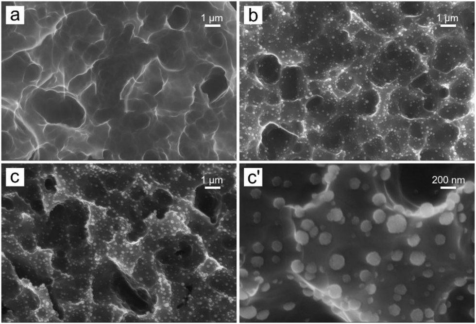 | ||
| Fig. 1 SEM images of (a) untreated porous Al (sample a, no GD) and b-c-c′ (porous Al samples subjected to galvanic displacement) in 0.5 mM Na3RhCl6, pH 2.0, for different times: (b) tGD = 1 min (sample b); (c) tGD = 2 min (sample c); (c′) tGD = 2 min, magnified detail. | ||
| Sample | GD bath | t GD/min | Rh at% (EDS) |
|---|---|---|---|
| (a) | No treatment | — | — |
| (b) | 0.5 mM Na3RhCl6 + 0.09 M NaCl | 1 | 0.23–0.29 |
| (c) | 0.5 mM Na3RhCl6 + 0.09 M NaCl | 2 | 0.43–0.54 |
| (d) | 0.5 mM Na3RhCl6 + 0.09 M NaCl | 4 | 0.93–1.16 |
| (e) | 0.5 mM Na3RhCl6 + 0.09 M NaCl | 6 | 1.24–1.32 |
| (f) | 2.0 mM Na3RhCl6 + 0.09 M NaCl | 1 | 1.48–1.53 |
Values of Rh at% reported in Table 1 were obtained as panoramic averaged values, at ×1000 magnification, and do not provide a reliable quantitative analysis due to the inhomogeneous depth profile of the samples. However, samples from b to e show a significant qualitative trend of increasing Rh content with increasing time of GD treatment. Data from the last sample f show that the bath containing 2.0 mM Na3RhCl6 concentration causes a rather fast deposition, somewhat difficult to control and standardize.
The basic optical properties of the samples were then explored by reflectance measurements using an integrating sphere to collect the total reflectance from the highly rough samples. The results, reported in the ESI,† Fig. S12, showed the expected interband transition of Al at around 800 nm for all the samples, while increasing RhNP content showed additional spectral features at around 240 nm.
Building on previous studies that have demonstrated the potential of nanoporous aluminum (NPA) to function as plasmonic substrates, particularly for SERS,23 the rhodium nanoparticle-coated NPA described here was used in Raman experiments excited at a wavelength of 266 nm. Adenine was chosen as an analyte, as its strong absorption near the excitation wavelength can lead to additional electronic resonance enhancement of the Raman spectra.32–34
Adenine spectra obtained from all the samples are shown in Fig. 2. All show clearly distinguishable bands that correspond to the molecular vibrations of adenine as reported previously in resonant Raman experiments with adenine and related compounds,35–37 as well as in pre-resonant SERS spectra of Rh composite materials.38,39
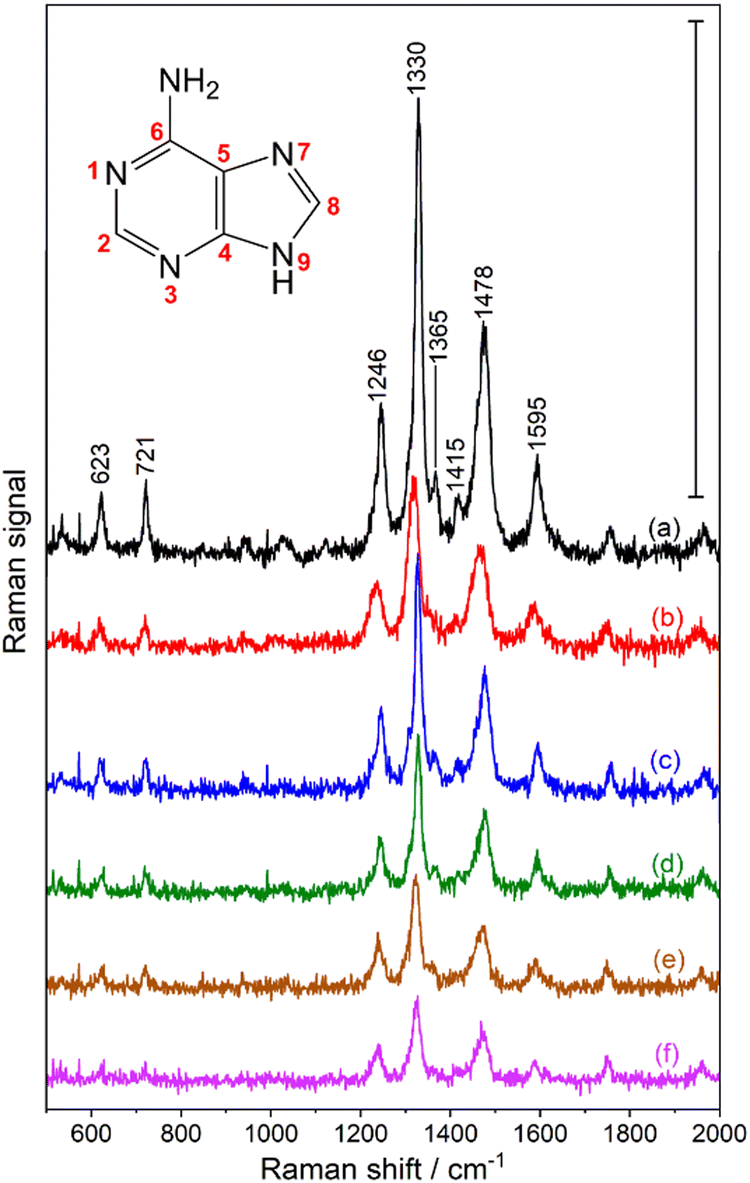 | ||
| Fig. 2 Averages of 6 spectra collected over 30 minutes for samples (a)–(f) defined in Table 1: (a) untreated porous Al; and (b)–(f) samples of Rh-decorated porous Al. Scale bar corresponds to 1 count per second (cps). Acquisition time per spectrum: 300 s, excitation wavelength: 266 nm, excitation intensity: 3.8 W cm−2. | ||
All observed bands are listed in Table 2, and the inset in Fig. 2 shows numbering of the atoms referred to in the assignment table. The skeletal vibrations corresponding to the six-membered pyrimidine ring (1592 cm−1 and 1474 cm−1),36,40,41 and the five-membered imidazole (1330 cm−1) indicate that the purine structure of the adenine molecules remains intact during the thermal evaporation procedure that was used to deposit the molecule onto the substrate. This band dominates the spectra, in agreement with previous work discussing a charge transfer-based chemical enhancement of this mode for adenine adsorbed on Rh under pre-resonant conditions.38 The amino group is represented by the pronounced C6–NH2 stretching vibration at 1246 cm−1, also in agreement with previous works.32,36,40,41 The spectrum shows similarities but also differs slightly from spectra of adenine that were observed for adenine films on other Al substrates that did not contain Rh nanostructures.16
| Raman band (cm−1) | Tentative assignment | Ref. |
|---|---|---|
| 622 | Ring deformations C4–C5–N7, C4–C5–C6 | 41 |
| 721 | Purine ring breathing | 37 |
| 1246 | Stretching C6–NH2, C–N7; rocking NH2 | 36 and 40 |
| 1330 | Stretching C5–N7, N1–C2; bending C2–H, C8–H | 41 |
| 1365 | Stretching C8–N9, C4–N9; bending C2–H, N9–H | 36 and 41 |
| 1415 | Stretching C4–N9, C8–N7, C6–N1 | 37 and 41 |
| 1478 | Scissoring NH2; e1u of six-membered ring (pyridine) | 36, 40 and 41 |
| 1595 | Scissoring NH2; e2g of six-membered ring (pyridine) | 36 and 41 |
Considering the small amount of analyte in the few-nm layer that is deposited, the porous aluminum substrate could serve as an efficient optical substrate that can carry small analyte amounts at its enlarged surface, and more importantly, could provide optimal plasmonic properties for potential SERS enhancement38,42–46 as well. In order to investigate the influence of the presence of the rhodium nanostructures (Fig. 1) on its properties as a substrate for Raman experiments, the observed signal intensities can be compared. Interestingly, the overall signal intensity decreases for substrates containing higher proportions of RhNP (Fig. 2b–f), and the control sample that does not contain any rhodium nanoparticles (Fig. 2a) shows the highest signal. We attribute the observed decreasing intensity to different effects. The effect of such a photodegradation has been reported on other Al substrates previously.16
Firstly, while the NPA substrate itself may provide advantageous plasmonic properties for SERS enhancement,23 it also provides a large available surface to the molecules. The presence of the Rh nanoparticles and their favorable possibilities of a chemical SERS enhancement38 are ‘outweighed’ by the decreasing available surface on the aluminum substrate. In principle, adding RhNPs on top of the NPA film, the surface area should increase, and stronger signal should be observed. In contrast, we observed an opposite effect, with decreased signals that we explain considering the particular geometry explored here. Metallic nanoparticles (RhNPs) on a metallic surface (NPA) can produce a so-called “particle-on-a-mirror” configuration.1,47 In this configuration, regions of high electromagnetic field enhancement are predicted to occur at the interface of the NPA and RhNPs and do not depend significantly on the size of the nanoparticles (as illustrated in Fig. 3). Therefore, considering the deposition technique used to evaporate adenine (thermal evaporation is a directional process), the regions where the electromagnetic field is enhanced are inaccessible to the molecules. In order to take advantage of the plasmonic properties of the nanoparticles and these regions of high local optical fields (Fig. 3), an optimized deposition method for adenine or other analyte molecules should be developed, for example, depositing the biomolecules prior to the RhNP layer on the NPA.
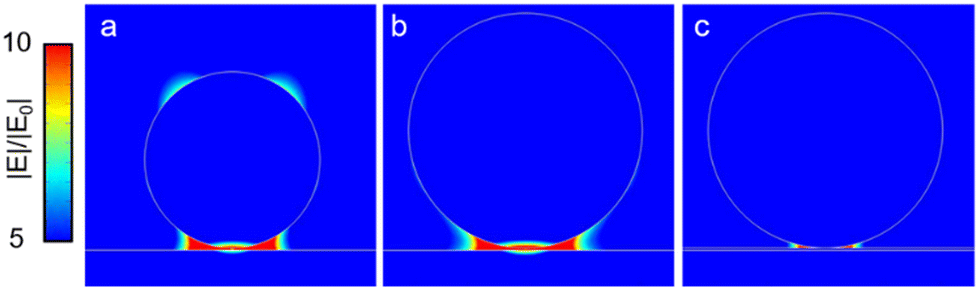 | ||
| Fig. 3 FEM simulations of a Rh nanoparticle deposited on an Al film. Excitation wavelength 266 nm (illumination from the top). Electromagnetic field enhancement factor. (a) Rh nanoparticle with a diameter of 150 nm; (b) Rh nanoparticle with a diameter of 200 nm; (c) Rh nanoparticle with a diameter of 200 nm on a film of Al considering an additional 2 nm Al2O3 layer in the gap. | ||
In order to facilitate the discussion of the experimental results before the assumption of a potential electromagnetic enhancement of SERS, we performed finite elements method (FEM) simulations using Comsol Multiphysics. Different experimental diameters of the obtained Rh NPs have been considered (150 and 200 nm in Fig. S3 – additional one in the ESI†) on top of a uniform Al layer.
Once the Rh NPs are illuminated with an external unpolarized light source at 260 nm, the obtained electromagnetic field intensities (Fig. 3) resemble the particle-on-mirror configuration.48 As can be observed in Fig. 3a and b, the field is mainly localized in the gap between the NPs and the metallic film underneath. Moreover, it is reasonable to assume that a thin oxide layer can form at the Al film surface; thus we also considered the presence of a 2 nm Al2O3 layer in the gap (Fig. 3c). In this case the field is even more confined in the gap between the continuous thin film and the RhNP. In our experiments, the adenine molecules were evaporated by means of sublimation directly on the surface of the RhNPs on the Al films. Being a directional process, it is reasonable to expect that the molecules were deposited on the upper surface of the NPs and on the Al surface not covered with the NPs, and so not in the direct vicinity of the highly confined and enhanced electric field. For this reason, we can expect that only very few molecules are present in the gap between the NPs and the Al metal below. This would lead to the lower SERS signals observed in the experiments, as the field around the NPs themselves, facing the direction from which evaporation occurs, is low or moderate. As a consequence, the particle-on-mirror geometry, responsible for electric field funnelling, reduces the active area that could otherwise contribute to SERS enhancement.
As illustrated in Fig. 3 the EM field enhancement of up to tenfold in the gap, in case it is accessible, would lead to a SERS enhancement.
Although the Raman signal decreased increasing the amount of RhNPs on the samples, it is interesting to explore how these substrates contribute to the UV photo-degradation on the biomolecules. In fact, one of the main challenges to the optical probing of organic compounds by excitation in the UV is their photo-degradation due to resonance with a multitude of electronic transitions. Fig. 3 shows the signal at 1330 cm−1 in 30 spectra of adenine collected consecutively over a time course of 15 minutes. The mode at 1330 cm−1 corresponds to a skeletal vibration of the pyrimidine ring41 and its intensity could therefore be indicative of the decomposition of the molecule. There is a decrease of the signals at 1330 cm−1 of the adenine samples over time for all samples. The decrease in intensity of this band could indicate dissociation of skeletal purine ring bonds, and/or a re-orientation of the molecule on the nanostructure. For the sample without nanoparticles, we observed a rapid exponential decay in the signal intensity at 1330 cm−1 (Fig. 4A), followed by a slower decrease of the signal that is present for all samples. This is probably due to the structure of the unmodified NPA that results in optical properties that can accelerate the photo-damage of the deposited analyte. For the samples containing RhNPs, the decay occurs at lower rate (Fig. 4B–F). From linear fits of the signal intensities, it can be inferred that the rate of decrease is reduced for samples with a higher content of RhNPs (Fig. 4B–F). We suggest that in this case, the presence of the RhNPs that may hinder access of a fraction of the molecules to the underlying NPA helps prevent the rapid initial photo-decomposition. For the future preparation of NPA containing RhNPs, the architecture proposed here must be further optimized to ensure better metal–molecule interactions.
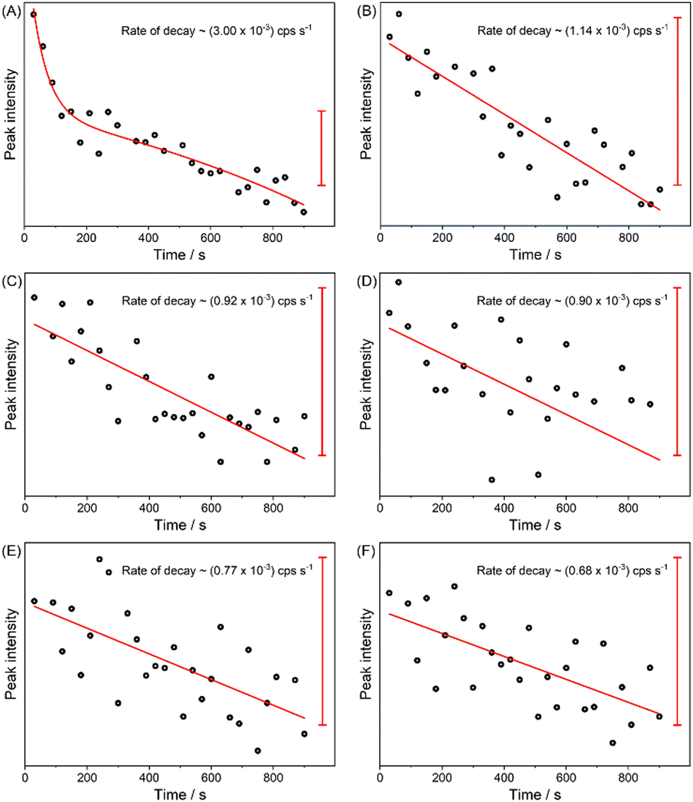 | ||
| Fig. 4 Signal intensities of the band at 1330 cm−1 for samples (A)–(F) defined in Table 1: (A) untreated porous Al; (B)–(F) samples of Rh-decorated porous Al. Scale bar corresponds to 1 count per second (cps). Acquisition time per spectrum: 300 s, excitation wavelength: 266 nm, excitation intensity: 0.8 W cm−2. | ||
Conclusions
In this paper a new, facile preparation procedure for a potential UV plasmonic platform was presented. The method relies on galvanic displacement reactions both for Al and Rh, two well-known metals with interesting plasmonic properties in the UV spectral range. The final samples look like a porous Al film covered with Rh NPs with a density of coverage that can be easily controlled by modifying the preparation parameters. The combination of a porous Al film with Rh NPs suggests applications in enhanced spectroscopies, in particular, in UV-SERS. By using a molecule excited at electronic resonance, adenine, we performed a large set of UV Raman experiments, first to check the enhancement produced by the platform depending on the density of Rh NPs on the material. An observed decrease in intensity of the Raman signals with the increasing Rh NP number suggests that the Rh NPs do not play a role in an enhancement of the adenine spectral signals. This, at first sight, could be counter-intuitive due to the observation of regions of high local fields in simulation results. Considering the actual geometry of the system, we suggest that the used biomolecule deposition method did not allow access of analyte molecules to the regions of high electromagnetic fields, leading us to explore other methods to place potential analyte molecules of interest in the gap between Rh NPs and the Al film.Analysis of the photostability of the organic molecule based on spectral signals confirms that Rh NPs reduce photodegradation, a property that could be beneficial in the future application of this optical material.
Experimental
Sample preparation
Square Al sheets 1 cm × 1 cm were cut from a commercial Al foil (99.99% Alfa Aesar, 1.5 mm thick). Polishing was performed using emery paper P1000 on both sides and then P4000 only on the side designated for the galvanic displacement (GD) process, until a homogeneous surface was achieved. At this stage the samples observed at SEM-EDS showed grooves due to mechanical scratching and inclusions of SiC particles. Al sheets were then submitted to ultrasonic treatment in water for 15 minutes to remove most residual SiC abrasive particles and dried. Prior to the GD process, Al sheets were etched in 5.0 M H2SO4 at 80 °C for 10 minutes, in order to eliminate residual SiC particles and obtain a more regular, renewed Al surface. Samples were then washed in water for 15 minutes with an ultrasonic bath and dried in a nitrogen flux (Fig. 1a). A polyester adhesive tape (3M 8992) was used to seal the back side, ensuring that GD processes occurred only on the front face.All GD processes were performed in solutions prepared from deionized water (by Elga-Veolia Purelab Pulse System ρ > 18 MΩ cm) and high-purity chemicals: NaCl (99.5% Merck), Na3RhCl6·12H2O (Alfa Aesar) and HCl (37% Merck). The solutions were aged for 48 h at 60 °C to ensure better reproducibility, due to the slow approach to equilibrium of the process of speciation of Rh chlorocomplexes.49,50
In preliminary trials the effect of pH was investigated. The use of pH 3 or higher caused slow Rh deposition and rather scattered results; pH 1 produced a rather fast reaction with the visible development of H2 gas bubbles and rapid Rh deposition, with some difficulty in controlling the extent of the latter. Optimal behaviour was observed at pH 2 and the reported data refer to this pH.
The series of samples considered in the following is reported in Table 1, where the experimental conditions of the GD treatment are given. The solutions – adjusted to pH 2 with HCl – were maintained at 25 °C, and deaerated with N2 for 20 minutes prior to sample immersion. Each sample is identified by a letter from (a) to (f) (Table 1). Most samples were prepared using a 0.5 mM Na3RhCl6 pH 2 solution, which offered the best conditions to control and standardise deposition. After the GD treatment, the samples were washed gently by immersion in ultrapure water, dried in a box saturated with N2, and stored under vacuum.
Scanning electron microscopy (SEM) images were obtained with a Zeiss SIGMA instrument, equipped using a field emission gun, operating under high vacuum conditions at an accelerating voltage of 20 kV. EDS analyses were performed at a 5 mm working distance with the same accelerating voltage reported above, using an Oxford X-MAX 20 mm2 apparatus, collecting data using software INCA 4.14 (Oxford Instruments). EDS atomic quantitative analyses were averaged over at least 3 areas at low magnification (×1000).
Atomic force microscopy (AFM)
AFM images were obtained in non-contact mode AFM using an AFM system XE-100.Total reflectance
Spectra were collected over the wavelength range of 200–2500 nm using an Agilent Cary5000 spectrophotometer with a 150 mm integration sphere.Sample functionalization with adenine
A thin layer of adenine was deposited on the substrates. The substrates were deposited with a thin layer of adenine in a thermal evaporator by sublimating solid adenine under 4.0 × 10⁻⁵ mbar. The film thickness was monitored in situ by a calibrated quartz crystal microbalance. The thickness of the final adenine layer was estimated to be about 2 nm.Raman spectroscopy
Raman experiments with excitation in the ultraviolet (UV) region were carried out at the Elettra Synchrotron radiation facility. A wavelength of 266 nm was used to probe the samples. The experimental setup consisted of a Czerny–Turner spectrograph of a collimator length of 750 mm, an entrance slit width of 100 μm, and a 1800 g mm−1 holographic grating that was coupled to a thermoelectrically cooled CCD detector. The spectral resolution was ∼8 cm−1 considering the full spectral range. Raman shift calibration was based on a spectrum of cyclohexane. From each sample, six spectra were collected consecutively with an acquisition time of 300 s per spectrum, yielding total respective collection times of 30 min per sample. The excitation intensity was adjusted to approximately 3.8 W cm−2 for this set of experiments. Another set of data, comprising 30 spectra was collected at a lower intensity of ∼0.8 W cm−2 from each sample, yielding total collection times of 15 min per sample.FEM simulations
Numerical simulations were carried out to investigate the optical response of the Rh nanoparticles on the Al substrate. The electromagnetic response of an isolated Rh nanoparticle was simulated using the finite-element method (FEM) implemented in Comsol Multiphysics®. The dimensions of the particles were set according to the average sizes obtained from the SEM images. The model computes electric field enhancement |E|/|E0| of the system. The unit cell was set to be 500 nm wide in both x- and y-directions and 1000 nm long in the z-direction, with perfect matching layers (200 nm thick) at the borders.Author contributions
SB, SW, QM, FDA, JK and YZ performed the Raman measurements and data analysis, LM and SC conceived and performed the film synthesis, NM and AS performed the numerical simulations, AD and GL provided support in sample preparation, RK provided support in data analysis and paper writing, and DG conceived the experiment and supervised the work. The authors thank Gabriele La Rosa for his support and the IIT clean room facility.Data availability
Data for this article, including all the SERS spectra are available at OFS.io at “Garoli, D. (2024, June 3). Porous aluminum decorated with rhodium nanoparticles. Retrieved from osf.io/zsvnw”.Conflicts of interest
There are no conflicts to declare.Acknowledgements
The authors thank the European Union under the Horizon 2020 Program, FET-Open: DNA-FAIRYLIGHTS, Grant Agreement 964995, the HORIZON-MSCA-DN-2022: DYNAMO, grant Agreement 101072818, and the Horizon Europe Program, Pathfinder Open: iSenseDNA, Grant Agreement 101046920. The authors thank the Clean Room Facility of IIT and Claudio Biagini for his technical support.Notes and references
- R. W. Wood, Philos. Mag., 1902, 4, 396–402 Search PubMed.
- M. I. Stockman, K. Kneipp, S. I. Bozhevolnyi, S. Saha, A. Dutta, J. Ndukaife, N. Kinsey, H. Reddy, U. Guler, V. M. Shalaev, A. Boltasseva, B. Gholipour, H. N. S. Krishnamoorthy, K. F. Macdonald, C. Soci, N. I. Zheludev, V. Savinov, R. Singh, P. Groß, C. Lienau, M. Vadai, M. L. Solomon, D. R. Barton, M. Lawrence, J. A. Dionne, S. V. Boriskina, R. Esteban, J. Aizpurua, X. Zhang, S. Yang, D. Wang, W. Wang, T. W. Odom, N. Accanto, P. M. D. Roque, I. M. Hancu, L. Piatkowski, N. F. V. Hulst and M. F. Kling, J. Opt., 2018, 20, 043001 Search PubMed.
- G. Barbillon, Materials, 2019, 12, 1502 Search PubMed.
- D. Gerard and S. K. Gray, J. Phys. D: Appl. Phys., 2015, 48, 184001 Search PubMed.
- J. M. McMahon, S. K. Gray and G. C. Schatz, Phys. Rev. B, 2010, 82, 035423 Search PubMed.
- T. Ding, D. O. Sigle, L. O. Herrmann, D. Wolverson and J. J. Baumberg, ACS Appl. Mater. Interfaces, 2014, 6, 17358–17363 Search PubMed.
- P. Ponzellini, G. Giovannini, S. Cattarin, R. P. Zaccaria, S. Marras, M. Prato, A. Schirato, F. D’Amico, E. Calandrini, F. De Angelis, W. Yang, H.-J. Jin, A. Alabastri and D. Garoli, J. Phys. Chem. C, 2019, 123, 20287–20296 Search PubMed.
- Y. Gutiérrez, R. Alcaraz de la Osa, D. Ortiz, Dolores, J. M. Saiz, F. González and F. Moreno, Appl. Sci., 2018, 8, 64 Search PubMed.
- H. O. Everitt, Y. Gutierrez, J. M. Sanz, J. M. Saiz, F. Moreno, F. Gonzalez and D. Ortiz, Opt. Express, 2016, 24, 20621 Search PubMed.
- A. Ahmadivand, R. Sinha, S. Kaya and N. Pala, Plasmonics, 2016, 11, 839–849 Search PubMed.
- K. Appusamy, X. Jiao, S. Blair, A. Nahata and S. Guruswamy, J. Phys. D: Appl. Phys., 2015, 48, 184009 Search PubMed.
- K. Watanabe, Y. Saito, M. Honda, Y. Kumamoto, S. Kawata and A. Taguchi, ACS Photonics, 2014, 1, 598–603 Search PubMed.
- M. W. Knight, N. S. King, L. Liu, H. O. Everitt, P. Nordlander and N. J. Halas, ACS Nano, 2014, 8, 834–840 Search PubMed.
- M. J. McClain, L. Zhou, S. Tian, O. Neumann, P. Nordlander, N. J. Halas, C. Zhang and X. Yang, Nano Lett., 2017, 17, 5071–5077 Search PubMed.
- J. Martin and J. Plain, J. Phys. D: Appl. Phys., 2015, 48, 184002 Search PubMed.
- Z. Ahmed, M. Agio, Y. Ekinci, J. F. Löffler and S. K. Jha, J. Am. Chem. Soc., 2012, 134, 1966–1969 Search PubMed.
- W. Yang, X.-G. Zheng, S.-G. Wang and H.-J. Jin, J. Electrochem. Soc., 2018, 165, C492–C496 Search PubMed.
- J. S. Corsi, J. Fu, Z. Wang, T. Lee, A. K. Ng and E. Detsi, ACS Sustainable Chem. Eng., 2019, 7, 11194–11204 Search PubMed.
- A. N. Koya, X. Zhu, N. Ohannesian, A. A. Yanik, A. Alabastri, R. P. Zaccaria, R. Krahne, W. Shih and D. Garoli, ACS Nano, 2021, 15, 6038–6060 Search PubMed.
- G. Ruffato, D. Garoli, S. Cattarin, S. Barison, M. Natali, P. Canton, A. Benedetti, D. D. Salvador and F. Romanato, Microporous Mesoporous Mater., 2012, 163, 153–159 Search PubMed.
- D. Garoli, E. Calandrini, G. Giovannini, A. Hubarevich, V. Caligiuri and F. D. Angelis, Nanoscale Horiz., 2019, 4, 1153–1157 Search PubMed.
- V. Caligiuri, H. Kwon, A. Griesi, Y. P. Ivanov, A. Schirato, A. Alabastri, M. Cuscunà, G. Balestra, A. De Luca, T. Tapani, H. Lin, N. Maccaferri, R. Krahne, G. Divitini, P. Fischer and D. Garoli, Nanophotonics, 2024, 13, 1159–1167 Search PubMed.
- D. Garoli, A. Schirato, G. Giovannini, S. Cattarin, P. Ponzellini, E. Calandrini, R. Proietti Zaccaria, F. D’Amico, M. Pachetti, W. Yang, H.-J. Jin, R. Krahne and A. Alabastri, Nanomaterials, 2020, 10, 102 Search PubMed.
- M. Tran, S. Roy, S. Kmiec, A. Whale, S. Martin, S. Sundararajan and S. Padalkar, Nanomaterials, 2020, 10, 644 Search PubMed.
- P. Vanysek, in 86th CRC Handbook of Chemistry and Physics, ed. D. R. Lide, 2006, pp. 8–20 Search PubMed.
- A. Ahmadivand, R. Sinha, S. Kaya and N. Pala, Plasmonics, 2016, 11, 839–849 Search PubMed.
- Y. Chen, Q.-S. Chen, S.-Y. Peng, Z.-Q. Wang, G. Lu and G.-C. Guo, Chem. Commun., 2014, 50, 1662–1664 Search PubMed.
- X. Zhang, P. Li, Á. Barreda, Y. Gutiérrez, F. González, F. Moreno, H. O. Everitt and J. Liu, Nanoscale Horiz., 2016, 1, 75–80 Search PubMed.
- P. Roy, S. Zhu, J.-B. Claude, J. Liu and J. Wenger, ACS Nano, 2023, 17, 22418–22429 Search PubMed.
- B. Nie, C. He and L. Liu, J. Raman Spectrosc., 2013, 44, 1512–1517 Search PubMed.
- C. E. Garoli, D. M. Ardini, J. A. Huang, C. Sanchez-Sanchez, P. Ponzellini, N. Maccaferri, A. Jacassi and S. Cattarin, in SPIE Conf. Proceeding, ed. T. Tanaka and D. P. Tsai, SPIE, 2017, p. 14.
- S. P. A. Fodor, R. P. Rava, T. R. Hays and T. G. Spiro, J. Am. Chem. Soc., 1985, 107, 1520–1529 Search PubMed.
- M. Pézolet, T. Yu and W. L. Peticolas, J. Raman Spectrosc., 1975, 3, 55–64 Search PubMed.
- W. L. Kubasek, B. Hudson and W. L. Peticolas, Proc. Natl. Acad. Sci. U. S. A., 1985, 82, 2369–2373 Search PubMed.
- V. Merk, E. Speiser, W. Werncke, N. Esser and J. Kneipp, Appl. Spectrosc., 2021, 75, 994–1002 Search PubMed.
- A. Y. Hirakawa, H. Okada, S. Sasagawa and M. Tsuboi, Spectrochim. Acta, Part A, 1985, 41, 209–216 Search PubMed.
- R. P. Lopes, R. Valero, J. Tomkinson, M. P. M. Marques and L. A. E. Batista De Carvalho, New J. Chem., 2013, 37, 2691 Search PubMed.
- L. Cui, D.-Y. Wu, A. Wang, B. Ren and Z.-Q. Tian, J. Phys. Chem. C, 2010, 114, 16588–16595 Search PubMed.
- A. M. Watson, X. Zhang, R. A. D. L. Osa, J. M. Sanz, F. González, F. Moreno, G. Finkelstein, J. Liu and H. O. Everitt, Nano Lett., 2015, 15, 1095–1100 Search PubMed.
- F. Madzharova, Z. Heiner, M. Gühlke and J. Kneipp, J. Phys. Chem. C, 2016, 120, 15415–15423 Search PubMed.
- B. Giese and D. McNaughton, J. Phys. Chem. B, 2002, 106, 101–112 Search PubMed.
- T. Dörfer, M. Schmitt and J. Popp, J. Raman Spectrosc., 2007, 38, 1379–1382 Search PubMed.
- B. Ren, X.-F. Lin, Z.-L. Yang, G.-K. Liu, R. F. Aroca, B.-W. Mao and Z.-Q. Tian, J. Am. Chem. Soc., 2003, 125, 9598–9599 Search PubMed.
- H. Zhang, X. Xia, W. Li, J. Zeng, Y. Dai, D. Yang and Y. Xia, Angew. Chem., Int. Ed., 2010, 49, 5296–5300 Search PubMed.
- K. B. Mogensen, M. Gühlke, J. Kneipp, S. Kadkhodazadeh, J. B. Wagner, M. Espina Palanco, H. Kneipp and K. Kneipp, Chem. Commun., 2014, 50, 3744–3746 Search PubMed.
- K. Karpiński, S. Zielińska-Raczyńska and D. Ziemkiewicz, Sensors, 2021, 21, 4096 Search PubMed.
- J. J. Baumberg, J. Aizpurua, M. H. Mikkelsen and D. R. Smith, Nat. Mater., 2019, 18, 668–678 Search PubMed.
- N. Maccaferri, G. Barbillon, A. N. Koya, G. Lu, G. P. Acuna and D. Garoli, Nanoscale Adv., 2021, 3, 633–642 Search PubMed.
- E. Verlato, S. Cattarin, N. Comisso, L. Mattarozzi, M. Musiani and L. Vázquez-Gómez, Electrocatalysis, 2013, 4, 203–211 Search PubMed.
- L. Mattarozzi, S. Cattarin, N. Comisso, M. Musiani, L. Vázquez-Gómez and E. Verlato, ChemElectroChem, 2023, 10, e202201122 Search PubMed.
Footnote |
| † Electronic supplementary information (ESI) available. See DOI: https://doi.org/10.1039/d4ma00203b |
| This journal is © The Royal Society of Chemistry 2024 |