 Open Access Article
A polarization tunable incident angle tolerant dielectric metasurface-based color filter†
Soikot
Sarkar
 ,
Dip
Sarker
 and
Ahmed
Zubair
 *
*
Department of Electrical and Electronic Engineering, Bangladesh University of Engineering and Technology, Dhaka 1205, Bangladesh. E-mail: ahmedzubair@eee.buet.ac.bd
First published on 22nd August 2024
Abstract
We designed and analyzed an ingenious Si–SiO2–Si dielectric metasurface to obtain structural colorization harnessing the contrast between the refractive indices of dielectrics. Though a few Si-based dielectric metasurfaces were reported, the performances of these metasurfaces were poor. We analyzed the optical properties of the dielectric metasurface employing the finite-difference time-domain (FDTD) technique. Electric field distributions revealed our proposed dielectric metasurface reflected light for a particular polarized light due to the strong light–matter interactions and the asymmetric nature of the structure. We adopted structural parameters by utilizing a parametric sweep method. Our proposed structure can tune a high color difference by varying polarization angles. We achieved a high color difference of ∼68 for the TE-polarized plane wave with negligible optical loss. Amazingly, our proposed dielectric metasurface structure exhibited a color difference of ∼20 for a high angular tolerance of 60°. Our proposed dielectric metasurface structure can benefit diverse applications such as hyperspectral imaging, color filtering, and anti-counterfeiting applications.
1 Introduction
Photonic devices comprising plasmonic materials and dielectrics are the key components and building blocks of color filters,1–4 antennas,5 waveguides,6,7 modulators,8 polarizers,9 absorbers10 and detectors11 for diverse applications, from producing sustainable energy to hyperspectral imaging.10,12–14 The interaction between abundant plasmons in plasmonic materials and the electric field of light causes the excitation of surface plasmon resonances, leading to strong optical responses in the visible and near-infrared wavelength regimes.15 However, these materials have several limitations, such as optical losses, high cost, complementary metal–oxide semiconductor incompatibility, and a lack of adaptivity post-fabrication. On the other hand, dielectric materials can play a vital role in assuaging these limitations and exhibit strong optical responses in the visible wavelength regime. Additionally, devices using dielectric materials provide unique optical properties, which are conducive to the design of structural colorization. Color filters are indispensable elements in diverse photonic applications, such as displays,16 image sensors,11 decorative solar panels,17 and light-emitting diodes.18 Conventional color filters utilize colorant pigments, which rely on light absorption to generate a desired color.19 Such light-absorbing characteristics of conventional color filters cause the resulting colors to have low efficiency. A novel color filter can be designed by harnessing the dielectric material's reflectance and plasmonic properties.Recently, structural coloration has attracted researchers’ interest. High-index dielectrics to obtain vivid coloration were adopted.1 Meanwhile, the the scattering of nanostructures relies on the refractive index of the structure. Various dielectrics, such as silicon (Si),1 silicon nitride (SiN),20 silicon nitride (Si3N4), lithium titanate (LTO),21 and hafnium oxide (HfO2),22 were reported to harness their high refractive index for designing structural color filters. Amidst them, Si is the most abundant and fabrication-friendly material to employ as a dielectric resonator for structural colorization. Previously, researchers studied several Si-based nanostructures, such as grating structures,1 ring structures,23 nanoparticles,24 nanopillars,25 spherical structures,26 nanodisks,27 and cross-structures,28 experimentally and numerically for structural colorization applications. Gao et al. studied a 1D grating structure of Si on a SiO2 substrate layer;1 however, the color difference was poor for the proposed structure. Lee et al.29 and Park et al.30 reported rectangular and nanodisk-shaped hydrogenated amorphous silicon metasurface structures to generate vivid colorization. However, the metasurface structure covered a small wavelength region of the visible range. Li et al. proposed a Si-based nanopillar structure where the operating wavelength was a limiting factor.25 Therefore, a huge scope exists for designing Si-based fabrication-friendly nanostructures with enhanced performance parameters for coloration. Our study will open the way for designing Si-based dielectric metasurfaces, which will benefit imaging,14 filtering,31 and anti-counterfeiting32 applications.
In this study, we proposed an ingenious Si–SiO2–Si grating metasurface and studied the optical characteristics of the dielectric metasurface employing the FDTD method. We adopted the structural parameters of the dielectric metasurface by utilizing the parametric sweep. The electric field profile revealed our proposed metasurface reflected light for a particular polarized light due to the strong light–matter interactions. We studied the impact of structural parameters of Si and SiO2 on color palettes for our proposed dielectric metasurface. In addition, we analyzed the chromaticity diagram of the metasurface and examined the vivid colorization of different images. Furthermore, the performance parameters, such as color difference and optical loss, were calculated for our proposed dielectric metasurface. We investigated the impact of polarization and incident angles on the reflectance spectra and color difference for our proposed dielectric metasurface structure. An extensive comparative performance analysis was conducted between our proposed dielectric metasurface and previously reported metasurfaces.
2 Structure design and methodology
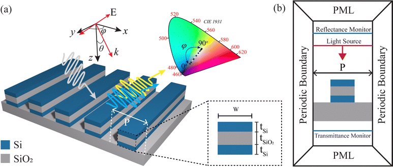
Si optoelectronics has the advantages of advanced fabrication techniques, facilities, and abundance; however, the optical performance of the planar Si structure is poor. Hence, various Si nanostructures comprising different materials were utilized for increased optical performance.10 Here, we designed an ingenious Si incorporated dielectric metasurface to harness the high refractive index and build a filtering mechanism of light in the visible wavelength. The interference between Si–air and Si–SiO2 provided a significant contrast in refractive index. Fig. 1(a) delineates the schematic illustration of our proposed Si–SiO2 dielectric metasurface. We used SiO2 as a spacer and substrate layer for our study to obtain low lattice mismatch and high efficiency. We adopted the complex refractive indices of Si and SiO2 from Palik33 (see Section S1 of the ESI† for details). The grating structure was prepared using vertically arranged subwavelength Si–SiO2–Si triple layers, where we considered air (na = 1) as the surrounding media in our study. This triple-layer grating structure offered improved results compared to the Si grating structure (see Section S2 of the ESI† for details). We discussed the suggested fabrication process in a later section. We define the duty cycle, f, of our proposed structure as | (1) |
Here, W and P denote the width and period of the grating. The W and P of the grating were set to be 100 and 260 nm. We adopted the thicknesses of Si, tSi and SiO2, tSiO2 to be 50 and 95 nm, respectively. All parameters were selected by conducting a parametric sweep in the Lumerical FDTD module (see Section S3 of the ESI† for details).
We performed the optical performance analysis of our proposed dielectric metasurface employing the two-dimensional (2D) FDTD technique (Ansys Lumerical). Our proposed grating dielectric metasurface structure was periodic in the x-direction and infinitely long in the y-direction; thus, we adopted a 2D FDTD numerical study to minimize the computational space and time. Moreover, we employed the periodic boundary condition in the x-direction with 12 perfectly matched layer (PML) boundary conditions in the z-direction so that the reflectance and transmittance lights from the simulation region were absorbed efficiently. The auto-shutoff level was set to be 10−5. A continuous wave (CW) plane wave with a wavelength of 380–780 nm was incident on the structure along the z-direction. We utilized transverse magnetic (TM) (φ = 0°) and transverse electric (TE) (φ = 90°)-polarized plane waves. Here, φ is the polarization angle.
Two frequency-domain fields and power monitors were positioned at the top of the light source and beneath the proposed structure to enumerate the reflectance, R(λ), and transmittance, T(λ). The simulation setup is illustrated in Fig. 1(b). R(λ) and T(λ) were calculate as follows:
 | (2) |
 | (3) |
| A(λ) = 1 − R(λ) − T(λ). | (4) |
Here, PR(λ), PT(λ), and PI(λ) are the reflected, transmitted, and incident power, respectively. The temperature of the simulation environment was set to be 300 K. We created a benchmark of our simulation compared with the previously reported experimental and numerical works (see Section S4 of the ESI† for details). Additionally, we investigated the chromaticity chart using the CIE (Commission Internationale de l’Éclairage) 1931 diagram to estimate the reflected color from our proposed dielectric metasurface structure. Here, we employed the CIE DE2000 color difference formulas to evaluate the color difference.
3 Results and discussion
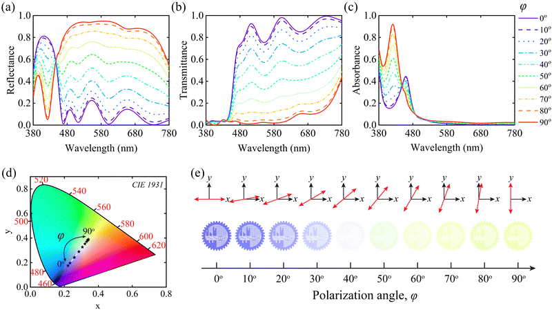
Our proposed dielectric metasurface structure, which worked as a color filter in reflection geometry, had polarization tunability, as shown in Fig. 2. Fig. 2(a)–(c) illustrate the reflectance, transmittance, and absorbance spectra of the proposed color filter within the visible wavelengths (380–780 nm) of light. To determine the polarization angle dependency of the filter, these parameters were computed using a light source with polarization angles (φ) ranging from 0° to 90°, where a difference of 10° was considered between any two successive polarization angles.The reflectance or transmittance of any linearly polarized light can be characterized as the combination of the reflectance of transmittance for two polarizations that are perpendicular to each other. Therefore, the reflectance and transmittance for any polarization angle for this device can be expressed as follows:1,34
| Rφ(λ) = R0°(λ)cos2φ + R90°(λ)sin2φ | (5) |
| Tφ(λ) = T0°(λ)cos2φ + T90°(λ)sin2φ. | (6) |
R
0° and T0° represent the reflectance and transmittance at φ = 0°. R90° and T90° depict the reflectance and transmittance for the light with φ = 90°. We theoretically calculated the reflectance spectrum by utilizing eqn (5) for φ = 40°, exhibiting the same result, obtained from numerical analysis (see Section S5 of the ESI†). We considered the reflectance of incident light at various polarization angles to create a wide range of colors. Fig. 2(a) illustrates that there was a shift towards longer wavelengths (redshift) in the peak of the reflectance spectra when the φ was changed from 0° to 90°. Moreover, a broader effect of the reflectance spectra was noted. These characteristics of the reflectance spectra can be easily understood by the electric field distribution and will be addressed in subsequent discussions. A wide bandwidth peak in the reflectance spectra was obtained due to the addition of multiple electric modes, as our proposed metasurface structure exhibited domination for the electric fields, as shown in Fig. 3. The chromaticity coordinates were determined using these reflectance spectra corresponding to various φ. Subsequently, the chromaticity coordinates were plotted on the CIE 1931 chromaticity diagram, which provides quantitative relationships between wavelength distributions in the electromagnetic visible spectrum and physiologically experienced colors in human color vision, as depicted in Fig. 2(d). This chromaticity diagram displays a smooth gradient of colors ranging from blue to yellow, corresponding to φ from 0° to 90°. These generated reflected colors are illustrated in Fig. 2(e) as the logo color of Bangladesh University of Engineering and Technology (BUET). The spectra can be transformed into three standard tristimulus values X, Y, and Z by adopting the standard color-matching functions ![[x with combining macron]](https://www.rsc.org/images/entities/i_char_0078_0304.gif) , ȳ, and
, ȳ, and ![[z with combining macron]](https://www.rsc.org/images/entities/i_char_007a_0304.gif) of the standard observers. The tristimulus values X, Y, and Z can be calculated by using the following equations:
of the standard observers. The tristimulus values X, Y, and Z can be calculated by using the following equations:
 | (7) |
 | (8) |
 | (9) |
Here, E and R represent the radiation of the light source and reflection coefficient, respectively. The chromaticity coordinates of the CIE diagram can be determined from the tristimulus values using the following equations:
 | (10) |
 | (11) |
 | (12) |
For the 2D CIE 1931 chromaticity diagram, the x and y are relatively red and green coordinates whereas the z is unnecessary.
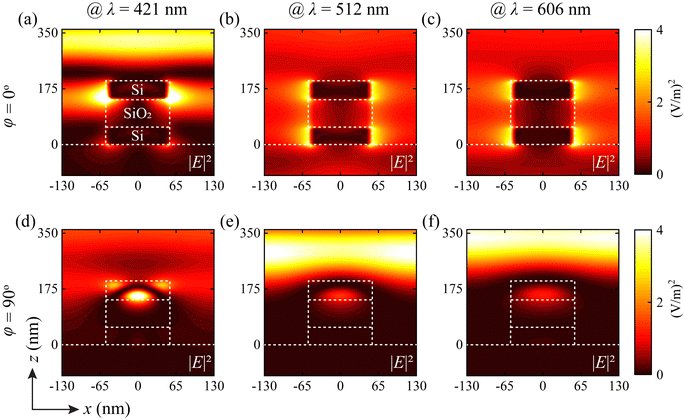
The electric field (|E|2) distributions of our proposed structure in the xz plane are illustrated in Fig. 3(a)–(c) for φ = 0° and in Fig. 3(d)–(f) for φ = 90°, where we considered the wavelengths of 421 nm, 512 nm, and 606 nm. At the wavelength of 421 nm, it is obvious that a significant amount of incident light was reflected, and a smaller amount was absorbed by the Si and SiO2 layer for φ = 0°. Meanwhile, a significant absorption was observed at the first interface of Si and SiO2 when φ was set to 90°. In contrast, the second interface absorbed a minimal amount of light due to the lack of transmitted light from the first interface (see Section S6 of the ESI† for details). For the wavelengths of 512 nm and 606 nm, enormous amounts of transmission and reflection were observed for φ = 0° and φ = 90° respectively. The aforementioned characteristics of reflectance, transmittance, and absorbance of Fig. 2(a)–(c) can be easily comprehended from the electric field (|E|2) distributions.
3.1 Effect of the thickness of the Si layer
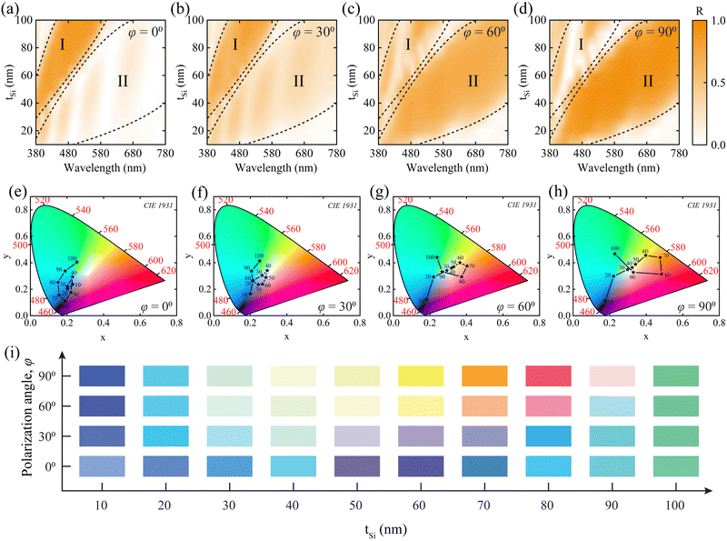
The characteristics of our proposed polarization tunable color filter were analyzed by changing the thickness of the Si layer. The tSi was varied from 10 to 100 nm with a difference of 10 nm between two successive thicknesses, while the thickness of the SiO2 layer, tSiO2 = 95 nm, was kept constant. Moreover, to maintain a uniform duty cycle, the width of the grating layer, W, was also kept constant. The reflectance spectra for both polarization φ = 0° and φ = 90° are illustrated in Fig. 4. A redshift of resonance wavelength of the reflectance spectra was observed with the change of tSi for both polarization angles. This characteristic can be more rigorously understandable from Fig. 5(a)–(d) where the reflectance spectra are illustrated for four different φ of 0°, 30°, 60°, and 90°. A redshift and the broadening phenomena of the reflectance spectra were observed with the change of tSi. The combination of these two phenomena generated an extensive spectrum of color variations, as illustrated in Fig. 5(e)–(h).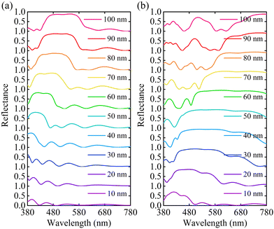 | ||
| Fig. 4 Reflectance spectra of the dielectric metasurface structure for different tSi values at (a) φ = 0° and (b) φ = 90°. Other structural parameters were kept constant. | ||
These CIE chromaticity diagrams corresponding to different polarization angles were determined from the reflectance spectra. The asterisk sign denotes the chromaticity coordinates for different tSi values. To analyze the chromaticity coordinates for various φ values, we divided the reflectance spectra into two separate regions: I and II. According to the findings shown in Fig. 5(a)–(d), it is obvious that the intensity of region I reduced when the φ was rotated from 0° to 90°. In contrast, an increase in the intensity of region II was noted. Moreover, the red shift and broadening effect phenomena were observed for regions I and II. Consequently, some of the chromaticity coordinates experienced a shift from the bluish to reddish and yellowish region when the polarization angle was rotated. Fig. 5(i) depicts a 2D array of colors that demonstrates how the color changes with variations in the tSi as well as the φ. The colors were picked from the CIE chromaticity diagram based on their appropriate φ. When the φ was rotated, a pronounced color shift was seen throughout the Si layer thickness range of 20 nm to 90 nm. The variation in color with the φ was somewhat lower for Si layers with thicknesses, tSi, of 10 nm and 100 nm compared to the others. To evaluate the color differences due to the change in the φ, we considered the CIE DE2000 formula.35 The color difference between two sets  , and
, and  in the CIELAB space can be determined using the following equations (see Section S7 of the ESI† for details):35
 | (13) |
The color difference corresponds to the 2D array of Fig. 5(i) listed in Table 1. We have found a color difference of 68.04 for our proposed dielectric metasurface when the φ was rotated from 0° to 90°. A maximum color difference of 88.92 was found for the Si layer thickness of 80 nm. As we mentioned the color variation for tSi of 10 and 100 nm was lower which can be rigorously observed from this table. Color differences of 15.06 and 15.27 were found for the tSi of 10 and 100 nm, respectively.
| t Si (nm) | ||||||||||
|---|---|---|---|---|---|---|---|---|---|---|
| 10 | 20 | 30 | 40 | 50 | 60 | 70 | 80 | 90 | 100 | |
| φ = 0° | 0 | 0 | 0 | 0 | 0 | 0 | 0 | 0 | 0 | 0 |
| φ = 30° | 7.07 | 21.70 | 25.37 | 24.20 | 25.11 | 24.90 | 18.97 | 11.82 | 5.11 | 2.93 |
| φ = 60° | 12.91 | 45.49 | 46.95 | 43.24 | 59.74 | 71.50 | 49.98 | 77.44 | 21.27 | 10.34 |
| φ = 90° | 15.06 | 50.91 | 52.70 | 48.52 | 68.04 | 85.50 | 62.72 | 88.92 | 42.08 | 15.27 |
A reference maple leaf and a 2D array of maple leaves are illustrated in Fig. 6(a) and (b), respectively.
The color of each leaf was determined by multiplying the reflected color from the structure with the color of the reference maple leaf. The reflected colors were taken from the two-dimensional color array depicted in Fig. 5(i). A wide range of color variations, including shades of green, red, yellow, black, and brown, were observed in maple leaves in terms of the reference color of the leaf.
3.2 Effect of the grating width
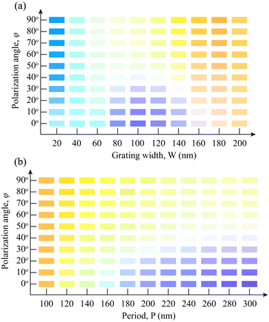
The proposed reflective color filter was a one-dimensional periodic dielectric grating structure that was composed of a stack of Si–SiO2–Si layers. We investigated the performance of our proposed dielectric grating-based metasurface by changing the width of the grating layers, W, as well as the polarization angle, φ. We considered a wide range of W from 20 nm to 200 nm in this regard. However, the length of the period, P, was kept constant at 260 nm. The φ was incrementally rotated from 0° to 90° with a step of 10° for each width of the grating layers. Fig. 7(a) illustrates a two-dimensional array of colors, with the horizontal axis representing the width of the grating layers and the vertical axis representing the polarization angle. The colors were picked from the corresponding CIE chromaticity diagram. The polarization angle tunability characteristic was observed for W ranging from 80 nm to 160 nm, resulting in a continuous color palette ranging from blue to yellow. In contrast, this polarization angle tunability characteristic was not found for the other grating widths. Our proposed structure with 100 nm provided a continuous color palette, though a little change (∼±10 nm) in grating width would not significantly impact its performance, implying the fabrication of the proposed color filter is feasible (see Section S8 of the ESI†).3.3 Effect of periodicity
As our proposed color filter was periodic in one dimension (x-direction), the periodicity of this structure was an important factor to consider in achieving the required performance. A study was conducted to explore the color filtering performance by varying the periodicity of our dielectric grating structure, P, as well as the polarization angle, φ. In this regard, we have considered a constant width of the grating layers, W. Since the W was 100 nm, we varied the P from 100 to 300 nm with an increment of 20 nm. We explored the characteristics of the polarization angle tunability for each period length by systematically varying the φ from 0° to 90° with a step size of 10°. Fig. 7(b) depicts a 2D array of colors, where the horizontal axis represents P and the vertical axis represents φ. The colors were selected from the corresponding CIE chromaticity diagram. The absence of polarization tunability was observed at P values of 100 nm and 120 nm when the φ was rotated. The polarization tunability characteristic was exhibited by the structure from the P of 140 nm. However, the range of color was found to be lower for P values of 140 nm and 160 nm. Within the periodicity range of 180 nm to 300 nm, a continuous palette of color ranging from blue to yellow was observed with the change of the φ.3.4 Effect of the incidence angle
The property of incidence angle tolerability of our proposed dielectric metasurface can be explained by the relative resonance wavelength shifting of reflectance spectra. Let λo be the resonance wavelength under normal incidence and Δλ represent the shift in resonance wavelength caused by oblique incidence. In this case, we can define the relative shift in resonance wavelength as follows: | (14) |
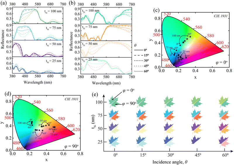
Here, we investigated the impact of the incidence angle, θ, ranging from 0° to 60° with an increment of 15° for different thicknesses of the Si layer, tSi, of our proposed dielectric grating metasurface. We conducted this investigation for φ values of 0° and 90°. Fig. 8(a) and (b) illustrate the reflectance spectra for different tSi with varying θ for the φ values of 0° and 90°, respectively. In this case, we considered the tSi ranging from 25 nm to 100 nm with an increment of 25 nm. For the φ of 0°, we found the maximum relative resonance wavelength shifting of 10% for the 75 nm of Si layer thickness at the θ of 60°. However, the reflectance spectra exhibited a high degree of similarity when the incidence angles were varied for a specific thickness of the Si layer. As a result, we found that the colors produced by these reflections of the proposed color filter were quite similar. The corresponding chromaticity coordinates were calculated by these reflectance spectra and plotted in the CIE diagram, illustrated in Fig. 8(c). The chromaticity coordinates are denoted by the asterisk sign, whereas the arrow sign indicates the shift of the chromaticity coordinates with the θ for different tSi. From this CIE diagram, it is obvious that the variation of the color with the change of θ is negligible for all the dielectric grating structures based on different tSi. An obvious understanding regarding this can be obtained from Table 2, where the color differences were calculated using the CIE DE2000 formula. When the φ was 0°, the maximum color difference was 26.33 at a θ of 60° for 75 nm of tSi.
| φ = 0° | φ = 90° | |||||||
|---|---|---|---|---|---|---|---|---|
| t Si (nm) | 25 | 50 | 75 | 100 | 25 | 50 | 75 | 100 |
| θ = 0° | 0 | 0 | 0 | 0 | 0 | 0 | 0 | 0 |
| θ = 15° | 2.69 | 2.27 | 1.59 | 1.58 | 2.14 | 2.04 | 0.61 | 0.73 |
| θ = 30° | 9.57 | 8.13 | 6.21 | 5.94 | 9.03 | 7.71 | 1.95 | 2.46 |
| θ = 45° | 17.42 | 14.87 | 13.71 | 11.96 | 27.42 | 15.15 | 2.53 | 3.99 |
| θ = 60° | 20.48 | 17.83 | 26.33 | 18.22 | 42.49 | 21.65 | 2.04 | 5.66 |
For the φ of 90° and the tSi of 25 nm, the reflectance spectra exhibited a fluctuation when the angle of the incidence was varied. In this case, we found the relative resonance wavelength shifting of 18.24% and 19.19% for the θ of 45° and 60°, respectively. Moreover, the shape of the reflectance spectra was not similar for these angles of incidence. Moreover, the electric field distribution corroborated this phenomenon (see Section S9 of the ESI† for details). As a result, for the grating structure with 25 nm of tSi, a notable fluctuation of color was observed in the CIE chromaticity diagram, illustrated in Fig. 8(d). Moreover, this phenomenon can be observed in Table 2 where significant color differences were observed for 25 nm of tSi at the incidence angle, θ, of 45° and 60° which were 27.42 and 42.49, respectively. However, for other grating structures with tSi values of 50 nm, 75 nm, and 100 nm, the reflectance spectra exhibited the same patterns when θ was varied. As a result, negligible variations of the color with different incidence angles were observed, which are presented in Fig. 8(d) and Table 2. Fig. 8(e) illustrates a 2D array of maple leaves where the maple leaves are divided into two halves. The left and right half of the maple leaf represent the color for φ values of 0° and 90°, respectively, with varying θ and tSi. The x- and y-axes indicate the incidence angle and the thickness of the Si layer, respectively. The colors of these maple leaves were picked from the CIE chromaticity diagram of Fig. 8(c) and (d). This 2D array also clearly interprets the phenomenon we mentioned earlier. All grating structures have shown remarkable performance for oblique incidence of light source except for the grating structure with a tSi of 25 nm for a φ of 90° and a tSi of 75 nm for a φ of 0°.
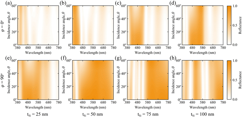
The reflectance spectra for different incidence angles mentioned earlier can be more understandable from Fig. 9. Here, Fig. 9(a)–(d) and (e)–(h) illustrate the reflectance spectra with varying θ as well as tSi values of our proposed grating structure for φ values of 0° and 90°, respectively. In this case, tSi increases from 25 to 100 nm, and the θ increases from 0° to 60°. It is obvious that, with the change in the θ, the valleys of the reflectance were similar. However, the intensity of these reflectance spectra exhibited decreasing phenomena when the θ was increased above 45°. Moreover, the slight shifting of the resonance wavelength was also observed from these reflectance spectra. Hence, a fluctuation of color was observed when the θ was varied.
3.5 Optical loss
We considered the reflectance of our proposed dielectric grating structure for producing a color palette with changing polarization angles. In contrast, we adopted the transmittance and absorptance to be optical loss. We calculated the optical loss asLoss = −10![[thin space (1/6-em)]](https://www.rsc.org/images/entities/char_2009.gif) log10(PR(λ)). log10(PR(λ)). | (15) |
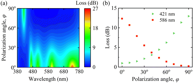
Here, PR(λ) denotes the reflected power. Fig. 10(a) illustrates the optical loss of our proposed dielectric metasurface structure when we varied the φ from 0° to 90°. The FWHM and resonance wavelength broadened and redshifted, respectively, when we increased the φ from 0° to 90°, as shown in Fig. 2(a). Thus, we observed the optical loss at the shorter wavelength when the φ was around 90°. We found the optical loss at the higher wavelength of incidence light for the φ around 0°. This characteristic exhibited the opposite pattern of the reflectance spectrum. Here, we have found the maximum optical loss of 25.68 dB at the wavelength of 733 nm for the φ of 0°. Fig. 10(b) depicts the optical loss at 421 and 586 nm resonance wavelengths for varying φ. The resonance wavelength was redshifted while we varied the φ from 0° to 90°. Hence, the optical loss at 421 nm became higher, whereas the optical loss was lower at the wavelength of 586 nm with rotating the φ from 0° to 90°. We measured the maximum optical loss of 12.95 and 12.32 dB for 421 and 586 nm wavelengths, respectively.
4 Comparative analysis
Table 3 demonstrates an extensive comparative study of performance parameters between our proposed dielectric grating metasurface and previously reported structures. Gao et al. reported a reflective color filter with an operating wavelength range of 380 nm to 780 nm wherein the proposed structure was designed to harness a 1D Si grating.1 The structure exhibited a maximum color difference of 55.32, operating an oblique incidence range from 0° to 60°. Moreover, they reported a transmissive type 1D dielectric–metal–dielectric grating filter with an operating wavelength range of 400 to 700 nm.36 Ellenbogen et al. introduced a transmissive color filter designed with an asymmetrical metal-cross structure.37 Their structure operated in a wavelength range from 460 to 620 nm. Yang et al. introduced a reflective MIM square grating structure, operated at the wavelength range of 380 to 780 nm.38 Koirala et al.,4 Park et al.,31 and Yang et al.31,39 reported all-dielectric color filters by utilizing TiO2, Si-rich SiN, and Si nanopillars, respectively. The tunability of these structures was achieved by varying the structural parameters, especially the diameter of nanopillars, in a limited wavelength region. Thus, multiple structures are required to tune the color. On the other hand, our proposed 1D Si–SiO2 dielectric grating reflective metasurface was operated in the visible wavelength region with a range of 380 to 780 nm; thus, the colorization can be tuned by varying the polarization angle. Our proposed structure exhibited remarkable performance when we operated it at an oblique incidence angle of the light range of 0° to 60°. The maximum color difference was calculated to be 42.49 at the incidence angle of 60° when the thickness of the Si layer and the polarization angle were set to be 25 nm and 90°, respectively.| Structure type | Filter type | Wavelength range (nm) | Operating incidence angle range (°) | Color differences for oblique incidence (max) | Ref. |
|---|---|---|---|---|---|
| 1D silicon grating | Reflective | 380–780 | 0–60 | 55.32 | 1 |
| 1D dielectric–metal–dielectric grating | Transmissive | 400–700 | — | — | 36 |
| Asymmetrical metal-cross structure | Transmissive | 460–620 | — | — | 37 |
| MIM square grating | Reflective | 380–780 | — | — | 38 |
| Cylindrical TiO2 nanopillars with different diameters | Transmissive | 400–800 | 0–25 | — | 4 |
| Si-rich SiN nanodisk | Transmissive and reflective | 400–800 | — | — | 31 |
| Si nanopillars with an RI matching layer | Reflective | 375–700 | — | — | 39 |
| 1D Si–SiO2 dielectric grating | Reflective | 380–780 | 0–60 | 42.49 | This work |
5 Suggested fabrication technique
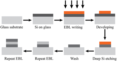
Previously, researchers created Si–SiO2 grating structures by employing electron beam lithography (EBL).40–42 The suggested fabrication process can be adopted to achieve our Si–SiO2–Si grating dielectric metasurface. The suggested fabrication process is shown in Fig. 11. There was negligible lattice mismatch due to the good adhesiveness of Si and SiO2. We adopted SiO2 as a substrate layer for our structure, and Si can be grown on the substrate layer by using the deposition technique. Then, the EBL writing and development provided a photoresist mask on the structure where light would not penetrate. The laser etched the Si layer except for the photoresist mask region. After that, the photoresist layer was removed by a solvent. In general, acetone and NMP (1-methyl-2-pyrrolidone) are used as suitable solvents for removing photoresist layers; however, academicians avoid acetone due to its high vapor pressure. The Si grating on the SiO2 substrate was produced after removing the photoresist layer. The Si–SiO2–Si grating dielectric metasurface may be produced after repeating the EBL technique twice.6 Conclusions
We proposed a polarization-tunable ingenious one-dimensional Si–SiO2–Si dielectric metasurface and analyzed its optical properties employing the FDTD method. Specifically, we utilized the high refractive index contrast between Si and SiO2 dielectrics to obtain vivid structural colorization. Our proposed dielectric metasurface structure not only exhibited continuous color palettes by altering the polarization angles but also produced vivid structural colorization by adjusting structural parameters. A high color difference from 0 to ∼68 was obtained by changing φ from 0° to 90° for tSi = 50 nm. The color difference can be increased by increasing the tSi. In contrast, our proposed dielectric metasurface structure exhibited a color difference of ∼20 for a high angular tolerance of 60° for both TM and TE polarization plane waves. Additionally, our proposed structure showed a minuscule loss of ∼0 dB at 421 and 586 nm wavelengths for TM- and TE-polarized lights, respectively, which ensured high-grade vivid colors through the reflection mechanism. According to our extensive comparative study, our proposed dielectric structure outperformed previously reported Si-based metasurface structures. Furthermore, a suggested fabrication technique demonstrated the dielectric grating metasurface is feasible to fabricate. Our study will pave the way to designing Si-based dielectric metasurface structures, which will be beneficial for imaging, filtering, and anti-counterfeiting applications.Author contributions
Soikot Sarkar: conceptualization, methodology, visualization, software, investigation, writing – original draft, and writing – review & editing. Dip Sarker: conceptualization, methodology, visualization, software, investigation, writing – original draft, and writing – review & editing. Ahmed Zubair: conceptualization, methodology, visualization, resources, supervision, writing – original draft, and writing – review & editing.Data availability
The code and simulation file for this article are available at GitHub at https://github.com/ahmedzubair003/colorfilter.git.Conflicts of interest
The authors declare no conflict of interest.Acknowledgements
S. Sarkar, D. Sarker, and A. Zubair thank the Department of Electrical and Electronic Engineering, Bangladesh University of Engineering and Technology (BUET) for providing the Ansys Lumerical software and the necessary support. D. Sarker acknowledges the financial support from BUET through its Postgraduate Fellowship program.References
- X. Gao, Q. Wang, N. Luo, B. Xu, R. Hong, D. Zhang and S. Zhuang, Opt. Express, 2021, 29, 41246–41257 CrossRef CAS.
- I. Kim, J. Jang, G. Kim, J. Lee, T. Badloe, J. Mun and J. Rho, Nat. Commun., 2021, 12, 3614 CrossRef CAS PubMed.
- J. Jang, T. Badloe, Y. Yang, T. Lee, J. Mun and J. Rho, ACS Nano, 2020, 14, 15317–15326 CrossRef CAS PubMed.
- I. Koirala, S.-S. Lee and D.-Y. Choi, Opt. Express, 2018, 26, 18320–18330 CrossRef CAS PubMed.
- M. Hrtoň, A. Konečná, M. Horák, T. c v Šikola and V. Křápek, Phys. Rev. Appl, 2020, 13, 054045 CrossRef.
- X. Qin, W. Sun, Z. Zhou, P. Fu, H. Li and Y. Li, Nanophotonics, 2022, 11, 1659–1676 CrossRef CAS.
- Y. Meng, Y. Chen, L. Lu, Y. Ding, A. Cusano, J. A. Fan, Q. Hu, K. Wang, Z. Xie, Z. Liu, Y. Yang, Q. Liu, M. Gong, Q. Xiao, S. Sun, M. Zhang, X. Yuan and X. Ni, Light: Sci. Appl., 2021, 10, 235 CrossRef CAS.
- D. Sarker, P. P. Nakti and A. Zubair, Opt. Express, 2024, 32, 9442–9455 CrossRef CAS.
- D. Sarker, P. P. Nakti, M. I. Tahmid, M. A. Z. Mamun and A. Zubair, Opt. Express, 2021, 29, 42713–42725 CrossRef CAS.
- P. P. Nakti, D. Sarker, M. I. Tahmid and A. Zubair, Nanoscale Adv., 2023, 5, 6858–6869 RSC.
- A. Rawat, A. Ahamed, C. Bartolo-Perez, A. S. Mayet, L. N. McPhillips and M. S. Islam, ACS Photonics, 2023, 10, 1416–1423 CrossRef CAS PubMed.
- W. Zhang, J. C. Lederman, T. Ferreira de Lima, J. Zhang, S. Bilodeau, L. Hudson, A. Tait, B. J. Shastri and P. R. Prucnal, Light: Sci. Appl., 2024, 13, 14 CrossRef CAS PubMed.
- B. Yao, S.-W. Huang, Y. Liu, A. K. Vinod, C. Choi, M. Hoff, Y. Li, M. Yu, Z. Feng, D.-L. Kwong, Y. Huang, Y. Rao, X. Duan and C. W. Wong, Nature, 2018, 558, 410–414 CrossRef CAS PubMed.
- I. Kim, H. Kim, S. Han, J. Kim, Y. Kim, S. Eom, A. Barulin, I. Choi, J. Rho and L. P. Lee, Adv. Mater., 2023, 35, 2300229 CrossRef CAS PubMed.
- D. Sarker and A. Zubair, Phys. Chem. Chem. Phys., 2024, 26, 10273–10283 RSC.
- Y. J. Liu, G. Y. Si, E. S. P. Leong, N. Xiang, A. J. Danner and J. H. Teng, Adv. Mater., 2012, 24, OP131–OP135 CAS.
- C. Ji, Z. Zhang, T. Masuda, Y. Kudo and L. J. Guo, Nanoscale Horiz., 2019, 4, 874–880 RSC.
- X. Peng, Y. Zeng, S. Huo, Z. Yang, X. Huang and Q. Zhao, Photonic Sens., 2023, 14, 240123 CrossRef.
- K.-T. Lee, S. Y. Han, Z. Li, H. W. Baac and H. J. Park, Sci. Rep., 2019, 9, 14917 CrossRef PubMed.
- C.-S. Park, I. Koirala, S. Gao, V. R. Shrestha, S.-S. Lee and D.-Y. Choi, Opt. Express, 2019, 27, 667–679 CrossRef CAS PubMed.
- C. Lipp, A. Jacquillat, D. Migliozzi, H.-C. Wang, A. Bertsch, E. Glushkov, O. J. Martin and P. Renaud, ACS Appl. Mater. Interfaces, 2023, 15, 33056–33064 CrossRef CAS PubMed.
- Y. Zhao, Z. Li, X. Liu, K. Wang, Y. Sun, H. Yang, X. Wang, T. Wang, N. Song and J. Gao, Opt. Express, 2022, 30, 22820–22829 CrossRef CAS PubMed.
- M. A. van de Haar, J. van de Groep, B. J. Brenny and A. Polman, Opt. Express, 2016, 24, 2047–2064 CrossRef CAS PubMed.
- Y. H. Fu, A. I. Kuznetsov, A. E. Miroshnichenko, Y. F. Yu and B. Luk’yanchuk, Nat. Commun., 2013, 4, 1527 CrossRef PubMed.
- L. Li, J. Niu, X. Shang, S. Chen, C. Lu, Y. Zhang and L. Shi, ACS Appl. Mater. Interfaces, 2021, 13, 4364–4373 CrossRef CAS PubMed.
- B. S. Luk’yanchuk, N. V. Voshchinnikov, R. Paniagua-Domínguez and A. I. Kuznetsov, ACS Photonics, 2015, 2, 993–999 CrossRef.
- A. I. Kuznetsov, A. E. Miroshnichenko, M. L. Brongersma, Y. S. Kivshar and B. Lukyanchuk, Science, 2016, 354, aag2472 CrossRef.
- V. Vashistha, G. Vaidya, R. S. Hegde, A. E. Serebryannikov, N. Bonod and M. Krawczyk, ACS Photonics, 2017, 4, 1076–1082 CrossRef CAS.
- T. Lee, J. Kim, I. Koirala, Y. Yang, T. Badloe, J. Jang and J. Rho, ACS Appl. Mater. Interfaces, 2021, 13, 26299–26307 CrossRef CAS PubMed.
- C.-S. Park, V. R. Shrestha, W. Yue, S. Gao, S.-S. Lee, E.-S. Kim and D.-Y. Choi, Sci. Rep., 2017, 7, 2556 CrossRef PubMed.
- C.-S. Park, I. Koirala, S. Gao, V. R. Shrestha, S.-S. Lee and D.-Y. Choi, Opt. Express, 2019, 27, 667–679 CrossRef CAS PubMed.
- Z. Xu, H. Luo, H. Zhu, Y. Hong, W. Shen, J. Ding, S. Kaur, P. Ghosh, M. Qiu and Q. Li, Nano Lett., 2021, 21, 5269–5276 CrossRef CAS PubMed.
- E. D. Palik, Handbook of Optical Constants of Solids, Elsevier Science, 1998 Search PubMed.
- I. Koirala, V. R. Shrestha, C.-S. Park, S. Gao, S.-S. Lee and D.-Y. Choi, Sci. Rep., 2017, 7, 13574 CrossRef PubMed.
- G. Sharma, W. Wu and E. N. Dalal, Color Res. Appl., 2005, 30, 21–30 CrossRef.
- X. Gao, Q. Wang, S. Cao, R. Li, R. Hong and D. Zhang, Opt. Express, 2020, 28, 25073–25084 CrossRef CAS PubMed.
- T. Ellenbogen, K. Seo and K. B. Crozier, Nano Lett., 2012, 12, 1026–1031 CrossRef CAS PubMed.
- C. Yang, W. Shen, Y. Zhang, H. Peng, X. Zhang and X. Liu, Opt. Express, 2014, 22, 11384–11391 CrossRef PubMed.
- W. Yang, S. Xiao, Q. Song, Y. Liu, Y. Wu, S. Wang, J. Yu, J. Han and D.-P. Tsai, Nat. Commun., 2020, 11, 1864 CrossRef CAS PubMed.
- Y. Zheng, X. Kai, P. Gao and J. Duan, Optik, 2020, 201, 163490 CrossRef CAS.
- R. R. Grote, J. B. Driscoll, C. G. Biris, N. C. Panoiu and R. M. Osgood, Opt. Express, 2011, 19, 26406–26415 CrossRef CAS PubMed.
- D. Pereira-Martín, J. M. Luque-González, J. G. Wangüemert-Pérez, A. Hadij-ElHouati, I. Molina-Fernández, P. Cheben, J. H. Schmid, S. Wang, W. N. Ye, J. Čtyroký and A. Ortega-Monux, Opt. Express, 2021, 29, 15867–15881 CrossRef PubMed.
Footnote |
| † Electronic supplementary information (ESI) available. See DOI: https://doi.org/10.1039/d4ma00291a |
| This journal is © The Royal Society of Chemistry 2024 |

