
 Open Access Article
 This Open Access Article is licensed under a Creative Commons Attribution-Non Commercial 3.0 Unported Licence
Tuning the charge transport properties of non-planar zinc(II) complexes of azadipyrromethenes using solubilizing groups†
Lexi
Knight
 a,
Jayvic C.
Jimenez
b,
Quynh
Tran
a,
Muyuan
Zhao
a,
Madison H.
Pugh
a,
Christina D.
Brancel
a,
Honghu
Zhang
c,
Ruipeng
Li
c,
Yi
Yuan
d,
Yuning
Li
d,
Lei
Zhu
e and
Geneviève
Sauvé
*a
a,
Jayvic C.
Jimenez
b,
Quynh
Tran
a,
Muyuan
Zhao
a,
Madison H.
Pugh
a,
Christina D.
Brancel
a,
Honghu
Zhang
c,
Ruipeng
Li
c,
Yi
Yuan
d,
Yuning
Li
d,
Lei
Zhu
e and
Geneviève
Sauvé
*a
aDepartment of Chemistry, Case Western Reserve University, Cleveland, Ohio 44106, USA. E-mail: gxs244@case.edu
bLawrence Livermore National Laboratory, Livermore, California 94550, USA
cNational Synchrotron Light Source II, Brookhaven National Laboratory, Upon, New York 11973, USA
dDepartment of Chemical Engineering and Waterloo Institute for Nanotechnology (WIN), University of Waterloo, 200 University Ave West, Waterloo, Ontario N2L 3G1, Canada
eDepartment of Macromolecular Science and Engineering, Case Western Reserve University, Ohio, 44106, Cleveland, USA
First published on 26th June 2024
Abstract
Non-planar zinc(II) complexes of azadipyrromethenes are π-conjugated molecules with high absorption in the visible to near-infrared (NIR) region and the ability to easily accept or donate two electrons. We previously showed that incorporating hexyl or hexyloxy solubilizing groups either on the distal or proximal phenyls of bis[2,6-diphenylethynyl-1,3,7,9-tetraphenyl azadipyrromethene] zinc(II) (Zn(WS3)2) tuned the structural, thermal and optical properties of Zn(WS3)2. Here, we analyzed the crystal packing, morphology in thin films, and charge transport properties of these molecules in diodes and organic thin-film transistors. Analysis of the crystal packing suggests that all complexes support isotropic charge transport except for the molecule with hexyloxy groups on the distal phenyls. Grazing-incidence wide angle X-ray diffraction shows that hexyl substitution tends to produce films with small crystallite sizes and poor orientation, while hexyloxy substitution leads to more crystalline and better oriented films. In general, these non-planar molecules are better suited for diodes than field-effect transistors. In diodes, hexyl substitutions promote electron transport, especially when placed on the proximal phenyls, giving a very high μe value of 9 × 10⁻⁴ cm2 V−1 s−1. Hexyloxy substitutions at either position promote hole transport, with both molecules exhibiting a very high μh value of 3–4 × 10⁻³ cm2 V−1 s−1. The molecule with hexyloxy groups on the distal phenyls shows an ambipolar character with high μe and μh values of 3 × 10⁻⁴ and 4 × 10⁻³ cm2 V−1 s−1, respectively. This study highlights the importance of the nature and placement of solubilizing groups in optimizing the charge transport properties of these non-planar molecules.
Introduction
Azadipyrromethenes (ADPs) are monodentate ligands characterized by strong absorption in the visible to near-infrared spectrum, chemical tunability, and low synthetic complexity.1,2 These compounds are frequently chelated with boron (e.g., BF2+ or B–O) or transition metals, with applications in diverse fields such as photodynamic therapy, chemosensors, and organic photovoltaics (OPVs).1,3,4 When chelated with zinc(II), the molecule is diamagnetic and exhibits a non-planar distorted tetrahedral geometry,5 in contrast to the planar boron-chelated molecules. This deviation from the planar systems has proven highly effective in OPV applications. For example, we have demonstrated that a zinc-chelated ADP molecule with phenylacetylene groups at the pyrrolic positions, bis(2,6-diphenylethynyl-1,3,7,9-tetraphenylazadipyrromethene) (Zn(WS3)2) (see Fig. 1), is a promising electron acceptor for OPVs.6 Its non-planar structure facilitates favourable blend morphologies when combined with regioregular poly(3-hexylthiophene) (P3HT), yielding power conversion efficiencies (PCE) as high as 4.1%. While chelation of ADPs with other transition metals such as Co(II) and Ni(II) also form molecules with distorted tetrahedral geometry, only Zn(II) shows a photovoltaic effect, presumably related to its filled 3d10 electronic configuration. Nevertheless, the current performance levels remain below practical application standards.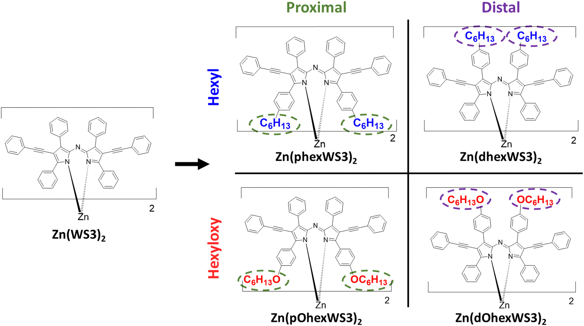 | ||
| Fig. 1 Chemical structures of the molecules investigated. | ||
Non-planar π-conjugated molecules have several advantages over planar molecules, including better solution processability, the ability to transport charges in several directions and the potential for unique photophysical and electronic properties that result from their twisted or curved shape.2,7 In OPVs, non-planar molecules also promote favourable phase separation with a π-conjugated polymer. One of the most common non-planar molecules in OPVs is [6,6]phenyl-C61-butyric acid methyl ester (PCBM).8–10 PCBM is a fullerene-derivative electron acceptor with good electron transport, 3 × 10⁻³ cm2 V−1 s−1.11 Its spherical shape facilitates phase separation with π-conjugated polymer donors and enables electron transport in all directions (isotropic), thus facilitating charge extraction in blend films.12 However, PCBM has several limitations that prompted the search for alternatives, the so called non-fullerene acceptors (NFAs). As a result, many non-planar electron acceptors (or n-type, electron transport materials) have been investigated, including dimers, trimers, and tetramers of planar π-conjugated molecules such as perylene diimide.13–15 The overall molecular shapes depend on the linker, which is typically organic/molecular. One example is PPDI shown in Fig. 2, which has a μe of ∼10−4 cm2 V−1 s−1.16
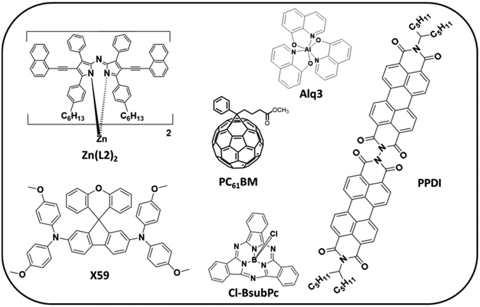 | ||
| Fig. 2 Examples of non-planar organic semiconductors mentioned in the text. | ||
Alternatively, one could use coordination with transition metals to access different molecular shapes. This approach is underexplored in the field or organic electronics, with only a few examples in the literature. This includes pyramidal subphthalocyanines such as Cl-BsubPc, used in vacuum deposited OPVs with an electron mobility (μe) of ∼10−5 cm2 V−1 s−1,17 octahedral Alq3 used as an electron transport layer material for OLEDs with a low μe of ∼10−5 cm2 V−1 s−1,18 and the distorted tetrahedral homoleptic metal(II) complexes of azadipyrromethenes (ADP), which we have used as electron acceptors in OPVs.6 Interestingly, our zinc(II) complexes of ADP can have a relatively high μe of ∼10−4 to 10−3 cm2 V−1 s−1,19,20 perhaps because these non-planar molecules are fully conjugated thanks to four intramolecular π–π stacking interactions between the two ligands.5
In terms of non-planar hole transport materials, there are fewer examples in the literature. One recent example is X59, a spiro[fluorene-9,9′-xanthene] based hole transport layer that gave a high efficiency perovskite photovoltaic with little hysteresis. This molecule has a low hole mobility (μh) of 5.5 × 10⁻⁵ cm2 V−1 s−1. Interestingly, our zinc(II) complexes of ADPs are also promising hole-transport materials. They exhibit two reversible oxidation events and the molecule Zn(L2)2, where naphthylethynyl groups were added to the ADP pyrrolic position, resulted in an ambipolar molecule with a μh of 1.0 × 10⁻⁴ cm2 V−1 s−1.21
Non-planar molecules tend to have lower charge carrier mobility because their non-planar nature may discourage order and long-range π–π stacking interactions in films. Inspired by work done with planar π-conjugated systems, we hypothesized that long-range order could be encouraged via strategic substitutions. For example, fluorination is known to increase π–π stacking and improve electronic properties in planar systems.22–26 We showed that fluorination can also be beneficial for non-planar systems: fluorination of the naphthylethynyl groups of Zn(L2)2 promotes co-facial interactions between the naphthylethynl groups of two adjacent molecules, leading to greater order and increase of both electron and hole mobility by an order of magnitude to 1 × 10⁻⁴ cm2 V−1 s−1 and 2 × 10⁻³ cm2 V−1 s−1, respectively.20
Another common method to guide film self-assembly and optimize charge transport of solution-processable π-conjugated materials is by optimizing the solubilizing groups nature, length, branching, and placement on the conjugated moiety, also known as side chain engineering.27–29 Side-chain engineering can be used to control steric hindrance, which affects solubility, conformation and molecular packing in films.30–33 The use of alkyl versus alkoxy groups has also been studied to optimize properties.34–37 The small substitution of methyl with oxygen in alkoxy groups can result in large differences in molecular packing, because oxygen is smaller than the methyl group and thus reduces steric hindrance.31 In addition, the alkoxy group shows the electron-donating conjugation effect, and can also introduce a dipole moment that may further guide molecular packing.35 While side chain engineering has been extensively used to optimize properties of planar π-conjugated molecules and polymers, its use in optimizing properties of non-planar molecules remains an understudied area.
Recently, we found that placing hexyl or hexyloxy solubilizing groups on the distal or proximal phenyls of Zn(WS3)2 (see chemical structures in Fig. 1) greatly affected their structural, electrochemical, thermal, and optical properties.38 Proximal phenyl substitutions lower oxidation potentials and red-shifted the absorption spectra compared to distal substitution, and the change was larger with the more electron donating hexyloxy groups. While Zn(WS3)2 is amorphous and does not form crystals, we were able to get crystal structures of all the substituted molecules. The crystal structures confirmed the typical distorted tetrahedral geometry of these types of complexes and show that the solubilizing groups on the distal phenyls extend away from the conjugated core whereas groups on the proximal phenyls are close to the other ligand's core. This placement affects the thermal properties: Differential scanning calorimetry shows that the distal substituted molecules have two endothermic peaks ascribed to melting of the side chain and main molecule, whereas the proximal substituted molecules have one crystallization peak and only one melting peak. In particular, the hexyloxy groups were found to drive self-assembly and crystallization much better than the hexyl groups. Polarized light microscopy showed long-range, feather-like crystals for Zn(dOhexWS3)2 and short-range, needle-like crystals for Zn(pOhexWS3)2 which we hypothesize should influence their charge transport properties compared to the hexyl substituted molecules which showed no observable features. In this work, we aim to understand how hexyl and hexyloxy solubilizing groups placed on the distal and proximal phenyls of Zn(WS3)2 affect film morphological and electrical properties.
Experimental
Materials
All chemicals were purchased from Sigma Aldrich or Fisher Scientific and used as received. The Zn(II) complexes were synthesized according to the literature procedures.38 The identity and purity of the compounds were confirmed via1H NMR and elemental analysis.Overlap integral calculations
To estimate the overlap integrals of our complexes, we performed single point energy calculations of the molecular pairs. The pairs were obtained from the crystal structure using Mercury 3.10.2. The charge transfer integral V was calculated using DFT in the Amsterdam density functional (ADF) code. To simplify the calculations, the hexyl side chains were manually replaced with methyl groups and the hexyloxy sidechains were replaced with methoxy groups in the ADF software. We followed the instructions for the tutorial from the SCM website (https://www.scm.com/applications/organic-electronics/electron-and-hole-mobilities-in-organic-electronics/). Each complex was manually defined as one fragment, for a total of two fragments. Single point calculations were performed using the GGA:PW91 functional, TZP basis set and no frozen core to guarantee an all-electron basis set. We also selected charge transfer integral properties, no symmetry and multilevel used fragments and checked charge and spin.Grazing-incident wide-angle X-ray diffraction (GIWAXD)
GIWAXD measurements were performed using the 11-BM complex materials scattering (CMS) beamline at the National Synchrotron Light Source II (NSLS-II), Brookhaven National Laboratory. The wavelength of the monochromatic X-ray beam was λ = 0.0918 nm (E = 13.5 keV). An area detector in-vacuum (Pilatus 800k) was used to collect GIWAXD patterns. Solutions of zinc materials (10 mg mL−1 in CHCl3 dissolved at 50 °C overnight) were filtered using a 0.20 μm PTFE filter onto cleaned silicon wafers (detergent, DI H2O, acetone, and 2-propanol (IPA) for 15 min each in the sonicator), spin coated using a Laurell Spin Coater WS-650 at 2000 rpm for 30 s and annealed for 125 °C for 15 min. Films were illuminated by the collimated X-ray beam at an incidence angle of 0.05–0.15°. The distance between sample and the detector was 261 mm, which was calibrated using silver behenate with the first-order reflection at a scattering vector of q = 1.076 nm−1. The data acquisition time for each GIWAXD sample was 20 s. xPolar (Stony Brook Technology and Applied Research, Inc., Stony Brook, NY) software was used for data processing and analysis.The morphology of as-cast and annealed films was studied by using GIWAXD. Diffraction patterns were treated using xPolar software and plotted as a function of the q-vector. Crystallite sizes were determined using the Scherrer equation:
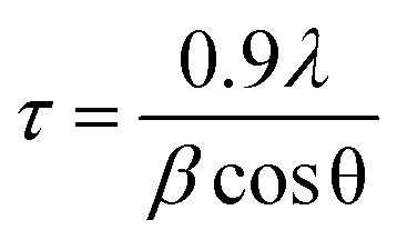 | (1) |
Diode mobility
The space-charge limited current (SCLC) method was used to measure the charge-carrier mobility of the Zn(II) complexes in neat films. Mobility was calculated under the SCLC trap-free conditions using the Mott–Gurney law: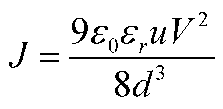 | (2) |
 | (3) |
For electron mobility device fabrication, ITO-coated glass slides were cleaned using detergent water, DI water, acetone, and IPA under sonication for 15 min, respectively. Slides were then dried with a nitrogen gun and cleaned under UV ozone treatment (PSDP-UV8T) at 85 °C for 15 min. Devices had the structure glass/ITO/ZnO/active material/Ca/Al. The glass slides were purchased pre-coated with ITO. A zinc acetate solution was made by combining 0.46 g zinc acetate, 5.0 mL 2-methoxyethanol, and 0.15 mL ethanolamine into a 20 mL vial on a hot plate stirring at 45 °C overnight. An additional 5.0 mL 2-methoxyethanol were added and stirred at 45 °C for 10 min. The ZnO was prepared by spin coating the zinc acetate solution at 4000 rpm for 1 min and annealed in air at 150 °C for 10 min. After deposition, the slides were cleaned using DI water, acetone, and IPA then dried with nitrogen. Each Zn complex was dissolved at 20 mg mL−1 in CHCl3 inside the nitrogen glove box (Pure LabHE) at 55 °C for 1 h. Each solution was filtered through a 0.45 μm PTFE filter prior to spin-coating at 800 rpm for 40 s then 2000 rpm for 2 s inside the glovebox. The devices were then annealed at 100 °C for 10 min. Finally, 30 nm calcium and 100 nm aluminum were deposited under vacuum using an Angstrom Engineering Evovac Deposition System. Hole mobility measurements were completed using the device structure glass/ITO/CuI/active material/MoO3/Ag. The copper iodide (CuI) layer was prepared using a 10 mg mL−1 solution of CuI in acetonitrile, spin coated at 4000 rpm for 30 s, and annealed at 100 °C for 10 min inside the glove box. The active material was prepared in the same way as the electron mobility devices. In the Angstrom system, 10 nm of MoO3 and 80 nm of Ag were thermally deposited. Finally, dark current measurements were completed inside the glovebox using a Keithley 2400 source meter. All devices had a total effective area of 0.2 cm2.
Organic thin-film transistor mobility
First, the gold source and drain pairs were patterned on a heavily n-doped SiO2/Si wafer with 300 nm thickness of SiO2 by conventional photolithography and thermal deposition. Then, the small square wafers that contained a set of transistors were cut from the large wafer and were placed into an aluminum dish (or a glass Petri dish, in either case) with acetone and sonicated in an ultra-sonic bath for 20 min at room temperature. Subsequently, acetone was removed, and IPA was added followed by ultrasonication for an additional 20 min. After sonication, the wafers were dried by using nitrogen gas and treated with oxygen plasma for 2 min with low air flow. Wafers were immersed into pure ethanol, chloroform, 20 mL of a 10 mM solution of octadecanethiol in ethanol for 1 hour and pure ethanol in a covered Petri dish successively. After that, wafers were immersed in 100 mL DI water in covered Petri dish, and four drops of 1![[thin space (1/6-em)]](https://www.rsc.org/images/entities/char_2009.gif) :10:10 (HNO3:HCl:H2O) were added. The wafers were kept for 1 min. Wafers were removed and rinsed with DI water. Wafers were dried with nitrogen gas and subsequently on a hot plate at 120 °C for 10 min. In the next step, wafers were put in a solution of 3% dodecyl trichlorosilane (DDTS) in toluene at room temperature for 20 min. The substrates were then rinsed with toluene to remove multilayers of DDTS and dried under a nitrogen flow. Then the solutions in chloroform (20 mg ml−1) were spin-coated onto the substrate at 2000 rpm for 60 s to obtain the films, which were further subjected to thermal annealing at different temperatures for 20 min in an argon filled glove box. All the OTFT devices have a channel length (L) of 30 μm and a channel width (W) of 1000 μm and were characterized in the same glove box using an Agilent B2912A Semiconductor Analyzer. The hole and electron mobilities are calculated in the saturation regime according to the following equation:
:10:10 (HNO3:HCl:H2O) were added. The wafers were kept for 1 min. Wafers were removed and rinsed with DI water. Wafers were dried with nitrogen gas and subsequently on a hot plate at 120 °C for 10 min. In the next step, wafers were put in a solution of 3% dodecyl trichlorosilane (DDTS) in toluene at room temperature for 20 min. The substrates were then rinsed with toluene to remove multilayers of DDTS and dried under a nitrogen flow. Then the solutions in chloroform (20 mg ml−1) were spin-coated onto the substrate at 2000 rpm for 60 s to obtain the films, which were further subjected to thermal annealing at different temperatures for 20 min in an argon filled glove box. All the OTFT devices have a channel length (L) of 30 μm and a channel width (W) of 1000 μm and were characterized in the same glove box using an Agilent B2912A Semiconductor Analyzer. The hole and electron mobilities are calculated in the saturation regime according to the following equation: | (4) |
Results and discussion
Crystal structure
The single crystal structures for the four complexes with solubilizing groups have been previously reported.38 All showed distorted tetrahedral geometry with the solubilizing groups either overlapping with the distal phenyls of the other ligand when placed on the proximal phenyls or extending away from the conjugated core when placed on the distal phenyls. Here, we further analyse the crystal packing of these molecules, with the goal of gaining insights into charge-transport properties.20,39 Tables S1–S4 (ESI†) shows calculated hole and electron overlap integrals (Vh+ and Ve−, absolute values) for all distinguishable pairs with |overlap integral| > 0.1, and Fig. 3 shows the adjacent pairs that have the largest calculated overlap integrals. According to the Marcus theory, charge transfer from one molecule depends on the electronic coupling (or overlap integral, V) and the reorganization energy.40 Since reorganization energy for these types of complexes are very small,41 charge transport in these molecules is expected to be limited by the overlap integrals. For the hexyl substituted molecules, Zn(phexWS3)2 had five distinct pairs, where several had significant overlap integrals, suggesting isotropic charge transport. The largest one has |Vh+| of 6.4 meV and |Ve−| of 1.6 meV. These overlap integrals are of similar magnitude to other Zn complexes we have published, and smaller compared to crystalline PCBM (up to 49 meV).42 For the distal substituted molecule, Zn(dhexWS3)2, we identified four distinct pairs with significant overlap integrals, covering all directions for charge transport. Close interactions between neighbouring molecules appear to be mostly “T-shaped”, which is expected for unsubstituted aryl groups. The pair illustrated in Fig. 3b has a |Vh+| of 3.9 meV and |Ve−| of 3.2 meV, with charge transport mostly in the X direction. Switching to the hexyloxy substituted molecules, Zn(pOhexWS3)2 has five distinct pairs with evidence for charge transport in several directions, like Zn(phexWS3)2. The dominant pair has |Vh+| of 3.8 meV and |Ve−| of 7.7 meV. The distal substituted molecule, Zn(dOhexWS3)2, has a very different crystal packing. While we identified four distinct pairs that cover all directions, one pair in the X, Y direction significantly dominates over the others, with |Vh+| of 17.9 meV and |Ve−| of 8.0 meV. The overlap integrals for the other three pairs are all less than 1.0 meV. This suggests a dominant linear path for charge transfer, where the phenylethynyl pyrrolic groups of adjacent molecules overlap somewhat cofacially and the hexyloxy are all aligned on each side, see Fig. 3d. Overall, these calculations suggest relatively small isotropic charge carrier mobilities, except for Zn(dOhexWS3)2, which may have higher charge carrier mobility in one dimension.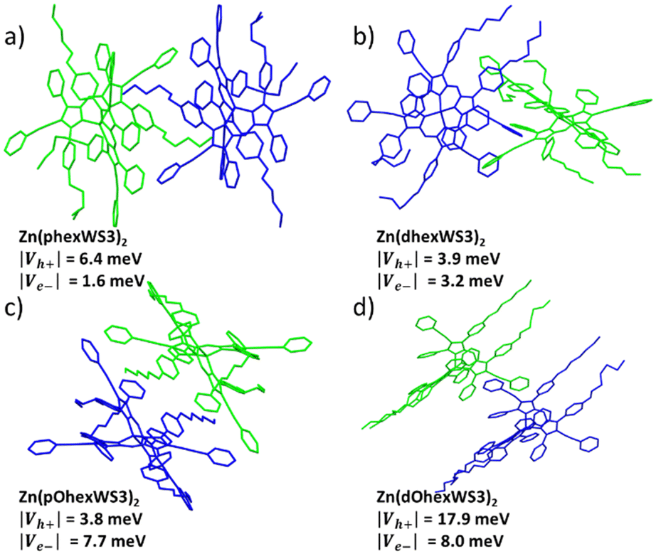 | ||
| Fig. 3 Adjacent pairs in a crystal packing lattice with largest calculated overlap integrals of (a) Zn(phexWS3)2, (b) Zn(dhexWS3)2, (c) Zn(pOhexWS3)2, and (d) Zn(dOhexWS3)2. | ||
GIWAXD study
Neat film morphology was examined by Grazing Incidence Wide Angle X-ray diffraction (GIWAXD). Fig. 4 shows the 2D GIWAXD patterns of the as-cast and annealed neat films and the intensities along the in-plane and out-of-plane directions versus the scattering vector, q. 2D GIWAXD patterns for Zn(phexWS3)2 (or Zn(L1)2) are provided in the ESI† of our previous study.21 The powder X-ray diffraction profiles calculated from the single crystallography data are shown in Fig. 4 (and also Fig. S1 in the ESI†) for comparison purposes. It appears that the GIWAXD reflections from the as-cast and annealed films do not match well with the powder profiles from the single crystal data, indicating that the crystal structures in films are somewhat different from those in single crystals.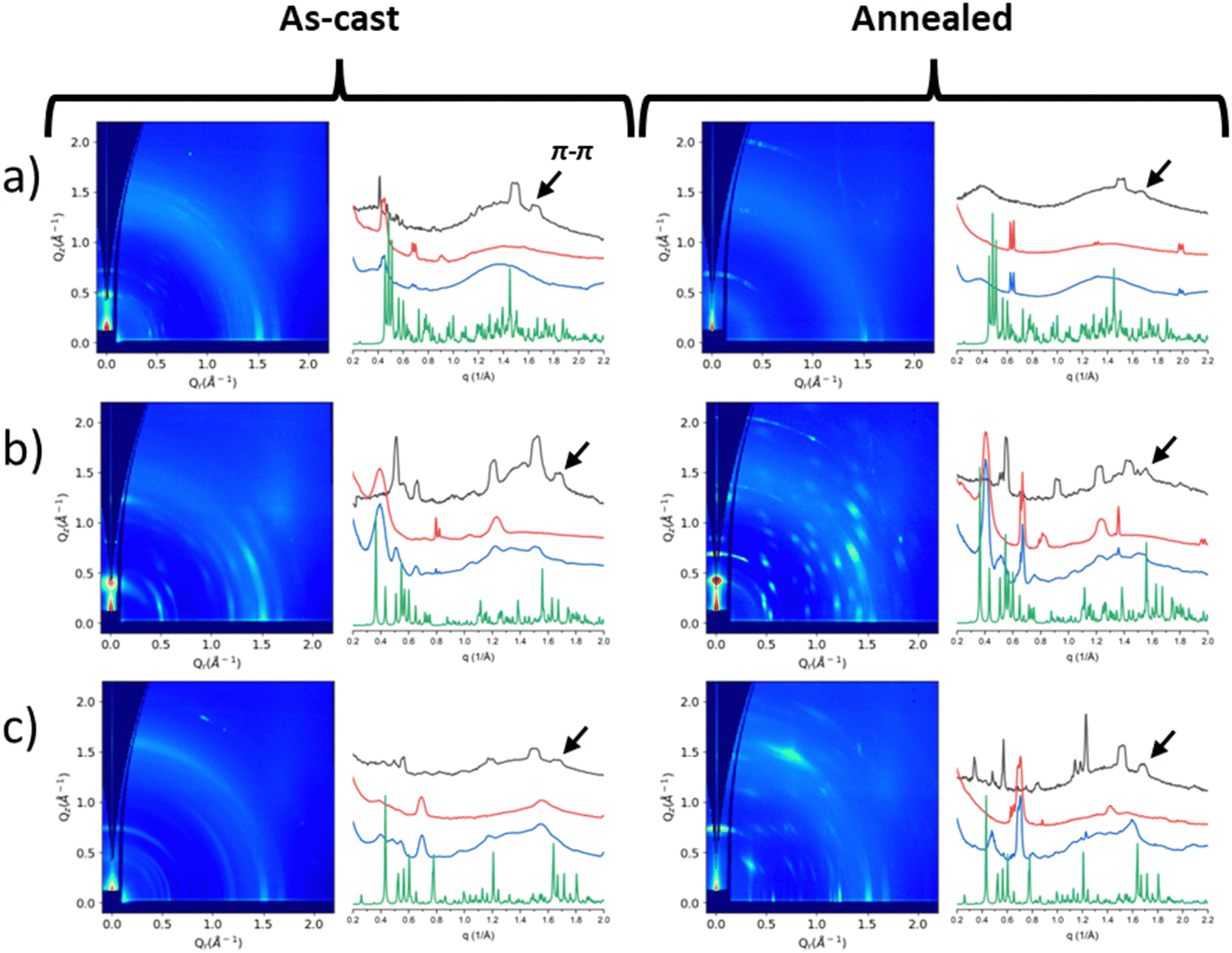 | ||
| Fig. 4 GIWAXD patterns and intensity vs. q plots of as-cast (left) and annealed (right) neat films of (a) Zn(dhexWS3)2, (b) Zn(pOhexWS3)2, and (c) Zn(dOhexWS3)2 with in-plane (black), out-of-plane (red), r (blue), and the powder diffraction (green). Arrows are used to indicate π–π stacking peaks. All y-axes are plotted logarithmically, except the powder diffraction which is plotted linearly. | ||
In the past, we studied similar systems where the π–π stacking distances were found to range between 3.6 and 3.9 Å.20 In this study, we selected reflections within this range to estimate the π–π stacking distances, as shown in Table 1. For the hexyl substituted molecule, Zn(phexWS3)2, the π–π stacking distance is constant for the as-cast and annealed films at ∼4.1 Å. For Zn(dhexWS3)2, the π–π stacking distance for the as-cast and annealed films is also constant and smaller, ∼3.8 Å. For the hexyloxy films, the π–π stacking distances change upon annealing. For Zn(pOhexWS3)2, the as-cast π–π stacking distance is 3.7 Å, which increases to 4.0 Å when annealed. Conversely, Zn(dOhexWS3)2, the as-cast π–π stacking distance is 3.8 Å, which slightly decreases to 3.7 Å when annealed.
| Compound | π–π Stacking (Å) | Crystallite size (nm) | ||
|---|---|---|---|---|
| As-cast | Annealed | In-plane | Out-of-plane | |
| Zn(phexWS3)2* | 4.1 | 4.1 | 13.9 | 13.9 |
| Zn(dhexWS3)2 | 3.8 | 3.8 | 7.4 | — |
| Zn(pOhexWS3)2 | 3.7 | 4.0 | 25.1 | 18.5 |
| Zn(dOhexWS3)2 | 3.8 | 3.7 | 41.9 | 16.7 |
The crystallite sizes in annealed films were estimated using the Scherrer equation from the strongest peak and reported in Table 1. Zn(phexWS3)2 has an estimated crystallite size in both in-plane and out-of-plane directions of ∼13.9 nm.21Zn(dhexWS3)2 has an estimated crystallite size of ∼7.4 nm in the in-plane direction, but was mostly amorphous in the out-of-plane direction. The proximal substituted molecule, Zn(pOhexWS3)2, has crystallite sizes in the in-plane and out-of-plane directions of ∼25.1 nm and ∼18.5 nm, respectively. The distal substituted molecule, Zn(dOhexWS3)2, has a crystallite size in the out-of-plane direction of ∼16.7 nm and much larger in-plane crystallite size than the proximal substituted molecule of ∼41.9 nm. Hexyloxy substitution on the distal phenyls thus results in larger crystallite sizes in the horizontal direction, consistent with the longer-range features previously observed by polarized light microscopy.38 To summarize this part, complexes with hexyl substitution have smaller crystallite sizes and poor crystal orientation even upon annealing whereas complexes with hexyloxy substitution show larger crystallite sizes with better order, and that order increases with annealing which could be beneficial for charge transport properties.
Diode mobility
The charge transport properties of the zinc complexes were estimated using the SCLC method. The μe was evaluated using the ITO/ZnO/complex/Ca/Al device configuration. For μh, we initially used the standard ITO/PEDOT:PSS/complex/MoO3/Ag device configuration but obtained poor results due to poor film formation. We then tried several alternative hole transport layers and found that CuI gave the best results.43 We therefore used the ITO/CuI/complex/MoO3/Ag device configuration for hole mobility measurements. The annealing conditions were optimized at a temperature of 100 °C for 10 min. Higher temperatures and/or longer annealing times resulted in aggregation and non-uniform films. The μe and μh were extracted from the SCLC region, and the average of at least 4 devices are given in Table 2 and illustrated in Fig. 5.| Complex | μ e (cm2 V−1 s−1) | μ h (cm2 V−1 s−1) |
|---|---|---|
| Zn(phexWS3)2 | (9 ± 4) × 10−4 | (1 ± 0.9) × 10−5 |
| Zn(dhexWS3)2 | (1 ± 1) × 10−4 | (2 ± 0.9) × 10−5 |
| Zn(pOhexWS3)2 | (6 ± 0.7) × 10−6 | (3 ± 2) × 10−3 |
| Zn(dOhexWS3)2 | (3 ± 2) × 10−4 | (4 ± 3) × 10−3 |
| Zn(WS3)2 | (1 ± 0.1) × 10−4 | (8 ± 4) × 10−6 |
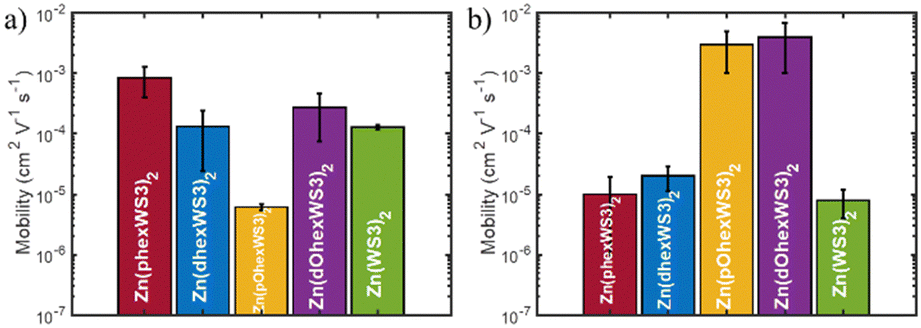 | ||
| Fig. 5 (a) Electron and (b) hole mobilities in diodes using the SCLC method. | ||
The average μe for Zn(WS3)2 was 1 × 10⁻⁴ cm2 V−1 s−1. Adding hexyl groups on the proximal phenyls significantly increased μe to 9 × 10⁻⁴ cm2 V−1 s−1, whereas adding hexyl groups on the distal phenyls did not change the μe value. On the other hand, hexyloxy substitutions significantly decreased the μe to 6 × 10⁻⁶ cm2 V−1 s−1 when placed on the proximal phenyls but increased μe slightly to 3 × 10⁻⁴ cm2 V−1 s−1 when placed on the distal phenyls. The nature of the solubilizing groups therefore has a strong influence on μe when placed on the proximal phenyls, where the solubilizing groups of one ligand are relatively close to the azadipyrromethene core of the other ligand. Here, the hexyloxy groups are detrimental to μe whereas the hexyl groups greatly enhanced μe. The μe for Zn(phexWS3)2 is thus very high and is comparable to that of PCBM.
The μh for the unsubstituted Zn(WS3)2 is low at 8 × 10⁻⁶ cm2 V−1 s−1. Adding hexyl groups either on the proximal or the distal phenyls slightly increases μh to 1 × 10⁻⁵ and 2 × 10⁻⁵ cm2 V−1 s−1 for Zn(phexWS3)2 and Zn(dhexWS3)2, respectively. These low values suggest that the unsubstituted and hexyl substituted molecules are poor hole conductors. In contrast, the μh for the hexyloxy substituted molecules are similar and significantly higher than the hexyl substituted molecules with a μh of 3 × 10⁻³ and 4 × 10⁻³ cm2 V−1 s−1 for Zn(pOhexWS3)2 and Zn(dOhexWS3)2, respectively. These are remarkably high μh values for non-planar molecules. Zn(pOhexWS3)2 is the best if only hole transport is desired, such as for hole transport layers. On the other hand, Zn(dOhexWS3)2 shows the best ambipolar performance with a μe and μh of 3 × 10⁻⁴ cm2 V−1 s−1 and 4 × 10⁻³, respectively.
Organic thin-film transistor mobility
The electronic properties of the complexes were also investigated in organic thin-film transistors (OTFTs). The power transfer and output graphs are shown in the ESI,† and the μe and μh results for as-cast spin-coated films are summarized in Table 3 and Tables S6 and S7 (ESI†). We have no data for Zn(WS3)2 because of poor film formation. Annealing devices at 50 °C or 100 °C worsened the film quality due to self-aggregation. As a result, annealing decreased the mobility in all cases except for the μe of Zn(dOhexWS3)2 when annealed at 50 °C for 20 min under argon (value added to Table 3). Generally, these complexes do not show high charge carrier mobilities in OTFTs, suggesting that they do not self-assemble favorably on the dodecyl trichlorosilane treated SiO2 dielectric interface. The power output curves show that the materials have many traps, which is consistent with film defects. Nevertheless, data show that the μe is strongly influenced by the identity of the solubilizing group at the proximal position, as seen in diodes: Zn(phexWS3)2 has the highest μe of 2 × 10⁻⁴ cm2 V−1 s−1 whereas Zn(pOhexWS3)2 has the lowest μe of 3 × 10⁻⁶ cm2 V−1 s−1. While these values are slightly lower than in diodes, they are of the same order of magnitude, consistent with isotropic charge transport. The μe for Zn(dhexWS3)2 and the best mobility for Zn(dOhexWS3)2 are 7 × 10⁻⁵ and 2 × 10⁻⁴ cm2 V−1 s−1, respectively, which are similar to the diode values, also consistent with isotropic charge transport.Unlike what was observed in diodes, all molecules exhibited similar μh, with a value of ∼10−5 cm2 V−1 s−1. The μh values of the hexyl substituted molecules are similar in both transistors and diodes, consistent with isotropic charge transport and confirm that hexyl groups are unfavorable for hole transport. However, the μh values of the hexyloxy substituted molecules are two orders of magnitude lower than in diodes. This suggests that hexyloxy groups favor charge transport in the z direction.
Conclusions
Analysis of the crystal packing suggests that all complexes should have isotropic charge transport except for the molecule with hexyloxy groups on the distal phenyls, Zn(dOhexWS3)2, which may have higher charge transport in one dimension. GIWAXD shows hexyl substitution tends to produce smaller crystallites with poor crystal orientation, while hexyloxy substitution leads to more crystalline and ordered films, with increased order upon annealing. However, the microstructure of thin films differs from that of single crystals, limiting our ability to explain charge transport using the crystal packing analysis. The nature and placement of the solubilizing groups have a notable impact on charge carrier mobility. In diodes, hexyl substitutions, especially on the proximal phenyls, promote electron transport whereas hexyloxy substitutions at either position promote hole transport. Interestingly, the nature of the solubilizing group on the proximal phenyls strongly influenced the μe of these complexes, with a very high μe of 9 × 10⁻⁴ cm2 V−1 s−1 for Zn(phexWS3)2 compared to a very low μe of for Zn(pOhexWS3)2. This may be because the substitutions on the proximal phenyls are close to the core of the other ligand in the complex. We did not observe any dramatic changes in μe when the substitutions were on the distal phenyls. Hexyl substituted molecules had low μh whereas hexyloxy substituted molecules had very high μh, amongst the highest μh estimated by SCLC method to our knowledge. Zn(pOhexWS3)2 only transports holes well whereas Zn(dOhexWS3)2 is ambipolar, with both high electron and hole mobilities. In field-effect transistors, extracted charge carrier mobilities were generally lower than in diodes, perhaps due to less favorable self-assembly and film-formation of these complexes on the dodecyl trichlorosilane treated SiO2 dielectric surface. Nevertheless, results suggest that hexyl substitution promote isotropic charge transport whereas hexyloxy substitution may favor charge transport across the film. This study highlights the importance of the nature and placement of solubilizing groups in optimizing the charge transport properties of these non-planar molecules for different applications.Author contributions
Lexi Knight: performed characterization of complexes in diodes, GIWAXD processing, formal analysis, and manuscript writing. Jayvic C. Jimenez: responsible for the GIWAXD measurements, contributed to crystal structures, synthesis of all complexes, conception and formal analysis. Quynh Tran: performed synthesis of all complexes. Muyuan Zhao: performed initial characterization of complexes in diodes. Madison H. Pugh: contributed to synthesis of complexes. Christina D. Brancel: contributed to crystal structures. Honghu Zhang: responsible for GIWAXD measurements. Ruipeng Li: responsible for GIWAXD measurements. Yi Yuan: performed characterization of complexes in transistors. Yuning Li: formal analysis. Lei Zhu: formal analysis. Geneviève Sauvé: responsible for conception, project management, formal analysis and manuscript writing.Data availability
The data supporting this article have been included as part of the ESI.†Conflicts of interest
There are no conflicts to declare.Acknowledgements
We are grateful to the National Science Foundation (CHEM 19048678 and 2203595) for funding this project. This work was performed in part under the auspices of the U.S. Department of Energy by Lawrence Livermore National Laboratory under Contract DE-AC52-07NA27344, LLNL-JRNL-856960. This research used the 11-BM CMS beamline of the National Synchrotron Light Source-II (NSLS-II), Brookhaven National Laboratory (BNL), a U.S. Department of Energy User Facility operated for the Office of Science by BNL under Contract DE-SC0012704.References
- Y. Ge and D. F. O'Shea, Chem. Soc. Rev., 2016, 45, 3846–3864 RSC
.
- R. Kumar, H. Aggarwal and A. Srivastava, Chem. – Eur. J., 2020, 26, 10653–10675 CrossRef CAS PubMed
- M. Lorenz-Rothe, K. S. Schellhammer, T. Jägeler-Hoheisel, R. Meerheim, S. Kraner, M. P. Hein, C. Schünemann, M. L. Tietze, M. Hummert and F. Ortman, Adv. Electron. Mater., 2016, 2, 1600152 CrossRef
- W. Senevirathna and G. Sauvé, J. Mat. Chem. C, 2013, 1, 6684–6694 RSC
- T. S. Teets, D. V. Partyka, J. B. Updegraff Iii and T. G. Gray, Inorg. Chem., 2008, 47, 2338–2346 CrossRef CAS PubMed
- Z. Mao, W. Senevirathna, J. Y. Liao, J. Gu, S. V. Kesava, C. Guo, E. D. Gomez and G. Sauvé, J. Adv. Mater., 2014, 26, 6290–6294 CrossRef CAS PubMed
- D. Li, X. Zhang, D. Liu and T. Wang, J. Mater. Chem. A, 2020, 8, 15607–15619 RSC
- M. T. Dang, L. Hirsch and G. Wantz, J. Adv. Mat., 2011, 23, 3597–3602 CrossRef CAS PubMed
- C. J. Brabec, S. Gowrisanker, J. J. Halls, D. Laird, S. Jia and S. P. Williams, Adv. Electron. Mater., 2010, 22, 3839–3856 CAS
- L. Lu, T. Zheng, Q. Wu, A. M. Schneider, D. Zhao and L. Yu, Chem. Rev., 2015, 115, 12666–12731 CrossRef CAS PubMed
- M.-A. Muth, W. Mitchell, S. Tierney, T. A. Lada, X. Xue, H. Richter, M. Carrasco-Orozco and M. Thelakkat, Nat. Nanotechnol., 2013, 24, 484001 CrossRef PubMed
- A. M. Nardes, A. J. Ferguson, P. Wolfer, K. Gui, P. L. Burn, P. Meredith and N. Kopidakis, Chem. Phys. Chem., 2014, 15, 1539–1549 CrossRef CAS PubMed
- G. Zhang, J. Zhao, P. C. Chow, K. Jiang, J. Zhang, Z. Zhu, J. Zhang, F. Huang and H. Yan, Chem. Rev., 2018, 118, 3447–3507 CrossRef CAS PubMed
- S. Li, Z. Zhang, M. Shi, C.-Z. Li and H. Chen, Phys. Chem. Chem. Phys., 2017, 19, 3440–3458 RSC
- H. Sun, X. Song, J. Xie, P. Sun, P. Gu, C. Liu, F. Chen, Q. Zhang, Z.-K. Chen and W. Huang, ACS Appl. Mater. Interfaces, 2017, 9, 29924–29931 CrossRef CAS PubMed
- L. Ye, K. Sun, W. Jiang, S. Zhang, W. Zhao, H. Yao, Z. Wang and J. Hou, ACS Appl. Mater. Interfaces, 2015, 7, 9274–9280 CrossRef CAS PubMed
- G. E. Morse and T. P. Bender, ACS Appl. Mater. Interfaces, 2012, 4, 5055–5068 CrossRef CAS PubMed
- C. W. Tang and S. A. VanSlyke, Appl. Phys. Lett., 1987, 51, 913–915 CrossRef CAS
- S. Pejić, A. M. Thomsen, F. S. Etheridge, R. Fernando, C. Wang and G. Sauvé, J. Mater. Chem. C, 2018, 6, 3990–3998 RSC
- M. Zhao, J. C. Jimenez, C. Wang, G. Rui, T. Ma, C. Lu, A. L. Rheingold, R. Li, L. Zhu and G. Sauvé, J. Phys. Chem. C, 2022, 126, 6543–6555 CrossRef CAS
- C. Wang, P. Wei, J. H. Ngai, A. L. Rheingold, T. G. Gray, Y. Li, E. Pentzer, R. Li, L. Zhu and G. Sauvé, J. Mater. Chem. A, 2019, 7, 24614–24625 RSC
- K. Reichenbächer, H. I. Süss and J. Hulliger, Chem. Soc. Rev., 2005, 34, 22–30 RSC
- Q. Zhang, M. A. Kelly, N. Bauer and W. You, Acc. Chem. Res., 2017, 50, 2401–2409 CrossRef CAS PubMed
- J.-H. Dou, Y.-Q. Zheng, Z.-F. Yao, Z.-A. Yu, T. Lei, X. Shen, X.-Y. Luo, J. Sun, S.-D. Zhang and Y.-F. Ding, J. Mater. Chem. A, 2015, 137, 15947–15956 CAS
- B. Maiti, A. Schubert, S. Sarkar, S. Bhandari, K. Wang, Z. Li, E. Geva, R. J. Twieg and B. D. Dunietz, Chem. Sci., 2017, 8, 6947–6953 RSC
- Q. He, M. Shahid, X. Jiao, E. Gann, F. D. Eisner, T. Wu, Z. Fei, T. D. Anthopoulos, C. R. McNeill and M. Heeney, ACS Appl. Mater. Interfaces, 2020, 12, 9555–9562 CrossRef CAS PubMed
- J. Mei and Z. Bao, Chem. Mater., 2014, 26, 604–615 CrossRef CAS
- Y. Yang, Z. Liu, G. Zhang, X. Zhang and D. Zhang, J. Adv. Mater., 2019, 31, 1903104 CrossRef CAS PubMed
- S. Kraner, J. Widmer, J. Benduhn, E. Hieckmann, T. Jägeler-Hoheisel, S. Ullbrich, D. Schütze, K. Sebastian Radke, G. Cuniberti and F. Ortmann, Phys. Status Solidi, 2015, 212, 2747–2753 CrossRef CAS
- R. D. McCullough and R. D. Lowe, J. Chem. Soc., Chem. Commun., 1992, 70–72 RSC
- H. Zhou, L. Yang, S. Xiao, S. Liu and W. You, Macromolecules, 2010, 43, 811–820 CrossRef CAS
- K. R. Graham, C. Cabanetos, J. P. Jahnke, M. N. Idso, A. El Labban, G. O. Ngongang Ndjawa, T. Heumueller, K. Vandewal, A. Salleo and B. F. Chmelka, J. Am. Chem. Soc., 2014, 136, 9608–9618 CrossRef CAS PubMed
- H. Bronstein, D. S. Leem, R. Hamilton, P. Woebkenberg, S. King, W. Zhang, R. S. Ashraf, M. Heeney, T. D. Anthopoulos and J. d Mello, Macromolecules, 2011, 44, 6649–6652 CrossRef CAS
- C. Cui and W. Y. Wong, Macromol. Rapid Commun., 2016, 37, 287–302 CrossRef CAS PubMed
- D. Zhu, Q. Zhu, C. Gu, D. Ouyang, M. Qiu, X. Bao and R. Yang, Macromolecules, 2016, 49, 5788–5795 CrossRef CAS
- H.-H. Chang, C.-E. Tsai, Y.-Y. Lai, W.-W. Liang, S.-L. Hsu, C.-S. Hsu and Y.-J. Cheng, Macromolecules, 2013, 46, 7715–7726 CrossRef CAS
- J. Zhu, Y. Xiao, J. Wang, K. Liu, H. Jiang, Y. Lin, X. Lu and X. Zhan, Chem. Mater., 2018, 30, 4150–4156 CrossRef CAS
- J. C. Jimenez, Q. Tran, M. H. Pugh, C. D. Brancel, A. L. Rheingold and G. Sauvé, Dyes Pigm., 2022, 208, 110858 CrossRef CAS
- W. Zhu, A. P. Spencer, S. Mukherjee, J. M. Alzola, V. K. Sangwan, S. H. Amsterdam, S. M. Swick, L. O. Jones, M. C. Heiber and A. A. Herzing, J. Am. Chem. Soc., 2020, 142, 14532–14547 CrossRef CAS PubMed
- W.-Q. Deng, L. Sun, J.-D. Huang, S. Chai, S.-H. Wen and K.-L. Han, Nat. Protoc., 2015, 10, 632–642 CrossRef CAS PubMed
- W. Senevirathna, C. M. Daddario and G. Sauvé, J. Phys. Chem. Lett., 2014, 5, 935–941 CrossRef CAS PubMed
- F. Gajdos, H. Oberhofer, M. Dupuis and J. Blumberger, J. Phys. Chem. Lett., 2013, 4, 1012–1017 CrossRef CAS PubMed
- W. Sun, S. Ye, H. Rao, Y. Li, Z. Liu, L. Xiao, Z. Chen, Z. Bian and C. Huang, Nanoscale, 2016, 8, 15954–15960 RSC
Footnote |
| † Electronic supplementary information (ESI) available. See DOI: https://doi.org/10.1039/d4ma00313f |
| This journal is © The Royal Society of Chemistry 2024 |