DOI:
10.1039/D4MA00780H
(Paper)
Mater. Adv., 2024,
5, 9488-9499
A high-performance broadband organic flexible photodetector from a narrow-bandgap thiazolo[5,4-d]thiazole containing conjugated polymer
Received
2nd August 2024
, Accepted 30th October 2024
First published on 31st October 2024
Abstract
Our present study developed high-performance organic photodetectors (OPDs) with broad-spectrum capabilities utilizing a thiazolo[5,4-d]thiazole containing a high-mobility conjugated polymer P-TZTZ. The low bandgap polymer with 2D nanosheet morphology is synthesized by an easy condensation reaction between dithiooxamide and terephthalaldehyde. Based on the used substrate (Si-wafer and PET substrate), two variants of the proposed photodetectors were fabricated. Both variants of the fabricated photodetectors (PDs) demonstrated comparable photodetection capabilities in a broad region from 400 to 1000 nm. Under the presence of a broadband white light source, the peak photo-to-dark current ratio (PDCR) values for the PD fabricated on Si-substrate (PD1) are calculated to be 42.58 and 5.68 at the bias voltage (VB) of −0.1 and +1.0 V, respectively. Similarly, the PD fabricated on ITO-coated PET substrate (PD2) under the influence of a broadband white light source offered PDCR values of 8.65 and 7.25 at a VB of −4 V and +4 V, respectively. Experimental findings indicate that the fabricated PD1 achieves a peak responsivity of 2.12 A W−1 at 410 nm with peak external quantum efficiency (EQE) values of 6.41% and 4.32% at 410 and 530 nm, respectively. The specific detectivity (D) values are estimated to be 4.42 × 10¹³ Jones at 410 nm and 3.71 × 10¹³ Jones at 530 nm. Similarly, the fabricated PD2 achieves the peak responsivity, external quantum efficiency, and specific detectivity values of 1.98 A W−1, 5.9% and 1.71 × 10¹³ Jones at 410 nm, respectively. Transient performance analysis revealed that the P-TZTZ-based flexible PD exhibited rise and fall times of 180 ms and 100 ms, respectively. The high responsivity, detectivity, and millisecond-order switching time in rigid and flexible P-TZTZ-based PDs demonstrate the versatility and potential for diverse applications covering from rigid to flexible electronics.
1. Introduction
Conventional panchromatic photodetectors (PDs) exceed in measuring light intensity and providing spectral information about objects. However, for a deeper understanding of surface features like shading, roughness, and material properties, detecting light's polarization state or phase offers invaluable insights.1 Polarization-resolved PDs, capable of simultaneously capturing intensity and phase information, reveal various applications ranging from polarization division multiplexing communication to remote sensing, quantum optics, and medical diagnosis.2–4 Traditionally, achieving polarization detection involves adding optical polarization components to conventional PDs or employing arrays of detectors. However, this approach significantly increases system complexity, size, and cost while compromising sensitivity and responsiveness.5 An alternative approach takes advantage of semiconductor materials' intrinsic anisotropic optoelectronic properties, eliminating the need for external optics. Certain low-dimensional semiconductors, such as one-dimensional nanowires (e.g., InP) and two-dimensional materials (e.g., MoS2, SbS2, GeSe2, etc.), exhibit inherent anisotropic light absorption and polarized photo-response, showcasing the promising potential for polarization-resolved PDs.6–8 Nonetheless, challenges persist, including the complex growth of oriented nanowires and the production of bulk 2D materials.9 Moreover, PDs based on low-dimensional semiconductors sometimes suffer from high dark current, low detectivity, and sluggish detection speed, often requiring operation under a reverse bias voltage.
Organic semiconductors have emerged as compelling candidates for photodetection applications due to their adjustable detection wavelength and sensitivity to weak light, enabling diverse applications such as lightwave communications, night vision, environmental monitoring, bio-sensing, etc.10–13 The spectral response of these materials can be finely tuned by modifying the chemical structure of the active layer. While many polymeric materials offer tunable bandgaps (Eg) and photoelectric properties by altering the topology and periodicity of the precursor, those constructed from relatively small aromatic subunits, such as conjugated polymers and covalent organic frameworks, often exhibit wider bandgaps, favouring absorption of the high-energy portion of visible light.14–16 However, polymers with narrower bandgaps, high carrier mobility, and enhanced electrical conductivity are fascinating for optoelectronic devices and broadband PDs. Polymeric materials can be engineered to address these requirements by stacking or arranging donor–acceptor organic subunits within the framework building blocks.17 Conjugated polymers, in particular, offer versatility and mechanical flexibility, making them ideal for the cost-effective, solution-based fabrication of thin, flexible, and large-surface-area organic photodetectors (OPDs) capable of multicolour detection.18,19 Despite the challenges associated with the low solubility of high-molecular-weight copolymers, their extended conjugation length facilitates enhanced π–π stacking within a bi-continuous network, thereby improving hole mobility.5 Conjugated polymers employing electron-rich (donor) and electron-deficient (acceptor) building blocks exhibit robust light absorption, high charge motilities, and exceptional power conversion efficiencies in applications such as organic photovoltaics (OPVs) and organic field-effect transistors (OFETs).20–22 Their rigid, planar backbone promotes strong intermolecular interactions in the solid state, facilitating high charge mobilities and making them promising candidates for OPDs with rapid photoresponse.21,22
Integrating the versatility of heterocyclic units into organic conjugated polymers holds significant promise for advancing the performance of organic photodetectors.23–32 Organic semiconducting polymers are ideal for photodetectors due to their tunable bandgaps, enabling broad spectral absorption from visible to NIR regions and enhancing multi-wavelength detection. Their flexibility and mechanical durability support integration with bendable substrates. These polymers are solution-processable, allowing cost-effective, large-scale production techniques like inkjet printing. The π-conjugated structures improve charge mobility and responsivity, boosting sensitivity and the response time. Heterocyclic cores (e.g., thiophene) and heteroatoms (e.g., nitrogen, sulfur) further optimize charge transport, bandgap tuning, and material stability, making them highly suited for high-performance flexible photodetectors. This innovative strategy influences the distinctive electronic and optical properties inherent to heterocycles, affording unprecedented control over device functionality and efficiency. In this context, a series of organic conjugated polymers including polyaniline (PANI), poly(3-hexylthiophene) (P3HT), polypyrrole (Ppy), polyvinylcarbazole (PVK), and poly(3,4-ethylenedioxythiophene) are investigated for their potential in photodetection applications.23–28,33–35 However, there is always the scope to introduce innovative conjugated heterocycle-containing polymers into the arena of photodetection for further development. Additionally, the development of flexible organic polymer-based photodetectors offers several advantages and challenges. Flexibility allows these devices to be integrated into unconventional applications, such as wearable electronics, foldable displays, and curved surfaces, due to their mechanical adaptability. Additionally, their lightweight nature and compatibility with low-cost, large-area fabrication methods, such as roll-to-roll printing, make them attractive for scalable production. However, flexibility can introduce disadvantages, including reduced charge mobility, lower responsivity, and decreased device efficiency, as mechanical strain may impact the polymer's electronic properties. Furthermore, repeated bending can lead to mechanical fatigue, reducing device longevity, while the polymers’ inherent sensitivity to moisture, oxygen, and UV light necessitates robust encapsulation, which adds complexity to the design. Balancing these factors is crucial for optimizing the performance and durability of flexible photodetectors.
The fused aromatic bicyclic thiazolo[5,4-d]thiazole (TZTZ), synthesized via a simple condensation reaction between dithiooxamide and aldehyde, emerges as a versatile class of heterocyclic compounds with multifunctional attributes across various domains such as chemosensors, biosensors, field-effect transistors, light-harvesting dyes, and photovoltaics.29–32 The extended conjugation facilitated by the rigid TZTZ moiety enhances electronic communication, resulting in a remarkably high charge carrier mobility (∼3 cm2 V−1) when combined with different conjugated derivatives in copolymers.36,37 This exceptional charge carrier mobility, coupled with the semiconducting nature of TZTZ moieties, underscores the suitability of TZTZ-based conjugated polymers for a diverse array of electronic applications.38,39 In this study, we have developed a TZTZ-containing polymer, P-TZTZ, which acts as an active layer to fabricate a thin film broadband PD. This organic polymer was synthesized using the simple condensation reaction to provide the P-TZTZ as a near-infrared absorbing low optical bandgap polymer. Exploiting the inherent semiconducting nature with the high charge carrier mobility of TZTZ and taking advantage of the self-assembly of TZTZ moieties in the polymer to provide flexible 2D nanosheets, two PDs were fabricated by P-TZTZ in two different substrates. The first PD1 was fabricated on a rigid Al-coated p-type Si substrate, whereas the second PD2 was fabricated on a flexible ITO-coated PET substrate. In both cases, the basic structure of the fabricated PD is a metal–semiconductor–metal (MSM) junction, which efficiently collects the photogenerated electron–hole pairs (EHPs). The fabricated OPDs exhibited a decreased dark current and enhanced external quantum efficiency (EQE). The combination of these merits leads to a remarkable detectivity of 4.42 × 10¹³ Jones and a responsivity of 2.12 A W−1 at a wavelength of 410 nm for PD1 and those for PD2 are 1.71 × 10¹³ Jones at 410 nm and 1.98 A W−1 at 410 nm, demonstrating one of the best results reported so far in OPDs. Detailed material characterization and electrical and photodetection study coupled with a plausible explanation of the operational principles of the proposed PDs with the help of a suitable energy band diagram can provide a comprehensive understanding of the rationale for designing and potential of TZTZ-containing polymer-based broadband OPDs.
2. Experimental section
2.1 Materials
1,4-Benzenedicarboxaldehyde (terephthalaldehyde), dithiooxamide, tetrabutylammonium perchlorate (TBAP), acetonitrile (ACN), methanol (MeOH), ethanol (EtOH) and dimethyl formamide (DMF) were obtained from Sigma Aldrich Co. Ltd. The indium tin oxide (ITO)-coated PET substrates (with a resistance of 20 Ω) and p-type silicon wafer used in our study were provided by Shilpa Enterprises.
2.2 Instrumentation
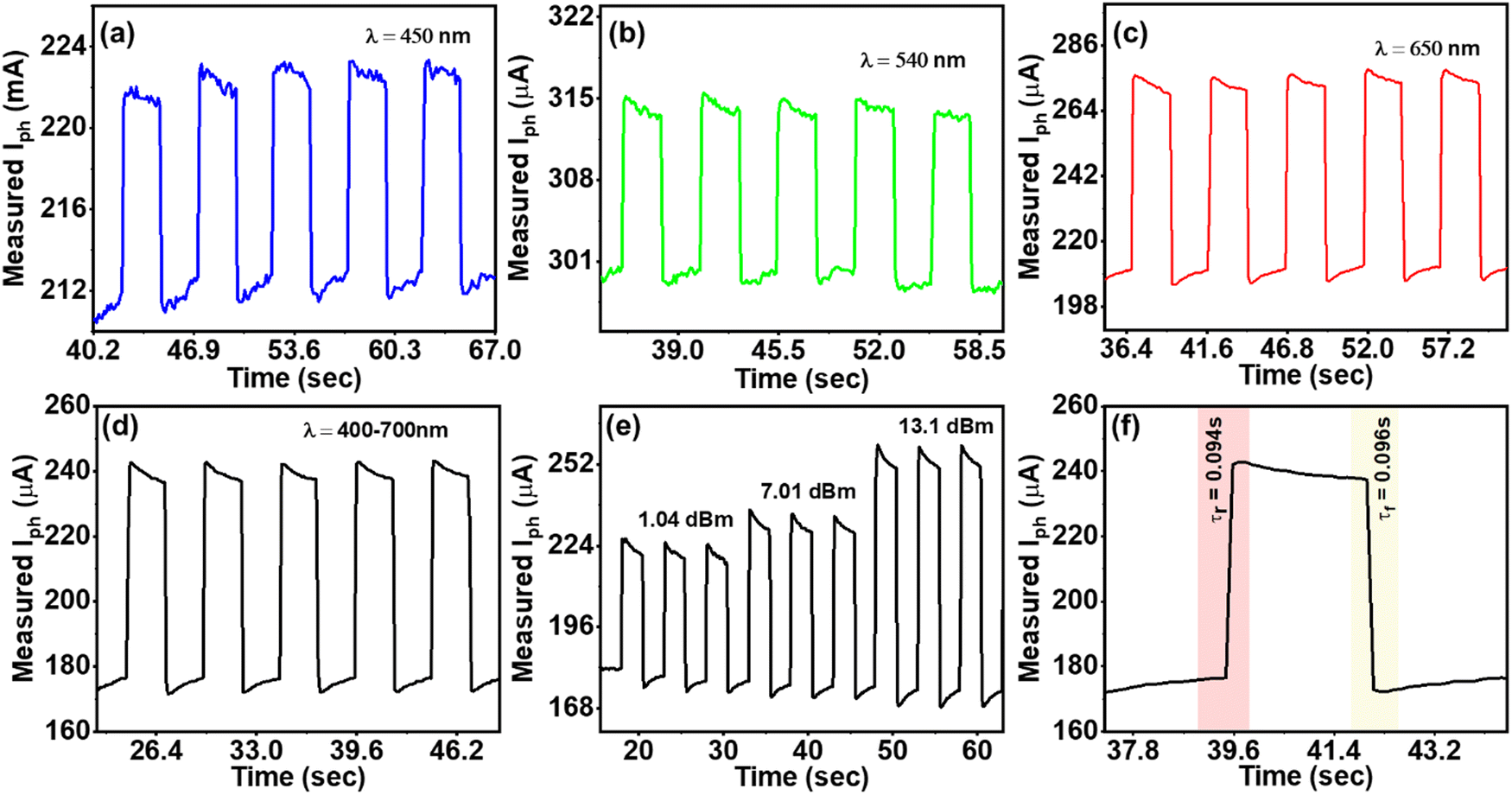
The solid-state UV-vis absorption and emission spectra of P-TZTZ were obtained using a JASCO/V-650 (190–900 nm) UV-vis spectrophotometer and a JASCO/FP-6300 (190–900 nm) spectrofluorometer. A JASCO/FTIR-4200 spectrometer was used to collect the FTIR spectra of P-TZTZ, using KBr pellets of P-TZTZ. The morphological analysis of P-TZTZ powder and the cross-sectional thickness measurement of P-TZTZ films in PDs were carried out via field emission scanning electron microscopy (FESEM) using an FEI Apreo SEM instrument operating at 30 kV. The X-ray photoelectron spectra (XPS) were recorded using a Thermo Scientific Multilab 2000 with Al Kα radiation (1486.6 eV) at 15 kV and 10 mA (150 W), referencing all binding energies to C 1s at 284.85 eV. Background correction was performed using Avantage software (Avantage 5.9931) with smart background correction. The electrochemical characterization of P-TZTZ was done using an Autolab PGSTST128N potentiostat utilizing a three-electrode cell where P-TZTZ coated GCE, Ag/AgCl in saturated KCl, Pt wire, and 0.1 M TBAP/ACN were used as the working electrode, reference electrode, counter electrode, and electrolyte, respectively. Additionally, the DC electrical characterization of the fabricated devices was conducted using a Keithley 2450 source meter through a DC probe station. The various photodetection performance metrics were estimated using an automated PD characterization setup (Holmarc PDC 5000S) with a 50 W tungsten halogen lamp as a broadband light source, directed through a Czerny–Turner monochromator and second-order filters to achieve a wavelength tuning range from 350 nm to 1600 nm. The photodetection was performed by preparing a device of ∼4 mm2. For the study of the time-dependent photoresponse of fabricated prototypes, four light sources of wavelengths λ = 450 nm with an input power of Pin = 3.01 dBm, λ = 540 nm with an input power of Pin = 3.89 dBm, λ = 650 nm with an input power of Pin = 5.11 dBm and broadband white light source with an input power of Pin = 17.01 dBm were used.
2.3 Synthesis of P-TZTZ
P-TZTZ was prepared according to our previous report.40 In a typical poly-condensation reaction, as shown in Fig. 1a, terephthalaldehyde (600 mg, 4.47 mmol) and dithiooxamide (538 mg, 4.47 mmol) were dissolved in 20 mL of dry DMF, and the reaction mixture was refluxed for 12 hours under an inert atmosphere. Subsequently, the reaction mixture was cooled to room temperature, and excess MeOH was added to obtain a precipitate. The precipitate was filtered and washed with different solvents like water, methanol, and diethyl ether. Finally, the product was dried in a vacuum at 70 °C to obtain 770 mg (80% yield) of the polymer. GPC study: Mw 10 kDa and PDI = 1.7. FT-IR: 1653 cm−1 (C![[double bond, length as m-dash]](https://www.rsc.org/images/entities/char_e001.gif) N stretching), 1505 cm−1, 1558 cm−1, 1601 cm−1 (CC vibration of the aromatic ring), and 1007 cm−1 (C–S stretching of the TZTZ ring).
N stretching), 1505 cm−1, 1558 cm−1, 1601 cm−1 (CC vibration of the aromatic ring), and 1007 cm−1 (C–S stretching of the TZTZ ring).
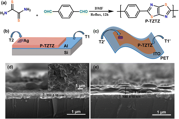 |
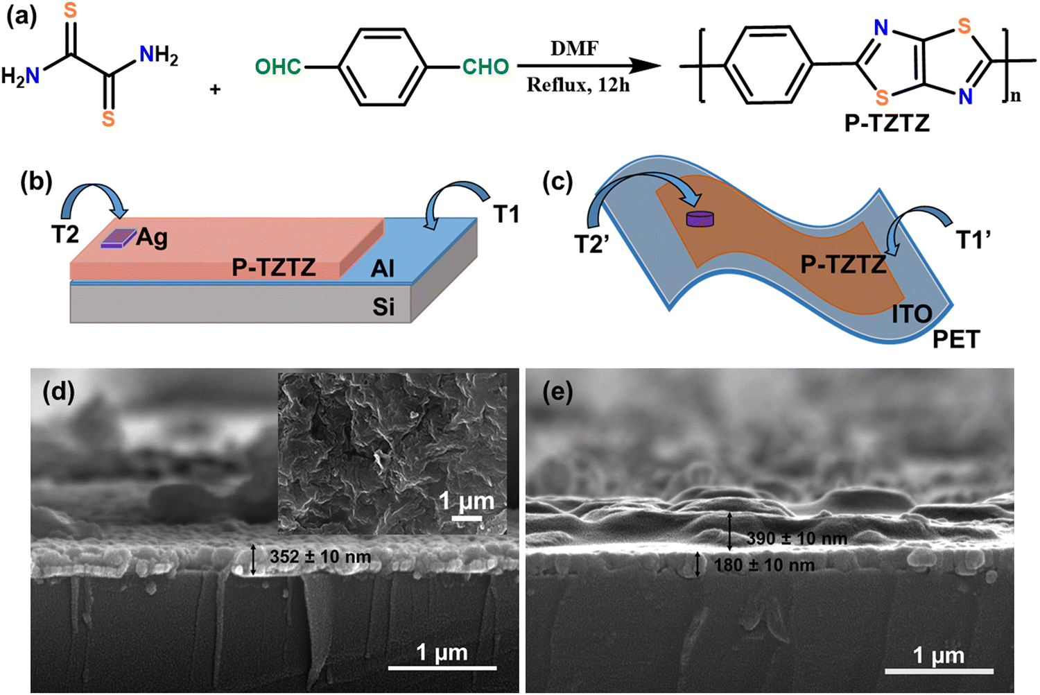
| | Fig. 1 (a) Synthesis and chemical structure of P-TZTZ. Schematic of the fabricated P-TZTZ-based photodetectors on (b) a rigid Si substrate (PD1) and (c) on a flexible ITO-coated PET substrate (PD2). Cross-sectional HR-SEM images of (d) PD1 and (e) PD2. The inset of (d) shows uniform deposition of the synthesized polymer. | |
2.4 Device fabrication for photodetector application
Initially, a p-type silicon wafer underwent cleaning through the RCA-1 method, followed by the deposition of a 100 nm thick aluminium (Al) layer using the electron-beam evaporation technique. This Al layer served as one of the electrodes (T1 electrode, as shown in Fig. 1b) for the fabricated PD1. Subsequently, a portion of the Al layer was encapsulated and a thin layer of synthesized P-TZTZ was coated via the spin-coating technique (4 mg mL−1 in methanol, 500 rpm for 60 s), resulting in a P-TZTZ-based thin film with a film thickness of 352 ± 10 nm, as shown in Fig. 1d. Furthermore, the device was subjected to a temperature of 60 °C in a hot air oven for 15 minutes to dry the active layer properly. The Ag-based top electrode was then deposited using shadow masking and thermal evaporation (with an electrode thickness of 100 ± 10 nm), thereby establishing an MSM structure for the fabricated PD1. ITO-coated PET was selected as the substrate for the flexible version of the proposed PD2. The ITO layer on this substrate functioned as one of the electrodes (T1′ electrode as shown in Fig. 1c). A section of the substrate was encapsulated, and P-TZTZ solution (4 mg mL−1 in methanol) was spin-coated at 500 rpm for 60 seconds on a 1 cm × 1 cm ITO-coated PET substrate to provide a P-TZTZ film of 390 ± 10 nm (Fig. 1e). Subsequently, the device was kept overnight at 60 °C in a hot air oven. The second electrode (T2′) was formed using Ag-paste to complete the PD2. Given the fabrication of two PDs, the one on the Si-substrate (rigid PD-1) and the ITO-coated PET substrate (flexible PD-2) will be denoted as PD1 and PD2 throughout the article.
3. Results and discussion
3.1 Synthesis and characterization of P-TZTZ
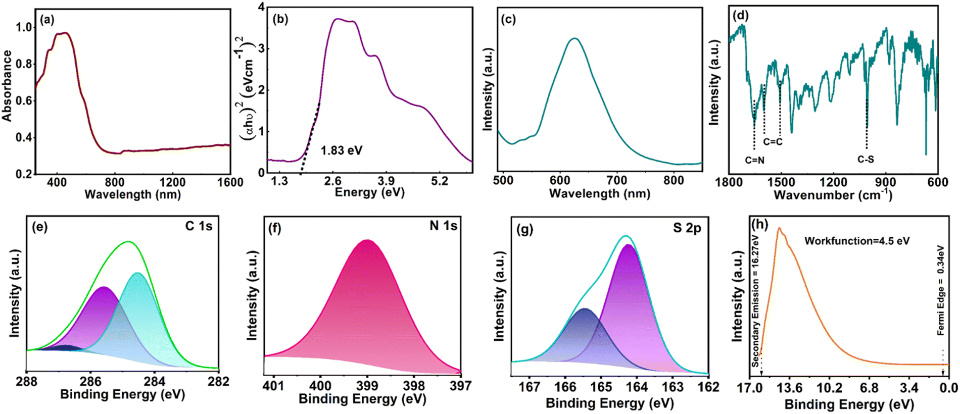
The TZTZ containing conjugated copolymer P-TZTZ was synthesized by the condensation reaction between the dithiooxamide and terephthalaldehyde, taking a 1![[thin space (1/6-em)]](https://www.rsc.org/images/entities/char_2009.gif) :1 molar ratio under refluxing conditions using anhydrous DMF as the solvent according to the scheme shown in Fig. 1a. The molecular weight determination using the GPC study revealed the Mw of P-TZTZ to be 10 kDa and the synthesized copolymer was thoroughly characterized by different spectroscopic techniques, bonding environment analyses and morphological studies. The solid-state UV-vis spectra of P-TZTZ in Fig. 2a reveal a broad absorption in the range of approximately 300–700 nm, with a peak maximum at 460 nm, associated with the π–π* transition within the conjugated polymer structure and the wide absorption band around 300–700 nm is attributed to the extensive π-electron conjugation in the conjugated polymers. The bandgap of the P-TZTZ polymer was evaluated by the Tauc plot employing the Kubelka–Munk function and extrapolation of the tangent to the energy axis as given in Fig. 2b. The bandgap (Eg) value of P-TZTZ was determined to be 1.83 eV from the Tauc plot. The broad absorption spectra and low bandgap of P-TZTZ advocated its application towards wide-band photodetector and optoelectronic applications. The P-TZTZ powder displayed emission peaks at ∼630 nm (Fig. 2c) due to the S1–S0 transition in the conjugated polymer system. The FTIR spectrum (given in Fig. 2d) showcased distinctive peaks at 1653 and 1007 cm−1 corresponding to the CN and C–S stretching frequency within the P-TZTZ. The peaks at 1505, 1558, and 1601 cm−1 were also attributed to the CC vibration present in the aromatic benzene unit. The strong peak at 1005 cm−1 indicated a stretching frequency of the C–S bonds in the TzTz units of the polymer.
:1 molar ratio under refluxing conditions using anhydrous DMF as the solvent according to the scheme shown in Fig. 1a. The molecular weight determination using the GPC study revealed the Mw of P-TZTZ to be 10 kDa and the synthesized copolymer was thoroughly characterized by different spectroscopic techniques, bonding environment analyses and morphological studies. The solid-state UV-vis spectra of P-TZTZ in Fig. 2a reveal a broad absorption in the range of approximately 300–700 nm, with a peak maximum at 460 nm, associated with the π–π* transition within the conjugated polymer structure and the wide absorption band around 300–700 nm is attributed to the extensive π-electron conjugation in the conjugated polymers. The bandgap of the P-TZTZ polymer was evaluated by the Tauc plot employing the Kubelka–Munk function and extrapolation of the tangent to the energy axis as given in Fig. 2b. The bandgap (Eg) value of P-TZTZ was determined to be 1.83 eV from the Tauc plot. The broad absorption spectra and low bandgap of P-TZTZ advocated its application towards wide-band photodetector and optoelectronic applications. The P-TZTZ powder displayed emission peaks at ∼630 nm (Fig. 2c) due to the S1–S0 transition in the conjugated polymer system. The FTIR spectrum (given in Fig. 2d) showcased distinctive peaks at 1653 and 1007 cm−1 corresponding to the CN and C–S stretching frequency within the P-TZTZ. The peaks at 1505, 1558, and 1601 cm−1 were also attributed to the CC vibration present in the aromatic benzene unit. The strong peak at 1005 cm−1 indicated a stretching frequency of the C–S bonds in the TzTz units of the polymer.
 |
| | Fig. 2 Material characterization of the synthesized P-TZTZ: (a) the solid-state UV-vis and (b) emission spectra of the P-TZTZ polymer, (c) Tauc plot indicating Eg, (d) FTIR spectra, (e) XPS core level scan of the C 1s, (f) N 1s and (g) S 2p, and (h) UPS spectra showing the work function of the synthesized P-TZTZ. | |
The bonding connectivity at the surface of P-TZTZ was further evaluated by XPS studies. The C 1s core level spectrum in Fig. 2e exhibits three distinct peaks at 284.5, 285.5, and 286.7 eV, likely attributed to the presence of aromatic sp2 C, C atom within the thiazole linkage, and S-bonded C centers in P-TZTZ moieties, respectively. The N 1s spectrum in Fig. 2f reveals a single dominant peak at 398.9 eV, attributed to the imine-N in TZTZ moieties. The core-level S 2p spectrum in Fig. 2g discloses the fitting into two distinct peaks: S 2p3/2 (164.2 eV) and S 2p1/2 (165.5 eV). The work function (φ) of the synthesized copolymer P-TZTZ was measured at 4.5 eV using ultraviolet photoelectron spectroscopy (UPS) and is shown in Fig. 2h. The morphology of P-TZTZ was studied by FESEM analysis, and the corresponding images are presented in Fig. 3a. The P-TZTZ powder exhibited a bulk 2D nanosheet structure with an average thickness of ∼25 nm for the nanosheet. This observation suggested the presence of extensive π–π stacking between the 1D nanorods of P-TZTZ, resulting in the formation of a 2D nanosheet within the solid polymer. Also, the elemental mapping, as shown in Fig. 3b, indicated an even distribution of all the elements (C, N, and S) across the entirety of the polymer surface. EDX analysis of the powder P-TZTZ polymer, including high-resolution mapping, also showed uniform distribution of N and S throughout the polymeric surface, and the homogenous carbon distribution was obtained due to the P-TZTZ carbon and background carbon tape. Moreover, the SEM images displayed a very smooth polymeric surface. We performed STM to thoroughly investigate the surface roughness and morphological features of the nanosheet. As illustrated in Fig. 3c, the analysis revealed an average roughness of approximately 14.4 nm across the nanosheet surface. This relatively low roughness value confirms a smooth and uniform morphology, which is crucial for applications where surface quality impacts the material's functional performance. In nanostructured materials, especially those used in catalysis, electronics, or energy storage devices, surface roughness can influence key parameters such as the charge carrier mobility, chemical reactivity, and catalytic activity. A smoother surface typically reduces scattering events, defects, and grain boundaries, all of which can degrade performance.
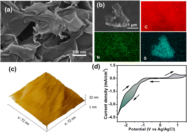 |
| | Fig. 3 (a) The FESEM image of the P-TZTZ polymer. (b) The EDX elemental mapping of the polymer. (c) STM image and (d) cyclic voltammogram of the P-TZTZ film on GCE. | |
The electrochemical characterization of the P-TZTZ film was conducted via cyclic voltammetry (CV), using P-TZTZ coated GCE as the working electrode and 0.1 M TBAP/ACN as the electrolyte. P-TZTZ displayed a quasi-reversible single electron reduction at an Ered of −1.64 V and the corresponding oxidation at an Eox of 0.8 V due to the radical anion formation of thiazole[5,4-d]thiazole units.40 Taking the reduction onset at 0.97 V and optical bandgap at 1.83 eV, we have derived the lowest unoccupied molecular orbital (LUMO) of the P-TZTZ as −3.34 eV and the highest occupied molecular orbital (HOMO) as −5.17 eV.41–43 These obtained HOMO and LUMO values are utilized in the band diagram to explain the photodetection mechanism later in this article.
3.2 Photodetector response
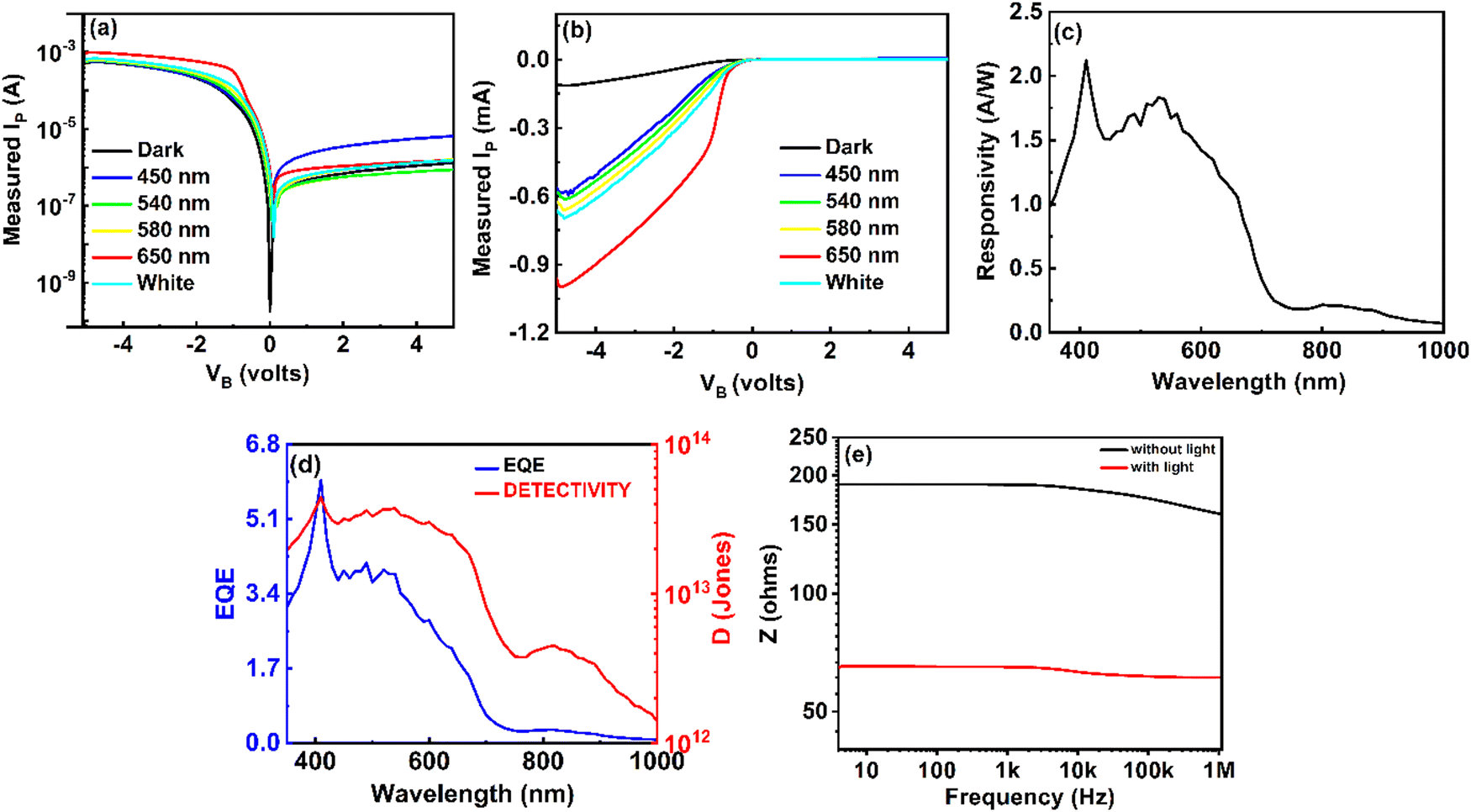
The I–V characteristics of both the PDs were determined by varying the applied bias voltage (VB) in the range of ±5 V. The I–V features of the fabricated device were assessed both in the absence and in the presence of a photoexcitation source. For this experiment, both PD1 and PD2 were connected to a source measuring unit (Keithley 2450) via a DC probe station. Additionally, this study utilized a broadband white light source and four different light sources at specific wavelengths in the visible band (λ = 450 nm, 540 nm, 580 nm, and 650 nm). In every instance of photoexcitation, the input optical power (Pin) was consistently set at 5 dBm and monitored using a standard optical power meter (Thorlabs PM400D). The combined I–V characteristics, both in linear and logarithmic scales, are depicted in Fig. 4a and b, respectively. The experimental results indicate that the nonlinearity observed in the I–V curve originated from the modulation of the Schottky barrier (SB) formed at the interfaces between the metal and the semiconductor. Without photoexcitation, the dark current (ID) of the PD1 device was measured as 52.5 nA and 93.2 nA at VB = −0.1 V and +1.0 V, respectively, demonstrating a negligible dark current. The lower dark current in the proposed PD can be attributed to the formed SBs near the electrodes. For the flexible device (PD2), the dark current was 2.2 μA and 22.14 μA at VB = −4 V and +4 V, respectively. Under white light photoexcitation, PD1 exhibited photocurrents (IP) of 2.29 μA and 0.63 μA with an external VB of −0.1 V and +1.0 V, respectively. Therefore, the photo-to-dark current ratios (PDCRs) were calculated from the following eqn (1):| |  | (1) |
where the ID and IP are the measured current through the PD in the absence and in the presence of external photoexcitation, respectively. Consequently, the calculated values of PDCR for PD1 under white light excitation are 42.58 and 5.68, at VB values of −0.1 and +1.0 V, respectively. Furthermore, the calculated PDCR values for PD1 at 650 nm photoexcitation were found to be 52.82 and 8.69 for VB = −0.1 V and +1.0 V, respectively. Additionally, the abovementioned analysis suggests that the PDCR for PD1 was better for VB < 0 V, indicating a favourable operating condition for PD1 under reverse-biased conditions.
 |
| | Fig. 4 Electrical characterization of fabricated PD: measured I–V characteristics of PD1 in (a) the logarithmic scale and (b) the linear scale. (c) Measured R in the 380 nm to 1000 nm range. (d) Measured EQE and calculated D values in the 380 nm to 1000 nm range. (e) Impedance analysis of PD1. | |
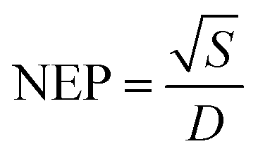
The experimental setup facilitated the measurement of several key parameters of the photodetector, including responsivity (R), external quantum efficiency (EQE), detectivity (D), and linearity of PDs. Throughout the metrics assessment, the feedback resistance of the trans-impedance amplifier (TIA) remained constant at 100 kΩ. The observed R values for PD1, spanning wavelengths from 350 nm to 1000 nm, are presented in Fig. 4c. At 410 nm, PD1 exhibited a peak R-value of 2.12 A W−1, with another corresponding peak at 530 nm, measuring 1.83 A W−1. Beyond 800 nm, the PD1 device displayed measured R values below 1 A W−1 (≈ 0.145 A W−1 at 900 nm). An intriguing observation was the non-zero R for λ > 677 nm, which found an explanation in the internal photoemission process.16 For wavelengths shorter than the bandgap energy (hν > Eg), incident radiation triggers electron–hole pair generation within the active layer, contributing significantly to the internal photoemission process. However, for longer wavelengths (where qφB < hν < Eg), some incident photons were absorbed within the metal electrodes, leading to the generation of ‘hot’ electrons. These electrons, possessing excess energy surpassing the barrier height, contributed actively to IP, explaining the non-zero R in the NIR region. Noise-equivalent power (NEP) is a critical parameter in assessing the performance of a PD. It represents the input power level that generates an output signal power equal to the inherent internal noise of the device. NEP quantifies the sensitivity of the photodetector by defining the threshold at which the desired signal becomes indistinguishable from the device's intrinsic noise. The NEP can be derived from the following eqn (2):
| |  | (2) |
For PD1, the estimated value of NEP is 2.86 × 10
−9 W Hz
−1/2. Clearly the result indicates that PD1 can swiftly detect and provide highly sensitive photoresponses even when exposed to signals of low-power intensity. Similarly, the device (as depicted in
Fig. 4d) achieved a peak EQE of 6.41% and 4.32% at 410 and 530 nm, respectively. Beyond 850 nm, the PD1 device exhibited a drop in EQE of 0.19% at 900 nm. Detectivity (
D), is an important fundamental metric, commonly used to measure the sensitivity of any PD. Generally, the detectivity can be calculated using the following
eqn (3):
| |  | (3) |
where
S represents the active area of the PD (∼3 mm
2), and
e signifies the electronic charge. The
D values for PD1 were estimated and are plotted in
Fig. 4d. The peak value of
D is 4.42 × 10
13 Jones at 410 nm and 3.71 × 10
13 Jones at 530 nm, respectively. Notably, the device exhibited significant detectivity at >800 nm (3.02 × 10
12 Jones at 900 nm). These results highlight the comparable performance of the proposed PD1 for detecting weak optical signals. Frequency-dependent impedance analysis of the proposed PD1 was also done using an impedance analyzer. The results, as shown in
Fig. 4e, illustrate a clear change in the device resistance under different photoexcitation conditions. The estimated resistance values of the PD1 in the absence and in the presence of photoexcitation are 180.1 Ω and 52.2 Ω, respectively. Since the change in device resistance under photoexcitation is approximately 3.45 times, it is expected that the proposed device will exhibit a high PDCR value. As the characteristic frequency of PD1 is well beyond 1 MHz, it can be inferred that the deposited thin film had very few defects.
44,45
The time-dependent photo-response characteristics of PD1 were systematically investigated in the subsequent phase of experimentation by recording their temporal behaviour. This study utilized an intensity-modulated light source across varying wavelengths to assess the transient behaviour of PD1. For achieving the modulation of the light source, the driver circuitry was provided with a square wave input with specific parameters including a peak-to-peak amplitude of −2 V, a time period of 0.5 s, and a duty cycle of 50%. Similar to the DC characterization, Pin was measured using a Thorlabs PM400D optical power meter. Fig. 5a–e depicts the temporal responses of PD1 at different operating wavelengths. As depicted in Fig. 5f, the measured 10%-to-90% rise time (τr) and 90%-to-10% fall time (τf) for the device were determined at 94 ms and 96 ms, respectively. The abovementioned observation signifies the exceptional stability of the proposed PD when subjected to different intensities of input photoexcitation. Notably, both τr and τf were recorded within the range of milliseconds. Thus, the demonstrated organic broadband photodetector showcases a remarkable achievement, exhibiting high responsivity and detectivity and a millisecond switching time, underscoring its potential for applications demanding swift and sensitive light detection in diverse fields of research and technology.
 |
| | Fig. 5 Temporal characteristics of the fabricated P-TZTZ-based rigid PD1: (a) at λ = 450 nm with Pin = 3.01 dBm, (b) at λ = 540 nm with Pin = 3.89 dBm, and (c) at λ = 650 nm with Pin = 5.11 dBm, (d) broadband white light source, (e) with varying Pin for broadband white light source and (f) transient performance. | |
In the pursuit of advancing photodetection technologies in wearable electronics, a PET substrate-based flexible photodetector using the same P-TZTZ was prepared and named PD2 (Fig. 6a). The previously achieved remarkable performance of PD1 on an Si-based rigid substrate encouraged us to move our focus to adapt similar capabilities to flexible OPD platforms, which promise increased adaptability and applicability in a variety of developing fields. The resulting combined I–V characteristics, displayed in Fig. 6b and c in both linear and logarithmic scales, revealed a similar and the measured dark current (ID) for PD2, demonstrating minimal dark current. At a bias voltage of −0.1 V without any light illumination, the current was only 2.2 μA and under λ = 650 nm light illumination, a current of 69.8 μA was observed for flat conditions. Under white light photoexcitation, the PDCR value of PD2 was calculated to be 8.65 and 7.25 at VB = −4 V and +4 V, respectively. Additionally, the PDCR ratio at 650 nm light was determined to be 16.52 and 12.97 at VB = −4 V and +4 V, respectively. Utilizing the same setup as discussed earlier, the R values of PD2 were observed to be 1.98 A W−1 at 410 nm, 1.68 A W−1 at 540 nm (in Fig. 6d) and a similar non-zero response beyond 800 nm (≈ 0.137 A W−1 900 nm). The NEP value of PD2 was estimated to be 2.33 × 10⁻⁸ W Hz−1/2. The highest EQE of PD2 was observed to be 5.9% at 410 nm, as shown in Fig. 6e. Utilizing the above eqn (3), the D values of PD2 were calculated to be 1.71 × 10¹³ Jones at 410 nm and 2.34 × 10⁸ Jones at 1000 nm. Interestingly, under bending conditions (bending angle 7°) there is a drastic decrement in the photocurrent to 1.57 μA. This decrement in the photocurrent may be due to a decrease in the active region attributed to bending conditions.46,47 On further bending the device (bending angle 26°), there is an increment in the photocurrent to 20.4 μA. When the device is subjected to further bending (bending angles 32° and 34°), there is a further increment in the photocurrent to 38.97 μA and then a slight decrement in the photocurrent to 27.67 μA. The increase in the photocurrent may be due to the bending strain, which seems to have a significant influence on the conductance of the device due to the tunable bandgap of the material.48–50 Similarly, through the time-dependent photoresponse characteristics, the measured values of τr and τf of PD2 were found to be 180 ms and 100 ms, respectively (refer to Fig. 6f). The change in average rise and fall time between PD1 and PD2 was observed, attributed to variations in the substrate and electrode configurations influencing the surface barrier height and electron–hole pair mobility within the PDs which is further explained in the next segment through a band diagram. PD2 was fabricated on a PET substrate and underwent rigorous optoelectronic testing under repeated bending under light conditions. Throughout the testing phase, PD2 devices were systematically bent up to a 65° angle, subject to 500 bending cycles, and the results obtained are represented in Fig. 6g and h. The measured I–V characteristics exhibited remarkable resilience; bending up to 65° did not significantly alter the measured photocurrent (Fig. 6g). Remarkably, the continuous bending up to 500 cycles at 65° also did not exhibit much change in photocurrent, as depicted in Fig. 6h. Additionally, we have compared the photodetector response of PD2 with some recently reported flexible devices in Table 1. This analysis validates the photodetector's suitability for application, showcasing its robustness and performance superiority, particularly in the face of mechanical strain induced by bending.
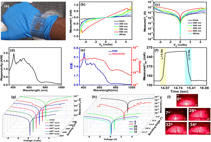 |
| | Fig. 6 (a) Digital image of the fabricated flexible and wearable PD2. Electrical characterization of fabricated PD2: measured I–V characteristics of PD2 in (b) the linear scale and (c) the logarithmic scale. Measured (d) R, (e) EQE and D in the 400 nm to 1000 nm wavelength range. (f) The transient performance of PD2. Electrical characterization of PD2 with respect to different (g) bending cycles and (h) bending angles and (i) the images of PD2 at different bending angles under a 650 nm light source. | |
Table 1 Comparison of photodetector performance of recently reported flexible devices
| Year |
Active material |
Synthesis procedure |
Substrate |
λ (nm) |
R (A W−1) |
D (Jones) |
τ
r (s) |
τ
f (s) |
Ref. |
| 2020 |
TAPP-TEPP-COF |
Solvothermal |
ITO |
>400 |
— |
— |
— |
— |
51
|
| 2020 |
P(PDI-BDT-O) |
|
SiO2/Si |
633 |
212 |
2 × 10¹² |
— |
— |
52
|
| 2021 |
AlaNDI-Ca MOF |
Solvothermal |
SiO2/Si |
365–808 |
0.65 |
— |
150 |
163 |
53
|
| 2021 |
P3HT:PC61BM |
RF magnetron sputtering sol–gel |
SiO2/Si |
365 |
0.58 |
3.67 × 10¹² |
— |
— |
54
|
| 2021 |
PCDTPTSe:PC71BM |
Solution process |
Glass |
660–1510 |
|
>1011 |
|
100 × 10−9 |
55
|
| 2022 |
SnO2/ZrBDC |
Solution process |
PET |
254 |
0.0017 |
7.85 × 10¹⁰ |
0.08 |
0.15 |
56
|
| 2023 |
ZnO/Ni-CAT COF |
Hydrothermal |
SiO2/Si |
450 |
0.132 × 10⁻³ |
— |
0.003 |
0.05 |
57
|
| 2023 |
TpDPP |
Solution process |
FTO |
380–700 |
0.4387 |
0.794 × 10¹⁰ |
— |
— |
58
|
| 2023 |
TPATZTPA |
Condensation reaction |
PET |
350–950 |
5.69 |
1.27 × 10¹¹ |
0.29 |
0.28 |
16
|
| 2024 |
P-TZTZ |
Condensation reaction |
Al, PET |
350–950 |
21.98 |
1.71 × 10¹³ |
0.18 |
0.10 |
Present work |
3.3 Principle of operation
This section explains the operational principles of PD1 and PD2 using energy band diagrams. To construct the energy band diagram, we first determined the HOMO and LUMO energy levels of the polymer through a CV study, found to be −5.17 eV and −3.34 eV, respectively, resulting in an energy band gap of 1.83 eV (as depicted in Fig. 2c). The polymer's work function, measured via ultraviolet photoelectron spectroscopy (UPS), was 4.5 eV. Additionally, UPS analysis of the aluminium (Al) bottom electrode and silver (Ag) top electrode provided work functions of 4.2 eV and 4.7 eV, respectively. Based on these values, the E–B diagram was constructed, assuming a vacuum level of 0 eV, with energy levels plotted below this as negative values. Fig. 7(a) shows the flat energy levels of the rigid photodetector (PD) before contact, where P-TZTZ has not interacted with the electrodes. In contrast, Fig. 7(c) illustrates the band-bending that occurs after contact at the junctions formed between Al and P-TZTZ (J1), and between P-TZTZ and Ag (J2). Upon contact, the Fermi levels unify, causing the other energy levels to shift accordingly. Charge carrier transport at the interface results in band-bending, while regions far from the junction remain flat. Fig. 7(b) and (d) depict similar diagrams for the flexible PD, using PET-ITO as the substrate with its standard work function of 4.8 eV. Notice that, a Schottky barrier forms near the Al–P-TZTZ interface, while an ohmic junction forms near the Ag–P-TZTZ interface. As a result, a built-in electric field is expected near the Al–P-TZTZ electrode. Upon photoexcitation, the active layer generates electron–hole pairs; while PD1 collects electrons at the T1 (Al) electrode and holes at the T2 (Ag) electrode, PD2 collects electrons at the T1′ (ITO) electrode and holes at the T2′ (Ag) electrode. The bias voltages adjust the depletion region width, thereby reinforcing the built-in electric field and facilitating the separation of photogenerated electron–hole pairs. This configuration amplifies the Iph, a phenomenon corroborated by the observed I–V characteristics of both PD1 and PD2.
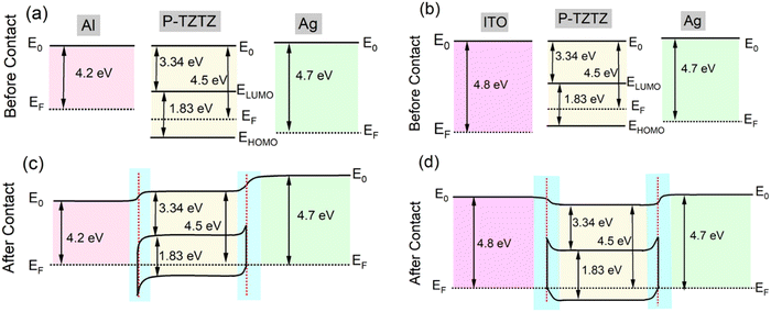 |
| | Fig. 7 Energy-band diagram of fabricated PDs under equilibrium conditions: (a) PD1 before contact, (b) PD2 before contact, (c) PD1 after contact, and (d) PD2 after contact. | |
3.4 Application in a visible lightwave communication system
To assess the efficacy of the proposed polymer-based PD herein for on chip applications, the fabricated PD1 underwent rigorous testing within a visible light communication (VLC) experimental framework. The setup employed a broadband light source positioned approximately 50 cm from PD1, modulated by a PN9 pseudo-random bit sequence (PRBS) with a peak-to-peak amplitude of 2 V and an 8.4 ns edge time. This modulated light passed through a collimator before being focused onto PD1. Connected to a Keithley 2450 source meter, PD1 recorded the detected signal. Fig. 8a illustrates the schematic of the VLC setup. The resulting photo-detected signal output, depicted in Fig. 8b, confirmed the PD1's ability to successfully detect the transmitted PRBS pattern. Moreover, as previously discussed, enhancements in VLC system data rates are achievable through integrating appropriate charge transport layers and meticulous optimization of the active layer thickness.
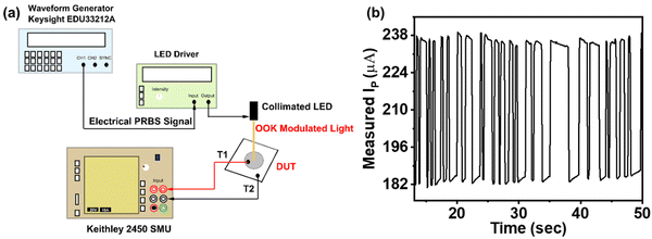 |
| | Fig. 8 Application of the fabricated PDs in visible lightwave communication: (a) experimental setup and (b) detected PRBS pattern measured using a Keithley 2450 SMU. | |
4. Conclusions
In summary, we have successfully synthesized a thiazole[5,4-d]thiazole-containing conjugated organic copolymer (P-TZTZ) by applying a simple polycondensation technique. The synthesized P-TZTZ was thoroughly characterized using optical spectroscopy, morphology analysis, and electrochemical studies. The low bandgap (1.83 eV), inherent high charge carrier mobility, and anisotropy in self-assembled 2D nanosheets in P-TZTZ indicated its wide applicability to electronic and optoelectronic applications. The P-TZTZ coated rigid and flexible photodetectors (PD1 and PD2, respectively) reveal good performance metrics. In the presence of red light (650 nm), the PDCR value for PD1 was calculated to be 52.82 at VB = −0.1 V, and that for PD2 was determined to be 16.52 at VB = −4.0 V. Similarly, the peak responsivity, EQE, and specific detectivity values of PD1 and PD2 were found to be 2.12 A W−1, 6.41% and 4.42 × 10¹³ Jones and 1.98 A W−1, 5.9% and 1.71 × 10¹³ Jones at 410 nm, respectively. The transient analysis of both PDs exhibited rise and fall times of 94 ms and 96 ms, respectively, for PD1, whereas 180 ms and 100 ms, respectively, for PD2. Moreover, the insight of the photoresponsive properties was validated using an energy band diagram, utilizing the bandgap and work function of P-TZTZ. Additionally, a 50 cm long simple intensity-modulated VLC link was examined to check the efficiency of the fabricated PDs. This study presents a comprehensive investigation into organic broadband OPDs, demonstrating remarkable achievements in both rigid and flexible states. With high responsivity, detectivity, and millisecond switching time realized across both platforms, these findings underscore the versatility and potential of organic photodetectors for diverse applications covering from rigid to flexible electronics.
Author contributions
Sanjana Mathew: data curation (equal); investigation (equal); methodology (equal); and writing – original draft (equal). Sayan Halder: conceptualization (equal); formal analysis (equal); investigation (equal); methodology (equal); validation (equal); and writing – original draft (equal). C. J. Keerthi: visualization (equal) and writing – original draft (equal). Saurjyesh Hota: data curation (equal) and validation (equal). Maitreyi Suntha: data curation (equal) and validation (equal). Chanchal Chakraborty: investigation (equal); resources (equal); supervision (equal); validation (equal); visualization (equal); writing – original draft (equal); and writing – review & editing (equal). Subhradeep Pal: investigation (equal); resources (equal); supervision (equal); validation (equal); visualization (equal); writing – original draft (equal); and writing – review & editing (equal).
Data availability
The authors declare that all data supporting the results reported in this study are available within the article. Additional data used for the study are available from the corresponding authors upon reasonable request.
Conflicts of interest
The authors have no conflicts to disclose.
Acknowledgements
Authors SM and KCJ acknowledge BITS-Pilani for institute fellowship. SH thanks the DST INSPIRE PhD program for providing fellowship. The authors acknowledge the Central Analytical Laboratory for providing the infrastructural facilities required for this work. CC acknowledges the financial support from the Additional Competitive Research Grant (ACRG) of BITS-Pilani, Hyderabad Campus (BITS/GAU/ACRG/2021/H0778) and SERB-SURE grant from the Science & Engineering Research Board (SERB), Department of Science and Technology, Government of India (SUR/2022/002293). SP acknowledges the financial support received from the Additional Competitive Research Grant (ACRG) of BITS-Pilani, Hyderabad Campus (BITS/GAU/ACRG/2021/H0764).
References
- J. S. Tyo, D. L. Goldstein, D. B. Chenault and J. A. Shaw, Appl. Opt., 2006, 45, 5453 CrossRef PubMed.
- N. K. Grady, J. E. Heyes, D. R. Chowdhury, Y. Zeng, M. T. Reiten, A. K. Azad, A. J. Taylor, D. A. R. Dalvit and H.-T. Chen, Science, 2013, 340, 1304–1307 CrossRef CAS.
- D. Fixler and Z. Zalevsky, Nano Lett., 2013, 13, 6292–6296 CrossRef CAS PubMed.
- C. S. L. Chun, Opt. Eng., 2004, 43, 2283 CrossRef.
- Y. Gao, J. Liao, H. Chen, H. Ning, Q. Wu, Z. Li, Z. Wang, X. Zhang, M. Shao and Y. Yu, Adv. Sci., 2023, 10, 2204727 CrossRef CAS.
- E. Zhang, P. Wang, Z. Li, H. Wang, C. Song, C. Huang, Z.-G. Chen, L. Yang, K. Zhang, S. Lu, W. Wang, S. Liu, H. Fang, X. Zhou, H. Yan, J. Zou, X. Wan, P. Zhou, W. Hu and F. Xiu, ACS Nano, 2016, 10, 8067–8077 CrossRef CAS PubMed.
- Y. Yang, S.-C. Liu, W. Yang, Z. Li, Y. Wang, X. Wang, S. Zhang, Y. Zhang, M. Long, G. Zhang, D.-J. Xue, J.-S. Hu and L.-J. Wan, J. Am. Chem. Soc., 2018, 140, 4150–4156 CrossRef CAS PubMed.
- K. Zhao, J. Yang, M. Zhong, Q. Gao, Y. Wang, X. Wang, W. Shen, C. Hu, K. Wang, G. Shen, M. Li, J. Wang, W. Hu and Z. Wei, Adv. Funct. Mater., 2021, 31, 2006601 CrossRef CAS.
- X. He, X. Wang, S. Nanot, K. Cong, Q. Jiang, A. A. Kane, J. E. M. Goldsmith, R. H. Hauge, F. Léonard and J. Kono, ACS Nano, 2013, 7, 7271–7277 CrossRef CAS.
- Y. Yao, Y. Liang, V. Shrotriya, S. Xiao, L. Yu and Y. Yang, Adv. Mater., 2007, 19, 3979–3983 CrossRef CAS.
- M. Punke, S. Valouch, S. W. Kettlitz, M. Gerken and U. Lemmer, J. Lightwave Technol., 2008, 26, 816–823 CAS.
- T. Rauch, M. Böberl, S. F. Tedde, J. Fürst, M. V. Kovalenko, G. Hesser, U. Lemmer, W. Heiss and O. Hayden, Nat. Photonics, 2009, 3, 332–336 CrossRef CAS.
- K. H. Hendriks, W. Li, M. M. Wienk and R. A. J. Janssen, J. Am. Chem. Soc., 2014, 136, 12130–12136 CrossRef CAS PubMed.
- D. Bessinger, L. Ascherl, F. Auras and T. Bein, J. Am. Chem. Soc., 2017, 139, 12035–12042 CrossRef CAS.
- Keerthi C. J., S. Halder, P. Sahatiya, C. Chakraborty and S. Pal, Appl. Phys. Lett., 2024, 124, 051102 CrossRef CAS.
- S. Halder, Keerthi C. J., C. Chakraborty and S. Pal, IEEE J. Sel. Top. Quantum Electron., 2024, 30, 1–8 Search PubMed.
- C. M. Benavides, P. Murto, C. L. Chochos, V. G. Gregoriou, A. Avgeropoulos, X. Xu, K. Bini, A. Sharma, M. R. Andersson, O. Schmidt, C. J. Brabec, E. Wang and S. F. Tedde, ACS Appl. Mater. Interfaces, 2018, 10, 12937–12946 CrossRef CAS.
- X. Gong, M. Tong, Y. Xia, W. Cai, J. S. Moon, Y. Cao, G. Yu, C.-L. Shieh, B. Nilsson and A. J. Heeger, Science, 2009, 325, 1665–1667 CrossRef CAS PubMed.
- B. Zhang, M. T. Trinh, B. Fowler, M. Ball, Q. Xu, F. Ng, M. L. Steigerwald, X.-Y. Zhu, C. Nuckolls and Y. Zhong, J. Am. Chem. Soc., 2016, 138, 16426–16431 CrossRef CAS PubMed.
- W. Zhang, J. Smith, S. E. Watkins, R. Gysel, M. McGehee, A. Salleo, J. Kirkpatrick, S. Ashraf, T. Anthopoulos, M. Heeney and I. McCulloch, J. Am. Chem. Soc., 2010, 132, 11437–11439 CrossRef CAS.
- R. He, L. Yu, P. Cai, F. Peng, J. Xu, L. Ying, J. Chen, W. Yang and Y. Cao, Macromolecules, 2014, 47, 2921–2928 CrossRef CAS.
- H. Song, Y. Deng, Y. Gao, Y. Jiang, H. Tian, D. Yan, Y. Geng and F. Wang, Macromolecules, 2017, 50, 2344–2353 CrossRef CAS.
- F. Liu, H. Zhou, Y. Gu, Z. Dong, Y. Yang, Z. Wang, T. Zhang and W. Wu, ACS Appl. Mater. Interfaces, 2022, 14, 43612–43620 CrossRef CAS PubMed.
- Y. Li, Y. Zhang, T. Li, X. Tang, M. Li, Z. Chen, Q. Li, Q. Sheng, W. Shi and J. Yao, J. Mater. Chem. C, 2020, 8, 12148–12154 RSC.
- X. H. Nguyen, H. N. Luong, H. A. Pham, N. M. Nguyen and V. Q. Dang, RSC Adv., 2021, 11, 36340–36347 RSC.
- Y. Wang, M. Yang, B. Yin, B. Wu, G. Liu, S. Jeong, Y. Zhang, C. Yang, Z. He, F. Huang, Y. Cao and C. Duan, ACS Appl. Mater. Interfaces, 2024 DOI:10.1021/acsami.3c15365.
- Q. Liu, S. E. Bottle and P. Sonar, Adv. Mater., 2020, 32, 1903882 CrossRef CAS PubMed.
- A. Qadir, S. Shafique, T. Iqbal, H. Ali, L. Xin, S. Ruibing, T. Shi, H. Xu, Y. Wang and Z. Hu, Sens. Actuators, A, 2024, 370, 115267 CrossRef CAS.
- Y. Dou, R. Yang, Y. Xiao, J. Wu, L. Qu, Y. Sun and Z. Li, Sens. Actuators, B, 2022, 354, 131226 CrossRef CAS.
- M. Mamada, J. Nishida, D. Kumaki, S. Tokito and Y. Yamashita, Chem. Mater., 2007, 19, 5404–5409 CrossRef CAS.
- A. Fitri, A. T. Benjelloun, M. Benzakour, M. Mcharfi, M. Hamidi and M. Bouachrine, Spectrochim. Acta, Part A, 2014, 124, 646–654 CrossRef CAS PubMed.
- A. V. Akkuratov, S. L. Nikitenko, A. S. Kozlov, P. M. Kuznetsov, I. V. Martynov, N. V. Tukachev, A. Zhugayevych, I. Visoly-Fisher, E. A. Katz and P. A. Troshin, Sol. Energy, 2020, 198, 605–611 CrossRef CAS.
- D. Kannichankandy, P. M. Pataniya, C. K. Zankat, M. Tannarana, V. M. Pathak, G. K. Solanki and K. D. Patel, Appl. Surf. Sci., 2020, 524, 146589 CrossRef CAS.
- L. Chen, W. Tian, C. Sun, F. Cao and L. Li, ACS Appl. Mater. Interfaces, 2019, 11, 3241–3250 CrossRef CAS.
- P. Wen, C. Tan, J. Zhang, F. Meng, L. Jiang, Y. Sun and X. Chen, Nanoscale, 2017, 9, 7760–7764 RSC.
- S. Halder, A. K. Pradhan, P. Sivasakthi, P. K. Samanta and C. Chakraborty, Mater. Today Chem., 2023, 32, 101649 CrossRef CAS.
- A. N. Woodward, J. M. Kolesar, S. R. Hall, N.-A. Saleh, D. S. Jones and M. G. Walter, J. Am. Chem. Soc., 2017, 139, 8467–8473 CrossRef CAS PubMed.
- C. Yu, Z. Liu, Y. Yang, J. Yao, Z. Cai, H. Luo, G. Zhang and D. Zhang, J. Mater. Chem. C, 2014, 2, 10101–10109 RSC.
- S. Subramaniyan, H. Xin, F. S. Kim, S. Shoaee, J. R. Durrant and S. A. Jenekhe, Adv. Energy Mater., 2011, 1, 854–860 CrossRef CAS.
- S. Halder, S. Pal, P. Sivasakthi, P. K. Samanta and C. Chakraborty, Macromolecules, 2023, 56, 2319–2327 CrossRef CAS.
- S. Halder, S. Roy and C. Chakraborty, Sol. Energy Mater. Sol. Cells, 2022, 234, 111429 CrossRef CAS.
- A. Sd, H. Battula, P. K. R. Boppidi, S. Kundu, C. Chakraborty and S. Jayanty, Org. Electron., 2020, 76, 105457 CrossRef CAS.
- C. Chakraborty, A. Layek, P. P. Ray and S. Malik, Eur. Polym. J., 2014, 52, 181–192 CrossRef CAS.
- H. Deng, S. Yuan, X. Yang, F. Cai, C. Hu, K. Qiao, J. Zhang, J. Tang, H. Song and Z. He, Mater. Today Energy, 2017, 3, 15–23 CrossRef.
- Z. Kang, Z. Zheng, H. Wei, Z. Zhang, X. Tan, L. Xiong, T. Zhai and Y. Gao, Sensors, 2019, 19, 1099 CrossRef CAS PubMed.
- S. Liu, Z. Huang, H. Qiao, R. Hu, Q. Ma, K. Huang, H. Li and X. Qi, Nanoscale Adv., 2020, 2, 906–912 RSC.
- M. Z. Mohyedin, M. F. M. Taib, A. Radzwan, A. Shaari, M. Mustaffa, B. U. Haq and M. Z. A. Yahya, Comput. Theor. Chem., 2020, 1182, 112851 CrossRef CAS.
- T. Inamoto and M. Takashiri, J. Appl. Phys., 2016, 120, 125105 CrossRef.
- Z. Shi, X. Lu, X. Tang, D. Wang, Z. Cong, X. Ma and Y. Hao, Appl. Surf. Sci., 2022, 585, 152378 CrossRef CAS.
- A. Pandey, S. Sharma, A. K. Gangwar, M. Kaur, P. Singh and S. Husale, J. Mater. Chem. C, 2023, 11, 13838–13847 RSC.
- Y. Liu, Y. Liu, S. Qin, Y. Xu, R. Zhang and F. Wang, Nano Res., 2017, 10, 1880–1887 CrossRef CAS.
- Y. Wang, L. Wang, F. Liu, Z. Peng, Y. Zhang and C. Jiang, Org. Electron., 2020, 83, 105778 CrossRef CAS.
- X. Shang, I. Song, G. Y. Jung, W. Choi, H. Ohtsu, J. H. Lee, J. Ahn, J. Y. Koo, M. Kawano, S. K. Kwak and J. H. Oh, J. Mater. Chem. C, 2021, 9, 7310–7318 RSC.
- S. Weng, M. Zhao and D. Jiang, J. Phys. Chem. C, 2021, 125, 20639–20649 CrossRef CAS.
- J. Yang, J. Huang, R. Li, H. Li, B. Sun, Q. Lin, M. Wang, Z. Ma, K. Vandewal and Z. Tang, Chem. Mater., 2021, 33, 5147–5155 CrossRef CAS.
- M. H. Tran and J. Hur, Adv. Opt. Mater., 2022, 10, 2101404 CrossRef CAS.
- Y. Wang, L. Liu, Y. Shi, S. Li, F. Sun, Q. Lu, Y. Shen, S. Feng and S. Qin, ACS Appl. Mater. Interfaces, 2023, 15, 18236–18243 CrossRef CAS.
- S. Bag, H. S. Sasmal, S. P. Chaudhary, K. Dey, D. Blätte, R. Guntermann, Y. Zhang, M. Položij, A. Kuc, A. Shelke, R. K. Vijayaraghavan, T. G. Ajithkumar, S. Bhattacharyya, T. Heine, T. Bein and R. Banerjee, J. Am. Chem. Soc., 2023, 145, 1649–1659 CrossRef CAS.
|
| This journal is © The Royal Society of Chemistry 2024 |
Click here to see how this site uses Cookies. View our privacy policy here. 
 Open Access Article
 This Open Access Article is licensed under a Creative Commons Attribution-Non Commercial 3.0 Unported Licence
 a,
Sayan
Halder
a,
Sayan
Halder