
 Open Access Article
 This Open Access Article is licensed under a
 Creative Commons Attribution 3.0 Unported Licence
Ferroelectric, flexoelectric and photothermal coupling in PVDF-based composites for flexible photoelectric sensors†
Lu
Wang
ab,
Muzaffar Ahmad
Boda
 a,
Chen
Chen
a,
Xiang
He
a and
Zhiguo
Yi
*ab
a,
Chen
Chen
a,
Xiang
He
a and
Zhiguo
Yi
*ab
aState Key Laboratory of High Performance Ceramics and Superfine Microstructure, Shanghai Institute of Ceramics, Chinese Academy of Sciences, Shanghai 200050, China. E-mail: zhiguo@mail.sic.ac.cn
bCenter of Materials Science and Optoelectronics Engineering, University of Chinese Academy of Science, Beijing, 100049, China
First published on 9th August 2024
Abstract
A ferroelectric polyvinylidene fluoride (PVDF) film with excellent flexibility possesses great potential for photodetection and wearable devices. However, the relatively weak photo-absorption and the consequent small photocurrent limit its photofunctional properties. Herein, we embedded a strongly visible-light active material system, 0.5Ba(Zr0.08Ti0.8Mn0.12)O3–0.5(Ba0.7Ca0.3)TiO3 (BZTM–BCT) loaded with Ag and Au nanoparticles, into a PVDF film, which demonstrates a significantly higher photovoltaic response in the whole visible light range with a β-phase content of over 90%. In a state of “bending + poling”, the PVDF/BZTM–BCT:Au film presents an optimal response for photoelectric properties by exhibiting a photocurrent that is 57 times higher than that of a pure PVDF film when illuminated with 405 nm LED light at 100 mW cm−2. Photoexcitation and thermal excitation jointly contribute to the generation of free carriers, while the flexoelectric and ferroelectric coupling electric field provides a greater driving force for carrier separation and transport. More interestingly, composite film-based photoelectric sensors can simultaneously respond to light and the movement and deformation of contacted things, indicating its potential in versatile applications. Overall, this work puts forward a new route for designing new flexible multifunctional photoelectric devices.
New conceptsMost conventional ferroelectric photovoltaic devices are based on inorganic ferroelectric ceramics, limiting its applications in flexible fields. Starting from photoexcited carrier generation and transport, we proposed a ferroelectric, flexoelectric and photothermal coupling strategy to achieve excellent photovoltaic output in a flexible composite film, which can sense not only light, but also the deformation and movement of its contacted things. This concept was confirmed through embedding Au or Ag nanoparticle-loaded 0.5Ba(Zr0.08Ti0.8Mn0.12)O3–0.5(Ba0.7Ca0.3)TiO3 ferroelectric particles into the PVDF film. Under light illumination, free carriers comprise photocarriers excited by partial photons and thermal carriers injected from metal nanoparticles into ceramic particles. Concurrently, when poling and bending the film, the ferroelectric and flexoelectric fields provide a driving force for carrier transport. The simultaneous regulations of photogenerated carrier generation and transport improve the photovoltaic current of the PVDF film by one order of magnitude. It provides a new route to explore flexible versatile photodetectors. |
Introduction
Flexible optoelectronic sensors present substantial prospects in diverse fields, such as wearable devices, environmental monitoring and human-machine interconnection.1–4 In this context, ferroelectric materials with excellent spontaneous polarization are promising candidates as they provide the necessary driving force for the separation of photogenerated electron–hole pairs.5–7 Particularly, polyvinylidene fluoride (PVDF), as an excellent flexible ferroelectric material, has attracted widespread attention in recent years, especially in detecting near-infrared irradiation via the light induced pyroelectric effect.8–11 However, pyroelectric photodetectors cannot be applied to constant light and often require an additional rectifying circuit in practical applications. By contrast, sensors based on the photovoltaic effect are more prevalent. Unfortunately, in its pure composition, PVDF exhibits weak ferroelectricity, triggering an almost negligible photovoltaic response. Although ferroelectric polarization can be enhanced by embedding fillers into PVDF films,12,13 few research studies have focused on achieving this enhancement to improve their photovoltaic properties for application in photoelectric sensors.The flexoelectric effect, known as strain gradient-induced electric polarization,14 is not restricted by crystalline symmetry and temperature.5,15,16 Thus, it can be applied in all dielectrics, including ferroelectrics and non-ferroelectrics. They can generate an uneven strain when bending,17,18 polishing19 or designing the materials in an irregular shape.20 This has been explored to induce an obvious photovoltaic response in unidirectionally polished BiVO4 ceramics,19 tip-contacted SrTiO3 ceramics21 and oscillating MAPbI3 crystals.22 An additional control can be achieved by combining the strain gradient with electric poling, under which electric polarization in the same directions can be superimposed and neutralized in opposite directions.23 These findings provide a tremendous possibility for designing photovoltaic devices with excellent photoelectric properties. Because the strain gradient is linearly dependent on the sample size,24,25 the films present great superiority over bulk samples. This is not only due to the smaller thickness, but also the excellent flexibility, making the films bend more easily. Hence, the flexo-photovoltaic response in PVDF-based films shows promise in producing efficient flexible photo-detectors.
Apart from the dynamics of photogenerated carriers, the photovoltaic response is also determined by the carrier concentration, which is more dependent on temperature than light intensity when the temperature exceeds a certain point. Among previous research studies, plasmonic metal nanoparticles (NPs) like Au and Ag NPs are often loaded on the ferroelectric semiconductors to improve their photocatalytic properties or photoelectric output through the local surface plasmonic resonance (LSPR) effect,26–29 by which the hot carriers in metal NPs cross the metal NPs/ferroelectrics Schottky junction into the ferroelectrics. Theoretically, a temperature increase that occurs through a photothermal effect triggered by light–matter interaction will also promote the generation of hot carriers, and thus improve the photoelectric response. In this study, a compositionally engineered ferroelectric material system 0.5Ba(Zr0.08Ti0.8Mn0.12)O3–0.5(Ba0.7Ca0.3)TiO3 (BZTM–BCT) particles loaded with Ag and Au nanoparticles is embedded into PVDF to obtain a significant photovoltaic response in the illumination of all visible light wavelengths. The coupling of ferroelectric, flexoelectric and photothermal effects makes the film show a significantly higher photocurrent. The PVDF/BZTM–BCT:Au film achieves an improvement by about 57 times under 405 nm light at 100 mW cm−2. The hot carrier injection from Au NPs into BZTM–BCT contributes 73% of the photocurrents. Interestingly, the photoelectric sensor responds not only to light, but also to the movement of contacted things due to the photocurrent dependence on bending, indicating its multifunctional applications.
Results and discussion
Structure and physical characterization
The structural and physical characterizations of the Au and Ag-loaded BZTM–BCT particles are summarized in Fig. 1. The preparation process of the BZTM–BCT:Au/Ag particles made through facile solution methods is briefly described in Fig. 1a. The detailed procedures are provided in the Experimental section (ESI†). In the XRD spectra shown in Fig. 1b, the peaks for all of these samples are well indexed to the tetragonal perovskite phase, consistent with the BZT–BCT particles. Peaks in the Mn-doped BZT–BCT shift towards the higher angle (Fig. S1, ESI†), indicating that the Mn element induces a lattice contraction in BZT–BCT. Peaks identified at 38° correspond to the (111) crystal plane of the cubic phase of Au and Ag NPs, which confirms that both are successfully loaded over BZTM–BCT. | ||
| Fig. 1 Structural and physical properties of the Au and Ag-loaded BZTM–BCT particles. (a) Schematic preparation processes for the BZTM–BCT:Au/Ag heterostructures. (b) XRD spectra and (c) UV-vis spectra for different ceramic particles. XPS spectra for BZTM–BCT:Au/Ag particles: survey scan (d), Au 4f for BZTM–BCT:Au (e) and Ag 4d for BZTM–BCT:Ag (f). TEM, HRTEM and SAED images for BZTM–BCT:Au (g) and BZTM–BCT:Ag (h). | ||
The UV-vis light absorption spectra of the BZT–BCT based samples are given in Fig. 1c. Pure BZT–BCT particles show absorption to near-UV light only. However, after doping with Mn, the absorption range is extended to the whole visible light zone, indicating that Mn acts as a donor dopant that substantially reduces the bandgap of BZT–BCT.30 Further extension in the absorption edge is observed when the resulting BZTM–BCT sample is loaded with Au and Ag NPs, which is due to the LSPR effect. The XPS measurements confirm that the increasing absorption is mainly attributed to the metallic Au and Ag, but not their oxides. As shown in Fig. 1d, the survey scan spectra display all of the peaks corresponding to all of the elements existing in the BZTM–BCT composition, and the peaks ascribed to Au 4f and Ag 3d occur in the BZTM–BCT:Au and BZTM–BCT:Ag samples, respectively. High-resolution Au 4f and Ag 3d XPS tests were carried out to analyze their chemical states. The peaks located at 83.7 eV and 87.4 eV are caused by Au 4f7/2 and Au 4f5/2, respectively (Fig. 1e). The two additional doublets are mainly attributed to the Ba 3d orbital, which indicates that Ba has at least two chemical states.28,31 This phenomenon is reasonable because Ti, Mn, and Zr do coexist in the B-site of the ABO3 structure. The peaks appearing at 368.0 eV and 374.0 eV are attributed to Ag 3d5/2 and Ag 3d3/2, respectively (Fig. 1f).32 These results confirm that metallic Au and Ag are successfully deposited on the BZTM–BCT particles and not their oxides.
The morphology and lattice profiles of BZTM–BCT with Au and Ag nanoparticles are observed through TEM. Fig. 1g and h demonstrate the successful crystallization and distribution of Au and Ag NPs on the BZTM–BCT particles. The grain sizes of the BZTM–BCT are hundreds of nanometers, while the sizes of the Au and Ag NPs are in tens of nanometers (Fig. 1g1 and h1). The lattice fringes are clearly observed from the HRTEM images. Interplanar spacings of 2.38 Å and 2.89 Å, shown in Fig. 1g2, are in agreement with the (111) and (110) planes of tetragonal BZT–BCT, respectively. The interplanar distances of the Au and Ag NPs presented in Fig. 1g4 and h2 are both about 2.32 Å, corresponding to the (111) planes of cubic Au and Ag NPs. An excellent contact interface between the metal NPs and BZTM–BCT particles is also observed, which is beneficial to the formation of the Schottky junction and carrier transport. The lattice fringes were further analyzed by the SAED patterns (Fig. 1g3 and the insert image in Fig. 1h). Diffraction spots of the Au and Ag NPs are thoroughly mixed with that of BZTM–BCT, but are still clearly distinguished. These results are consistent with the XRD analysis, and therefore further validate that the Au and Ag NPs with great crystallinity are successfully deposited on the BZTM–BCT particles.
Fig. 2 presents the structure and physical properties of the as-prepared PVDF composite films. Fig. 2a schematically depicts the sandwich-like flexible PVDF composite films that we designed, in which ceramic particles with different compositions are uniformly embedded into the PVDF films (Fig. 2b and Fig. S2, ESI†), with almost no cracks or holes. These results confirm the formation of the good-quality PVDF composite films. The thicknesses of all of the films are about 10 μm (Fig. S3, ESI†). XRD measurements were carried out to identify the phase structures and components of the composite films (Fig. 2c). The peaks at 18.3° and 20.2°, corresponding to the (020) and (110) planes, respectively, are indicators of the nonpolar α phase and polar β phase of the pure PVDF film.33,34 Peaks corresponding to base ceramic particles are clearly visible, but the peaks corresponding to Au and Ag NPs are difficult to identify as their relative content is very low. The phase components of these composite films were further analyzed through FTIR measurements. As shown in Fig. 2d, the α and β phases are characterized by the peaks at 771 and 835 cm−1, respectively.35 The introduction of ferroelectric ceramic particles is helpful to increase the β phase fraction F(β) of the PVDF film.13,18F(β) can be calculated through eqn (1):11
 | (1) |
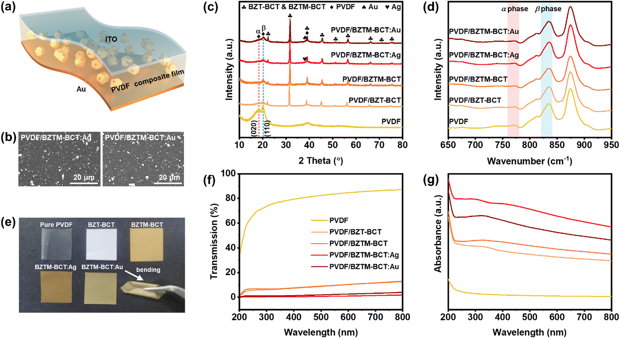 | ||
| Fig. 2 Structure and physical characterizations of PVDF composite films. (a) Schematic of the PVDF composite films. (b) SEM images for PVDF/BZTM–BCT:Au and PVDF/BZTM–BCT:Ag films. The XRD patterns (c), FTIR spectra (d), photographs (e), transmission (f) and absorbance (g) of PVDF composite films. | ||
The photographs of five PVDF composite films with different ceramic particles are given in Fig. 2e. It can be seen that the pure PVDF film is almost transparent, while its transparency is greatly reduced after introducing ceramic particles. The PVDF film with BZT–BCT particles becomes white and the PVDF films with different BZTM–BCT particles become brown, but with slightly varying brightness. After depositing the Au and Ag NPs, the stronger absorptions of the films cause their color to become darker. Additionally, the films can be greatly bent, indicating their excellent flexibility. The practical transmissions and absorbances were collected through testing UV-vis spectra (Fig. 2f and g); the results of which are consistent with the color variation of the composite films. The highest transmission but lowest absorption is observed for the pure PVDF film. On embedding the BZT–BCT and BZTM–BCT particles, the light is absorbed and scattered simultaneously by these particles. Thus, it is difficult for the light to fully pass through the composite films, resulting in largely decreasing transmission. Due to the similar content and distribution of BZT–BCT and BZTM–BCT in PVDF, the PVDF/BZT–BCT and PVDF/BZTM–BCT films show almost identical transmission. However, because the BZTM–BCT particles exhibit greater absorption than the BZT–BCT particles, the light is more absorbed but less scattered in the PVDF/BZTM–BCT than PVDF/BZT–BCT film. In addition, the scattering interface between PVDF and the ceramic particles may lead to a change in the refractive index of the film. Therefore, although the PVDF and BZT–BCT composites both exhibit almost negligible absorption in the visible light region, the PVDF/BZT–BCT composite film presents visible light absorption. After depositing Au and Ag NPs on the BZTM–BCT particles, the stronger absorption and greater scattering interface in the BZTM–BCT:Au/Ag particles cause the transmission/absorption to further decrease/increase.
Photovoltaic properties
The flexible PVDF composite film schematically demonstrated in Fig. 2a was further investigated for its photovoltaic properties. Different testing states and corresponding energy band structures are schematically described in Fig. 3a to explain the photovoltaic mechanism. The Mn-doped BZT–BCT is regarded as an n-type semiconductor due to the acceptor doping.30 Because of the work function difference between the Au (5.1 eV) and ITO (4.8 eV) electrodes,38,39 a built-in field Ebi forms in the flat films, pointing from ITO to Au electrodes. When the films are bent upward, the top surface is stretched and the bottom surface is compressed, resulting in an upward strain gradient and downward electric field Eflexo, i.e., the flexoelectric effect. An additional downward polarization field (Eps) appears upon further upward poling of the films, corresponding to the “bending + poling” samples. Eflexo and Eps have the same direction with Ebi, which leads to the energy barrier height decreasing in the ITO side, but increasing in the Au side. This change is likely to promote carrier transport and improve the photocurrent. | ||
| Fig. 3 Comparison of the photovoltaic properties of different PVDF composite films. (a) Different states of films, including flat, bending and bending after poling, as well as the corresponding energy band structures. Ebi, Eflexo and Eps represent the electric field created by Schottky barriers, flexoelectric polarization and ferroelectric polarization, respectively. The photocurrent-time curves of the five composite films under 405 nm (b)–(d) and 760 nm (e)–(g) LED light irradiation, tested for the flat samples (b) and (e), bending samples (c) and (f) and bending samples after poling (d) and (g). The light intensity is fixed at 100 mW cm−2. | ||
Fig. 3b–d presents the time-dependent photocurrents (Iph) at zero-bias under three states when illuminated with 405 nm light at 100 mW cm−2. The corresponding photocurrents are summarized in Table S1 (ESI†). For all of the samples under any state, the dark currents are pretty small at only a few pA. Under light illumination and a flat state, the pure PVDF film exhibits almost negligible Iph (about 0.07 nA). The Iph slightly increases after introducing the BZT–BCT (0.12 nA) and BZTM–BCT (0.28 nA) particles. A higher Iph for the PVDF/BZTM–BCT film compared to the PVDF/BZT–BCT film is reasonable due to its stronger photo absorption. Interestingly, depositing Ag and Au NPs on the BZTM–BCT particles causes a significant increase of the Iph in the films, reaching up to 0.82 and 1.21 nA for the PVDF/BZTM–BCT:Ag and PVDF/BZTM–BCT:Au films, respectively. These values are 3 and 4.5 times higher than that of the PVDF/BZTM–BCT film, and one order of magnitude higher than that of the pure PVDF film. This is mainly caused by the greater number of generated carriers, which will be discussed in detail in the following section.
The value for Iph is further increased on account of the flexoelectric effect, which is induced by bending the films. For the PVDF/BZTM–BCT:Au film, Iph reaches about 2.1 nA, which is 75% higher than that observed under a flat state. Furthermore, on poling the composite films and testing their Iph in the bending state, the Iph for all five films increases, while their difference becomes quite significant. For films with Au and Ag NPs, Iph is obviously higher than the others. Specifically for the PVDF/BZTM–BCT:Au film, Iph increases to about 4.0 nA, an enhancement of 86% compared to the pre-poling state. In addition, obvious and similar peak currents are observed in all composite films when the light is turned off, which is caused by the pyroelectric effect and explained in Fig. S5 (ESI†). Overall, in all of the films, Iph of the flexible PVDF-based photovoltaic device increases by 57 times through coupling the composite film preparation, flexoelectric effect and ferroelectric polarization. More importantly, the photovoltaic responses of the composite films are extended to 760 nm (Fig. 3e–g). There are no Iph for the pure PVDF film and PVDF/BZT–BCT film under the three states irradiated by 760 nm light. This is due to the narrow photo absorption range of the PVDF and BZT–BCT composites. The photovoltaic response is generated after Mn doping BZT–BCT, and is substantially improved after depositing Ag or Au NPs on the BZTM–BCT particles. Comparatively, the PVDF/BZTM–BCT:Au film exhibits a maximum photocurrent of 1.3 nA under the “poling + bending” state. The Iph changes under different states are also verified by measuring and plotting the photocurrent–voltage (I–V) curves (Fig. S6, ESI†). Whether the voltage is applied or not, the Iph increases after bending and poling. Concurrently, the open circuit voltage (Voc) slightly increases from about 0.2 V to over 0.3 V. The Iph–t curves of the upward bending samples under downward poling are presented in Fig. S7 (ESI†). In this case, Eps is in the opposite direction to Ebi and Eflexo, which weakens or even flips the downward electric field. Therefore, the photovoltaic currents almost disappear for the pure PVDF, PVDF/BZT–BCT and PVDF/BZTM–BCT films, while the PVDF/BZTM–BCT:Au and PVDF/BZTM–BCT:Ag films exhibit negative photovoltaic currents. In addition, when the light turns on/off, the pyroelectric peak current that occurs opposite to that in the upward poled samples is caused by the reverse dipole moment.
The Iph adjustability of the poled PVDF/BZTM–BCT:Au composite film was studied. Firstly, the photocurrent is nonlinearly dependent on the bending extent. Under 405 nm light illumination, the Iph increases when the distance between the two terminals decreases from 17 (flat state) to 13 mm (bending state). Meanwhile, a larger bending extent causes the effective irradiation area to significantly decrease. Thus, the Iph is decreased (Fig. 4a), which is schematically depicted in Fig. S8 (ESI†). The film exhibits a photovoltaic response in the whole visible light range, and the magnitude is almost consistent with the absorption ability to light with the corresponding wavelength (Fig. 4b). Therefore, it is reasonably believed that the composite film exhibits a photoresponse even under the illumination of near-infrared light. By contrast, the Iph of the pure PVDF film is very weak under all of the used lights (Fig. S9, ESI†).
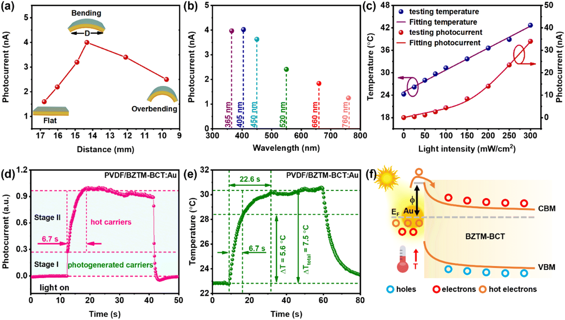 | ||
| Fig. 4 Photocurrent and photoresponse mechanism analysis of the PVDF/BZTM–BCT:Au composite film with 405 nm LED light. Photocurrent dependence on the bending extent (a), light wavelength (b) and light intensity (c). (d) Photocurrent and (e) temperature change with time. (f) Energy band structure of the Au NPs-deposited BZTM–BCT particles. | ||
Fig. 4c displays the changes in the temperature and Iph of the PVDF/BZTM–BCT:Au film with different 405 nm light intensities under the “bending + poling” state. Unlike most reported ferroelectric materials with a linear dependence of Iph on the light intensity, the Iph of the composite film increases quasi-exponentially with increasing light intensities. This phenomenon can be analyzed by eqn (2):
| Iph = Sqμ(nph + nT)E | (2) |
| nph ∝ GαP | (3) |
 | (4) |
 | (5) |
 | ||
| Fig. 5 The photocurrent changes with bending states. (a) Schematics of the flat and bending films. (b) Photocurrent evolution with the bending film under light irradiation and dark conditions. The symbols “*” and “♦” under dark condition mean that the film starts to bend and flatten, respectively. (c) Film before tip pressing and after removing tip. (d) Photocurrent corresponding to (c). | ||
Conclusions
In summary, the versatile flexible photoelectric sensors are designed by embedding the Au and Ag NPs-loaded BZTM–BCT particles into the PVDF film. The metal NPs/BZTM–BCT heterojunction is well constructed and presents excellent photo absorption in the whole visible light range. The composite particles not only make the polar β content of the film reach 93%, but also significantly enhance the photovoltaic response of PVDF from 405 nm to 760 nm. Through coupling of the composite film preparation, film bending and poling, the PVDF/BZTM–BCT:Au composite film presents an optical photocurrent that is 57 times higher than that of the pure PVDF film under 405 nm light of 100 mW cm−2. The hot carriers from Au NPs to BZTM–BCT contribute 73% of the photocurrent. Furthermore, due to its photocurrent dependence on the bending extent, the flexible photoelectric sensor can simultaneously sense photons and the movement and deformation of things. These results indicate the versatile application of the composite film.Author contributions
L. W. and Z. Y. proposed the experimental scheme. L. W. carried out the experiment. All authors analyzed and discussed the results. L. W., M. A. B. and Z. Y. edited the manuscript. All authors have given approval to the final version of the manuscript.Data availability
The data supporting this article have been included as part of the ESI.†Conflicts of interest
There are no conflicts to declare.Acknowledgements
This work was financially supported by the National Natural Science Foundation of China (Grant No. 52372130, 52202152 and 52250410356), the Natural Science Foundation of Shanghai (Grant No. 22ZR1471200), the Future Partner Special Project of the Chinese Academy of Sciences (Grant No. 030GJHZ2023076FN), the Frontier Science Key Project of the Chinese Academy of Sciences (Grant No. QYZDB-SSW-JSC027) and the Instrument Developing Project of Chinese Academy of Sciences (Grant No. ZDKYYQ20180004).Notes and references
- Y. Tang, P. Jin, Y. Wang, D. Li, Y. Chen, P. Ran, W. Fan, K. Liang, H. Ren, X. Xu, R. Wang, Y. M. Yang and B. Zhu, Nat. Commun., 2023, 14, 4961 CrossRef CAS PubMed.
- P. Rong, S. Gao, S. Ren, H. Lu, J. Yan, L. Li, M. Zhang, Y. Han, S. Jiao and J. Wang, Adv. Funct. Mater., 2023, 33, 2300159 CrossRef CAS.
- J. Lee, H. J. Kim, Y. J. Ko, J. Y. Baek, G. Shin, J. G. Jeon, J. H. Lee, J. H. Kim, J. H. Jung and T. J. Kang, Nano Energy, 2022, 97, 107178 CrossRef CAS.
- S. Cai, X. Xu, W. Yang, J. Chen and X. Fang, Adv. Mater., 2019, 31, e1808138 CrossRef PubMed.
- X. He, C. Chen, C. Li, H. Zeng and Z. Yi, Adv. Funct. Mater., 2019, 29, 1900918 CrossRef.
- T. Choi, S. Lee, Y. J. Choi, V. Kiryukhin and S.-W. Cheong, Science, 2009, 324, 63–66 CrossRef CAS PubMed.
- S. Y. Yang, J. Seidel, S. J. Byrnes, P. Shafer, C. H. Yang, M. D. Rossell, P. Yu, Y. H. Chu, J. F. Scott, J. W. AgerIII, L. W. Martin and R. Ramesh, Nat. Nanotechnol., 2010, 5, 143–147 CrossRef CAS PubMed.
- H. Liu, T. Zhao, W. Jiang, R. Jia, D. Niu, G. Qiu, L. Fan, X. Li, W. Liu, B. Chen, Y. Shi, L. Yin and B. Lu, Adv. Funct. Mater., 2015, 25, 7071–7079 CrossRef CAS.
- T. Zhao, W. Jiang, H. Liu, D. Niu, X. Li, W. Liu, X. Li, B. Chen, Y. Shi, L. Yin and B. Lu, Nanoscale, 2016, 8, 8111–8117 RSC.
- D. Zabek, J. Taylor, E. L. Boulbar and C. R. Bowen, Adv. Energy Mater., 2015, 5, 1401891 CrossRef.
- C.-M. Wu, M.-H. Chou, T. F. Chala, Y. Shimamura and R.-I. Murakami, Compos. Sci. Technol., 2019, 178, 26–32 CrossRef CAS.
- M. N. Islam, R. H. Rupom, P. R. Adhikari, Z. Demchuk, I. Popov, A. P. Sokolov, H. F. Wu, R. C. Advincula, N. Dahotre, Y. Jiang and W. Choi, Adv. Funct. Mater., 2023, 33, 2302946 CrossRef CAS.
- Z. Zhou, Q. Zhang, Z. Zhang, H. Kuang, X. Du and H. Yang, Chem. Eng. J., 2022, 442, 136241 CrossRef CAS.
- S. Nadupalli, J. Kreisel and T. Granzow, Sci. Adv., 2019, 5, eaau9199 CrossRef CAS PubMed.
- M.-M. Yang, D. J. Kim and M. Alexe, Science, 2018, 360, 904–907 CrossRef CAS PubMed.
- J. H. Haeni, P. Irvin, W. Chang, R. Uecker, P. Reiche, Y. L. Li, S. Choudhury, W. Tian, M. E. Hawley Craigo, A. K. Tagantsev, X. Q. Pan, S. K. Streiffer, L. Q. Chen, S. W. Kirchoefer, J. Levy and D. G. Schlom, Nature, 2004, 430, 758–761 CrossRef CAS PubMed.
- Y. Xia, Y. Ji, Y. Liu, L. Wu and Y. Yang, ACS Appl. Mater. Interfaces, 2022, 14, 36763–36770 CrossRef CAS PubMed.
- B. Zhang, C. Guo, X. Cao, X. Yuan, X. Li, H. Huang, S. Dong, Z. L. Wang and K. Ren, Nano Energy, 2022, 104, 107897 CrossRef CAS.
- X. Liu, F. Zhang, P. Long, T. Lu, H. Zeng, Y. Liu, R. L. Withers, Y. Li and Z. Yi, Adv. Mater., 2018, 30, 1801619 CrossRef.
- A. Biancoli, C. M. Fancher, J. L. Jones and D. Damjanovic, Nat. Mater., 2015, 14, 224–229 CrossRef CAS.
- A. Abdollahi, N. Domingo, I. Arias and G. Catalan, Nat. Commun., 2019, 10, 1266 CrossRef PubMed.
- L. Shu, S. Ke, L. Fei, W. Huang, Z. Wang, J. Gong, X. Jiang, L. Wang, F. Li, S. Lei, Z. Rao, Y. Zhou, R.-K. Zheng, X. Yao, Y. Wang, M. Stengel and G. Catalan, Nat. Mater., 2020, 19, 605 CrossRef CAS PubMed.
- Q. Huang, Z. Fan, J. Rao, T. Yang, X. Zhang, D. Chen, M. Qin, M. Zeng, X. Lu, G. Zhou, X. Gao and J. M. Liu, Adv. Electron. Mater., 2021, 8, 2100612 CrossRef.
- Y.-g Kim, H. Kim, G.-J. Lee, H.-U. Lee, S. G. Lee, C. Baek, M.-K. Lee, J.-J. Park, Q. Wang, S. B. Cho, C. K. Jeong and K.-I. Park, Nano Energy, 2021, 89, 106469 CrossRef CAS.
- R. Guo, L. You, W. Lin, A. Abdelsamie, X. Shu, G. Zhou, S. Chen, L. Liu, X. Yan, J. Wang and J. Chen, Nat. Commun., 2020, 11, 2571 CrossRef CAS PubMed.
- H. You, S. Li, Y. Fan, X. Guo, Z. Lin, R. Ding, X. Cheng, H. Zhang, T. W. B. Lo, J. Hao, Y. Zhu, H. Y. Tam, D. Lei, C. H. Lam and H. Huang, Nat. Commun., 2022, 13, 6144 CrossRef CAS PubMed.
- Y. Zhu, B. Wang, C. Deng, Y. Wang and X. Wang, Nano Energy, 2021, 83, 105801 CrossRef CAS.
- H. Liu, R. Zhu, N. Shi, L. Zhang, S. Li and J. Zhang, ACS Appl. Mater. Interfaces, 2022, 14, 55548–55558 CrossRef CAS PubMed.
- R. Su, D. Zhang, M. Wu, F.-T. Li, Y. Liu, Z. Wang, C. Xu, X. Lou, Q. Yu and Y. Yang, J. Alloys Compd., 2019, 785, 584–589 CrossRef CAS.
- L. Wang, F. Zhang, C. Chen, X. He, M. A. Boda, K. Yao and Z. Yi, Nano Energy, 2024, 119, 109081 CrossRef CAS.
- H. Li, H. Wang, X. Li, J. Huang, X. Li, S. K. Boong, H. K. Lee, J. Han and R. Guo, Nano Energy, 2022, 100, 107527 CrossRef CAS.
- M. Yan, S. Liu, Y. Liu, Z. Xiao, X. Yuan, D. Zhai, K. Zhou, Q. Wang, D. Zhang, C. Bowen and Y. Zhang, ACS Appl. Mater. Interfaces, 2022, 14, 53261–53273 CrossRef CAS PubMed.
- P. Martins, A. C. Lopes and S. Lanceros-Mendez, Prog. Polym. Sci., 2014, 39, 683–706 CrossRef CAS.
- L. Ruan, X. Yao, Y. Chang, L. Zhou, G. Qin and X. Zhang, Polymers, 2018, 10, 228 CrossRef.
- H. Z. Li, W. Z. Li, Y. J. Yang, H. L. Tai, X. S. Du, R. Y. Gao and S. Y. Li, Ceram. Int., 2018, 44, 19254–19261 CrossRef CAS.
- Y. Huan, X. Zhang, J. Song, Y. Zhao, T. Wei, G. Zhang and X. Wang, Nano Energy, 2018, 50, 62–69 CrossRef CAS.
- C. Baek, J. H. Yun, J. E. Wang, C. K. Jeong, K. J. Lee, K. I. Park and D. K. Kim, Nanoscale, 2016, 8, 17632–17638 RSC.
- H. Zhou, Q. Chen, G. Li, S. Luo, T.-B. Song, H.-S. Duan, Z. Hong, J. You, Y. Liu and Y. Yang, Science, 2014, 345, 542–546 CrossRef CAS PubMed.
- R. Zhao, N. Ma, K. Song and Y. Yang, Adv. Funct. Mater., 2019, 30, 1906232 CrossRef.
Footnote |
| † Electronic supplementary information (ESI) available. See DOI: https://doi.org/10.1039/d4mh00667d |
| This journal is © The Royal Society of Chemistry 2024 |