DOI:
10.1039/D4MH00882K
(Communication)
Mater. Horiz., 2024,
11, 5614-5621
Defect-engineering of liquid-phase exfoliated 2D semiconductors: stepwise covalent growth of electronic lateral hetero-networks†
Received
9th July 2024
, Accepted 5th September 2024
First published on 6th September 2024
Abstract
Two-dimensional (2D) in-plane heterostructures display exceptional optical and electrical properties well beyond those of their pristine components. However, they are usually produced by tedious and energy-intensive bottom-up growth approaches, not compatible with scalable solution-processing technologies. Here, we report a new stepwise microfluidic approach, based on defect engineering of liquid-phase exfoliated transition metal dichalcogenides (TMDs), to synthesize 2D hetero-networks. The healing of sulfur vacancies in MoS2 and WS2 is exploited to controllably bridge adjacent nanosheets of different chemical nature with dithiolated conjugated molecular linkers, yielding solution-processed nm-scale thick networks with enhanced percolation pathways for charge transport. In-plane growth and molecular-driven assembly synergistically lead to molecularly engineered heterojunctions suppressing the formation of tightly bound interlayer excitons that are typical of conventional TMD blends, promoting faster charge separation. Our strategy offers an unprecedented route to chemically assemble solution-processed heterostructures with functional complexity that can be further enhanced by exploiting stimuli-responsive molecular linkers.
New concepts
In this work, we have devised a solution-processed strategy based on defect-engineering to control the in-plane growth of thin hetero-networks from inks of different two-dimensional (2D) materials. To enable the formation of lateral 2D hetero-networks, π-conjugated dithiolated systems have been exploited as molecular linkers to yield MoS2–WS2 lateral heterojunctions through the healing of sulfur vacancies, mainly located at the edges of the nanosheets. The selective assembly of adjacent MoS2 and WS2 building units is guaranteed by the design of a cyclic and stepwise microfluidic process based on the sequential deposition of MoS2, π-conjugated dithiolated molecules and WS2. The synthesized covalent lateral 2D hetero-network displays distinct photophysical properties beyond those of pristine MoS2–WS2 networks, such as faster charge separation, as well as superior electrical properties than MoS2 and WS2 covalent homo-networks. Hitherto, the lack of componential selectivity and control over the edge-to-edge assembly of different 2D materials in conventional deposition techniques hindered the progress and exploration of solution-processed heterostructures. Our modular strategy paves the way toward the assembly of endless low-dimensional complex systems endowed with both tailored and uncharted characteristics.
|
Introduction
The emergence of two-dimensional (2D) materials, with their thickness down to the atomic scale, has provided access to radically new physical and chemical features.1–3 To go beyond the reach of the existing materials and unlock unprecedented paradigms in physics by pursuing functional diversification, 2D materials have been used as atomically thin building blocks to form heterojunctions endowed with tailored functionalities, either in an out-of-plane or in-plane fashion.4–6 The latter geometry enables more precise tuning of the heterostructure properties, as the lateral assembly occurs through the edges of the building units, which are more spatially separated.7 For instance, p–n nodes can be formed at the atomic scale to shrink further optoelectronic devices, beyond the current limits of Moore's law.8 Noteworthily, interfacing diverse transition metal dichalcogenides (TMDs) to form heterostructures has recently attracted much attention as it could either combine the best characteristics of their components9 or lead to enticing new physics,10,11 envisioning the development of innovative multifunctional (opto)electronic devices based on materials by design.12,13 Research on these heterostructures generally relies on physical vapor transport, chemical vapor deposition (CVD), and epitaxial growth techniques, as they offer atomic control over the assembly. Alternatively, solution processing holds promise for the scalable production of large-area architectures for printed technologies. In this context, films made by distinct 2D materials can perhaps be best defined as hetero-networks because their morphology and orientation significantly differ from conventional 2D heterostructures. However, both terms are used throughout the text.
Liquid-phase exfoliation (LPE) features high-yield, cost-effectiveness and scalability, and it outputs nanosheets dispersed in solvents of choice, being the ideal synthetic platform for large-area (opto)electronic devices compatible with printed technologies.14–16 Nevertheless, the use of LPE flakes as scaffolds for 2D lateral heterostructures is inhibited by the complete lack of control in terms of componential selectivity and preferential edge-to-edge assembly of different species arising from state-of-the art fabrication strategies, such as spin-coating, spray-coating, drop-casting, etc.17 Indeed, these techniques yield exclusively thick films of overlapped nanosheets. To eliminate this grand challenge, among the different structural defects typically existing in LPE 2D semiconducting nanostructures, chalcogen vacancies located at the edges of TMD nanosheets, which are the most abundant anomalies and conventionally considered as bottlenecks for charge transport,18–20 can be exploited as reactive sites to covalently bridge adjacent flakes to form ultrathin and continuous films through a novel supramolecular strategy.
In this work, to engineer a uniform and large-area TMD-based hetero-network displaying properties well beyond those of the individual components, dithiolated molecules are employed to covalently connect neighboring molybdenum and tungsten disulfide nanosheets (MoS2 and WS2, respectively) via microfluidic flow, which regulates the diffusion of molecules in a controlled manner.21 To ensure selective bridging, cyclic and sequential deposition of MoS2, π-conjugated dithiolated molecules and WS2 is exploited. Moreover, the use of π-conjugated molecular bidentate systems to heal sulfur vacancies in TMDs was demonstrated to be a viable strategy to generate percolation pathways, enabling efficient charge transfer among nanosheets of the same chemical nature, and thus boosting the inter-flake electronic connectivity across the interconnected network.18 It is worth noting that, compared to previous studies based on typical deposition methods such as drop-casting or spray coating,18,22 the use of a stepwise approach grants access to a larger number of sulfur vacancies in TMDs as the use of low-concentrated dispersions enables flakes to be more spatially separated, resulting in the maximization of defects healing by thiolated molecules. The synergy of multiscale microscopy and both steady-state and time-resolved spectroscopy analyses confirm that the use of such molecular bridges is critical to both control the synthesis of MoS2–WS2 lateral heterojunctions by exploiting sulfur vacancies as anchoring sites and enhance the overall electrical performance. Indeed, as revealed by photophysics investigations, faster charge separation is observed in such lateral hetero-networks compared to pristine MoS2–WS2 blends, suggesting new physical characteristics that hold potential in printed (opto)electronics. Moreover, our microfluidic approach grants access to percolation of charges at reduced thicknesses (single flake-thick). Indeed, field-effect transistors (FETs) based on solution-processed hybrid edge-bridged MoS2–WS2 heterostructures exhibit charge carrier mobilities matching state-of-the-art films made of LPE TMDs, which are typically measured in films displaying orders of magnitude higher thicknesses. The modular strategy devised in this work can be readily extended to the whole library of solution-processed low-dimensional nanomaterials, including 0D, 1D and 2D structures, and ad hoc molecular linkers with tailored multifunctional moieties, and thus serve as a powerful toolkit to assemble endless complex heterostructures with on-demand functionalities through geometrically controlled growth.
Results and discussion
Synthesis of solution-processed 2D hetero-networks through defects
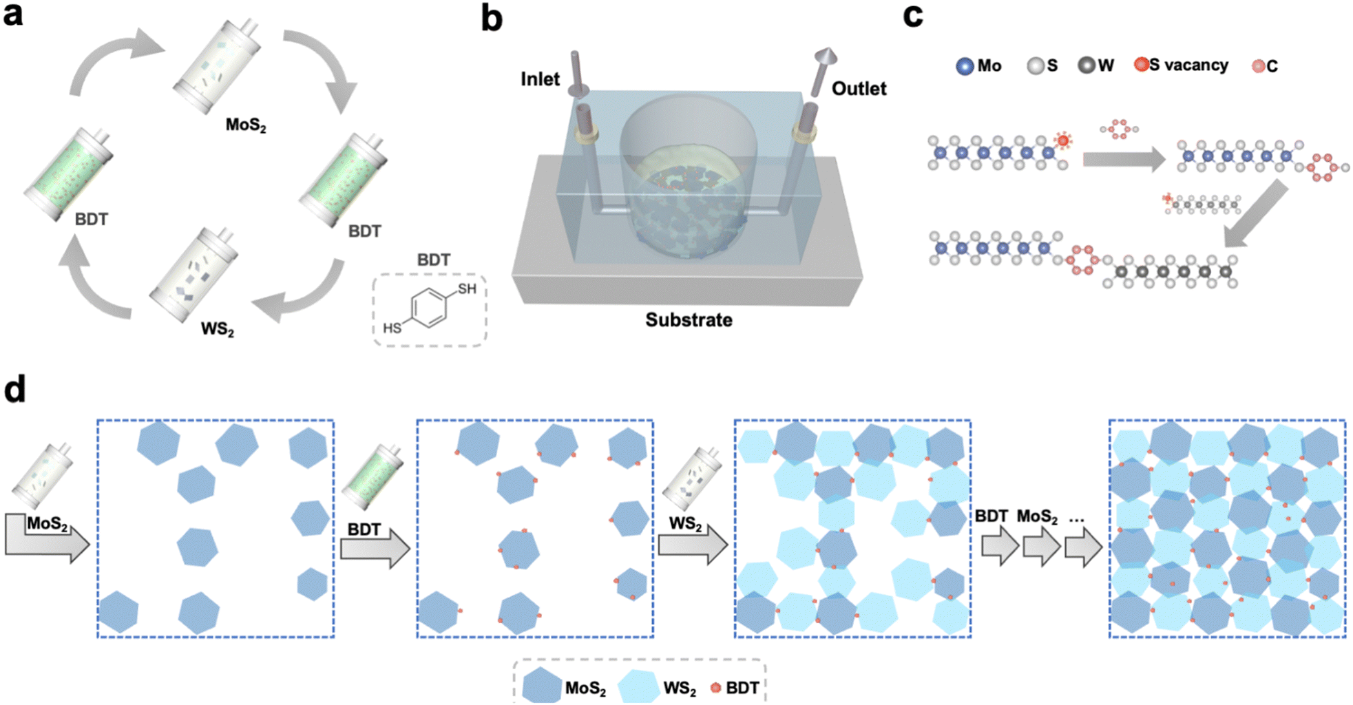
The processing steps to grow the 2D networks based on defect-engineered LPE MoS2 and WS2 are illustrated in Fig. 1. To avoid the randomness of material deposition that occurs with conventional fabrication methods (i.e. drop-casting, spin-coating, spray-coating, etc. – ESI,† Fig. S1) and maximize the amount of MoS2–WS2 heterojunctions, the synthesis of the heterostructure was carried out under laminar flow assisted by a sequential microfluidic process, using tailored conditions (Fig. S2–S4, ESI†). To demonstrate the validity of the sequential approach to grow heterostructures from solution-processed materials, a basic microfluidic system was set up. First, LPE MoS2 ink was flowing on top of a Si/SiO2 substrate, whose wettability was previously tuned via the chemisorption of a 3-(aminopropyl)triethoxysilane (APTES) monolayer to facilitate the adhesion of MoS2. Subsequently, 1,4-benzenedithiol (BDT) was used to control the in situ formation of the heterojunctions. The use of a conformationally rigid, bidentate molecule is pivotal to assemble the heterostructure. On the one hand, chalcogen vacancies exposed on the deposited MoS2 nanosheets, primarily located at the edges of 2D TMDs, act as anchoring sites for one of the two thiol-terminals of BDT. On the other hand, the second unreacted thiol end-group of the anchored BDT can be used to link covalently further nanosheets in the subsequent step. Thus, LPE WS2 ink was introduced in the microfluidic chamber to build the edge-to-edge MoS2–WS2 heterojunctions via BDT bridging. Finally, BDT was further employed to covalently functionalize the exposed sulfur vacancies at the edges of deposited WS2. The alternating steps result in a microfluidic cycle that is repeated multiple times to yield an interconnected, uniform and thin film with a coverage of ∼70% (Fig. S5, ESI†). This feasible and scalable solution-processed growth represents the first example of liquid-phase, structurally controlled, formation of an in-plane heterostructure of 2D materials, exploiting structural defects at the edges of TMDs to drive the preferentially in-plane heterojunction formation by covalently bridging the flakes of the network with dithiolated molecules. While the intrinsic conformational rigidity of the BDT molecules hinders backfolding and linkage of the two thiol end-groups to the same nanosheet, despite the control over the multiple steps of this solution-processed approach, unintentional vertical overlaps of flakes yielding homojunction formations may still occur. The morphology of the hybrid MoS2–WS2 heterostructure was investigated by scanning electron microscopy (SEM) and atomic force microscopy (AFM). To design the optimal procedure for the formation of a smooth solution-processed film, SEM analysis was used to track the nanosheets arrangement after each LPE TMD deposition step (Fig. S6, ESI†). It should be noted that the interconnected film coverage of ∼70% represents the best trade-off in terms of both heterojunction formation and thickness (Fig. 2a) as further addition of either MoS2 or WS2 nanosheets would result in a physisorption-driven 3D growth through the overlap of flakes (Fig. S7, ESI†), since the sulfur vacancies of deposited nanosheets become less accessible as a result of the dense packing of the coating. The smoothness of the thin solution-processed lateral hetero-network is further verified by AFM imaging (Fig. 2b).
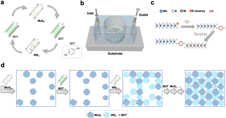 |
| | Fig. 1 Covalent hetero-network formation strategy. (a) Alternating steps of the microfluidic cycle. The process is repeated until the formation of an interconnected in-plane network. To minimize aggregation, IPA is injected between each step. (b) Schematic representation of the microfluidic setup. (c) Illustration of the healing of edge sulfur vacancies, exploited to bridge adjacent TMD flakes by BDT. (d) Schematic top-view of the stepwise growth of the lateral hetero-network, made of MoS2–BDT–WS2 core units. The last arrow illustrates that further alternating steps, following the cycle displayed in Fig. 1a, are repeated to yield the film. | |
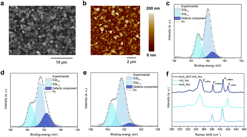 |
| | Fig. 2 Morphological and steady-state spectroscopical investigation. (a) SEM image of a film based on MoS2–WS2 heterostructure after the optimized process. (b) AFM topographical images on randomly selected areas of the heterostructure. High-resolution S 2p XPS spectrum of (c) pristine MoS2, (d) pristine WS2 and (e) hybrid MoS2–WS2 lateral hetero-network. (f) Raman spectra comparison of pristine MoS2 and WS2 with hybrid MoS2–WS2 lateral heterostructure. | |
Molecular and defect engineered MoS2–WS2 hetero-networks.
The effective in situ functionalization of both LPE MoS2 and WS2 with BDT was further assessed by X-ray photoelectron spectroscopy (XPS) and Raman spectroscopy measured in various positions over multiple samples. XPS analysis was carried out on BDT-bridged MoS2–WS2 heterostructure as well as on pristine LPE MoS2 and WS2 flakes. Notably, high-resolution S 2p spectrum of TMDs containing sulfur as chalcogen unveils the defectivity of the system, thus providing a tool for probing the healing of sulfur vacancies upon selective chemical functionalization.23,24Fig. 2c and d shows the core level S 2p spectra of pristine LPE MoS2 and WS2 films, displaying the main two S 2p3/2 and S 2p1/2 components of MoS2 (∼162.0 eV and ∼163.2 eV) and WS2 (∼162.4 eV and ∼163.6 eV), respectively. A third component for both MoS2 and WS2 at ∼161.4 eV and ∼161.7 eV, respectively, is further deconvoluted and ascribed to the defects of the crystal structure, such as the vacancy of neighboring sulfur atoms.25,26 The significant reduction of the relative area of the defects-related component in the BDT-functionalized lateral heterostructure (Fig. 2e), from 7.2 ± 1.4% and 25.3 ± 2.1% for MoS2 and WS2, respectively, to 2.8 ± 1.6%, clearly indicates the decrease of sulfur vacancies, suggesting the efficient healing through BDT covalent functionalization. In contrast, the defective component in MoS2–WS2 bi-component films without BDT treatment, displays a relative area of 9.0 ± 0.2% (Fig. S8, ESI†). Further evidence is provided by comparing the substoichiometric Mo 3d and W 4f spectra of BDT-functionalized MoS2–WS2 heterostructure and the pristine LPE MoS2–WS2 blend (Fig. S9 and S10, ESI†). The Raman spectra taken from selected locations of the lateral heterostructures are composed of an overlay of the resonance modes of both MoS2 and WS2 domains (Fig. 2f). Noteworthy, the characteristic Raman features of MoS2 and WS2 are preserved, suggesting that the interaction with BDT does not induce any apparent change to the intrinsic structural characteristics of the materials. Furthermore, the Raman mapping on the film reveals an equal distribution of both 2D components, indicating an intimate mixing of MoS2 and WS2 junctions (Fig. S11 and S12, ESI†), thus the absence of a phase segregation between the different components that would take place through a simple mixing. However, the defective presence of homojunctions cannot be fully excluded. In addition to XPS findings, the healing of sulfur vacancies by thiolated molecules is also endorsed by Raman analysis. The full width at half maximum (FWHM) of the E12g and A1g peaks of both MoS2 and WS2 witnesses a considerable reduction (as high 32.9% and 20.9% for the E12g and A1g modes of MoS2, 6.7% and 10.1% for the E12g and A1g modes of WS2, respectively. Table S1, ESI†) compared to their analogues in pristine LPE materials (Fig. 2f).27 Moreover, the spectra of the heterostructure display a considerable blue shift of the E12g and A1g Raman features (Fig. S13, ESI†), indicating the suppression of defect-induced modes, and thus being consistent with a reduction of sulfur vacancies upon BDT functionalization.28,29 The shift of the characteristic Raman bands observed in this work exceeds those observed in previous studies on defects passivation in TMDs by thiolated species,18,22 indicating a considerable increase of sulfur vacancies healing as nanosheets are more accessible by using a simple stepwise microfluidic-assisted strategy compared to typical deposition techniques that yield overlapped and stacked flakes, limiting the access to sulfur vacancies.
In situ electrochemical impedance spectroscopy.
Electrochemical impedance spectroscopy (EIS) was used to elucidate the synergistic effect of employing dithiolated molecules to propel the heterostructure development through a preferential in-plane growth and promote the creation of percolation pathways, as this technique is extremely sensitive to small variations within an electrochemical system. As illustrated in Fig. 3a, a tailored 2-electrode electrochemical cell was designed for conducting in situ EIS. The growing heterostructure onto patterned interdigitated electrodes on APTES-modified Si/SiO2 substrates acts as a barrier to the ionic conductivity (Fig. 3b), which is triggered by the application of a fixed sinusoidal voltage across the system (Fig. S14, ESI†). As the steady growth of the 2D assembly hampers the ionic conductivity between electrodes,30in situ EIS measurements exhibit a significant increase of impedance after each TMD deposition sequence (Fig. 3c), thus acting as internal gauge providing the real-time tracking of stepwise film formation via microfluidic approach. The findings indicate larger planar coverage within the interdigitating electrodes is achieved, as a result of the BDT-linking effect within adjacent flakes, propelling the favoured lateral assembly. To validate the critical role of bidentate molecules to assemble the in-plane heterostructure, EIS was performed after each MoS2 and WS2 deposition in the absence of BDT as an intermediate process. Transient impedance did not display any significant change upon TMD-loading increase, suggesting partial and uneven coverage of the surface among the interdigitating electrodes (Fig. 3d). A standard Randles equivalent circuit is used to fit the Nyquist plots (model and further discussion in ESI,† Fig. S14) and extract the charge transfer resistance (Rct),31 which is the resistance to the ionic conduction encountered at the interface between electrolyte and electrode. The architecture integrating the MoS2–WS2 heterostructure mediated by BDT witnesses a large contribution of the Rct along with the in-plane growth of the network (Fig. 3e). In contrast, the bare deposition of nanosheets without employing any molecular bridge leads to reduced Rct variation, being consistent with irregular and scarce coating of MoS2 and WS2 flakes. Typical SEM images of the film fabricated by alternating only MoS2 and WS2 nanosheets provide a distinct footprint of such EIS findings (Fig. S15, ESI†). To exclude the effect of benzene rings in the increase of Rct and further validate the in-plane growth of the heterostructure mediated by BDT, EIS has been carried out in films where thiophenols have been introduced to heal individual sulfur vacancies in MoS2 and WS2 after each deposition step, with the equivalent procedure adopted with BDT. Likewise, for the film formed by alternating MoS2 and WS2 only, thiophenol-functionalized coatings exhibit a reduced Rct comparable to the films without any molecular linker (Fig. S16, ESI†). Indeed, despite the MoS2 and WS2 functionalization through the vacancies,18 thiophenols are not able to bridge adjacent flakes due to the absence of a second thiol like in BDT, inhibiting the formation of a MoS2–WS2 network.
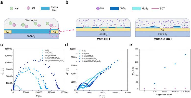 |
| | Fig. 3 Tracking the growth of heterostructures via in situ EIS. (a) Schematic illustration of the electrochemical cell used for EIS. (b) Representation of TMDs network acting as a barrier to ionic conductivity with (left) and without BDT (right). (c) Nyquist plot evolution when BDT is inserted in the microfluidic chamber between each MoS2 and WS2 step. (d) Nyquist plots after each TMD deposition step for MoS2–WS2 blends in absence of BDT. (e) Rct comparison as a function of TMD deposition for MoS2–WS2 films with and without BDT, displayed in blue and purple, respectively. | |
Photophysics of MoS2–WS2 heterostructures
As BDT enables the sequential linking of adjacent flakes, altering the overall morphology of the microfluidic-assisted grown heterostructure and regulating the distribution of its components, the impact of using such molecular linker on the overall photophysical characteristics of the synthesized MoS2–WS2 hetero-networks was revealed by transient absorption (TA) pump–probe spectroscopy studies. The TA spectra from pristine MoS2 and WS2 are dominated by their excitonic resonances: particularly the A-exciton (XA) and B-exciton (XB) from MoS2, and the XA from WS2 within the range of 550 nm to 725 nm (Fig. 4a and Fig. S17, S18, ESI†).32–34 The spectra have alternating negative and positive differential transmission (ΔT/T) signals, arising from spectral shifts and broadening of the photoexcited states relative to the ground state due to bandgap renormalization.32–35 The TA spectra of the MoS2–WS2 heterostructures are composed of signals from component materials (Fig. 4a). For the BDT-linked heterostructures, the ratio of XA (WS2): XA (MoS2) increased, indicating a higher ratio of WS2 was present in the linked heterostructures (Fig. 4b). As pump–probe delay time increased, the peaks from each of the excitons shifted spectrally, with each of the excitons in the pristine materials blue-shifting as their bandgaps returned to their ground-state values (Fig. S18–S20, ESI†). This was similar for MoS2's XA signals in the heterostructures (Fig. 4c); however, MoS2's XB and WS2's XA exhibited different trends (Fig. S19b and Fig. 4d, respectively, ESI†). For the unlinked heterostructure, the WS2's XA red-shifted with increasing pump–probe delay times – indicating further narrowing of WS2's bandgap upon formation of a long-lived interlayer exciton between MoS2 and WS2, which is typical for vertical heterostructures.36 This was not the case for the BDT-linked heterostructure: in this case, WS2's XA blue-shifted back to its ground state value in ∼100 ps, further suggesting the different architecture through the preferential in-plane growth mediated by BDT. This rapid blue shift of WS2's XA indicates the lack of formation of tightly bound interlayer excitons, indicating that the BDT-linked heterostructures promote faster charge separation. This was further evidenced by the faster relaxation dynamics of WS2's XA in the BDT-linked heterostructures compared to the unlinked heterostructures (Fig. S21 and Table S2, ESI†), suggesting potential applications in light harvesting systems.
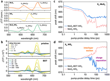 |
| | Fig. 4 Transient absorption (TA) spectra and peak shifts. (a) TA spectra of pristine MoS2, WS2, and MoS2–WS2 heterostructure averaged over pump–probe delay times of 0.1–0.3 ps. The dominant species observed within this spectral range are indicated. (b) TA spectra of MoS2–WS2 heterostructures, with or without BDT. The spectra are averaged over the pump–probe delay times listed in the legend. (c) and (d) Peak shifts for the reported species in the MoS2–WS2 heterostructures, with or without BDT, as determined from Gaussian fits to the individual peaks: (c) XA of MoS2; (d) XA of WS2. | |
Electrical characteristics
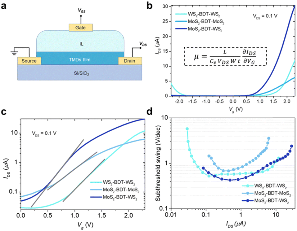
To unveil the electrical characteristics, we have fabricated proof-of-concept bottom-contact, top-gated FETs based on BDT-connected MoS2–WS2 lateral heterostructures (Fig. 5a and Fig. S24, ESI†). In this device configuration, electrolyte gating induces large carrier densities and enables strong drain-current modulation at low voltage operation.37,38 It is worth noting that the choice of an aromatic dithiolated linker over an aliphatic one to yield the covalent network of flakes is critical to grant enhanced inter-flake electronic connectivity and formation of additional percolation pathways, which go beyond the electrical features of films based on defective pristine solution-processed 2D materials.18,22 Direct comparison of the electrical performances with films exclusively made of LPE TMDs with similar thickness is not possible as their fabrication in absence of molecular linkers leads to disconnected and rough coatings, inhibiting charge transport across the device (Fig. S15, ESI†), thus exhibiting negligible transistor response. Fig. 5b displays the transfer characteristics of FET devices based on BDT-connected MoS2–WS2 lateral heterostructure as well as thin films comprising a single 2D material being either MoS2 or WS2. MoS2 and WS2 networks, also assembled via microfluidic approach, exhibit characteristic n-type and ambipolar behavior, respectively.12,38,39 As expected, the lateral heterostructure, composed of a network of alternated MoS2 and WS2 flakes connected in series by BDT, generates n-type dominated conduction, because only when both MoS2 and WS2 components are biased to be at ON state, the overall channel is turned ON. Further, the linear and symmetrical output characteristics (Fig. S25, ESI†) suggest that ohmic contact is achieved. Interestingly, the device including the hybrid MoS2–WS2 lateral heterostructure, exhibiting lower threshold voltage, shows a higher ON current, which gives rise to a higher ON/OFF current ratio. As the formation of MoS2–WS2 heterojunctions facilitates the electron conduction at the ON state, the fabricated heterostructure yields enhanced field-effect mobility (10−1 cm2 V−1 s−1), which outperform of one order of magnitude the mobility values reached by the MoS2 and WS2 networks (Table S3, ESI†). Importantly, field-effect mobilities obtained in approximately single-flake-thick films by our methodology match state-of-the-art micrometer-thick coatings based on liquid-phase exfoliated TMDs (Table S4, ESI†).16,18,22 Therefore, in-plane conductivity in the film is maximized at reduced thickness by molecularly bridging flakes through edge defects, which leads to a continuous thin network without compromising the overall thickness.
 |
| | Fig. 5 Electrical characteristics of BDT-linked TMD films. (a) Schematic illustration of the FETs. 1-Ethyl-3-methylimidazolium bis(trifluoromethanesulfonyl)imide was readily cast on top of the thin film as ionic liquid (IL). (b) Transfer curves for in-plane BDT-linked TMD films with Vg sweeping from −2.3 to +2.3 V at Vds = 0.1 V. The inset shows the equation for calculating the field-effect mobility, μ. L, channel length; Cv, volumetric capacitance; W, channel width; t, film thickness (c) subthreshold slopes obtained from logarithmic-scale current characteristics of BDT-linked TMD films. (d) Subthreshold swing as a function of IDS in films based on lateral BDT-linked TMD architectures. | |
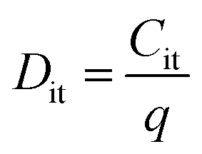
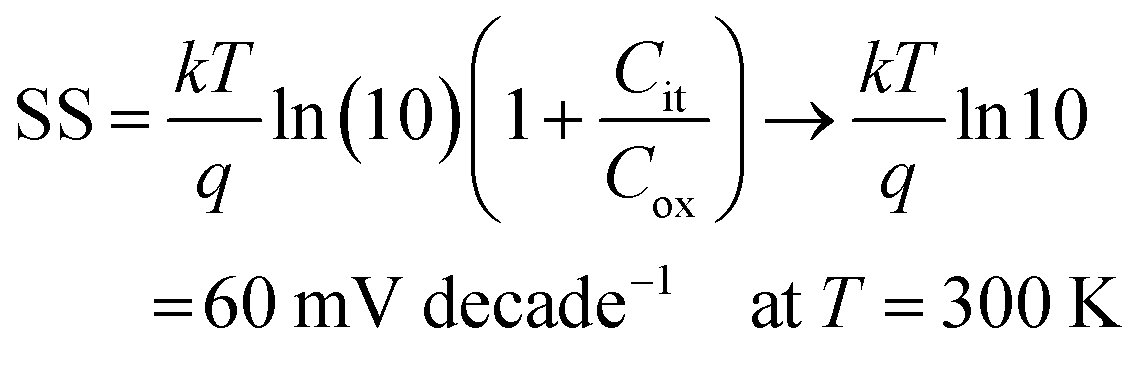
To estimate the degree of trap density into semiconducting films, the slope of transfer curves was analyzed (Fig. 5c). The steeper slope of the I–V characteristics generated by the BDT-linked MoS2–WS2 heterostructure indicates a lower amount of trap states, which we ascribe to the formation of an intimate network of heterojunctions. To quantitatively assess the trap density (Dit) of the devices, the parameter is extracted from the subthreshold swing (SS, Fig. 5d) by using the following formula:40,41
| | 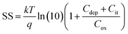 | (1) |
| |  | (2) |
where
k is the Boltzmann's constant,
T is the temperature of the measurement,
q is the electron charge,
Cox is the oxide capacitance (corresponding to the specific capacitance in IL-gated systems),
Cdep and
Cit are the depletion capacitance and the interface trap capacitance in the weak inversion region, respectively. As the effective substrate bias approaches infinity,
Cdep approaches zero. Thus, the SS can be estimated with the following approximate equation:
| |  | (3) |
The trap density
Dit in the film based on the lateral heterostructure was calculated to be 3.4 × 10
14 V
−1 cm
−2, being lower than the mono-component BDT-networks with MoS
2 and WS
2 which amount to 8.0 × 10
14 V
−1 cm
−2 and 4.4 × 10
14 V
−1 cm
−2, respectively. These results are consistent with the decrease of inter-flake trap density induced by the heterojunction formation in the synthesized MoS
2–WS
2 lateral heterostructure.
Conclusions
In summary, we have demonstrated the planar growth of solution-processed hetero-networks based on 2D TMDs by exploiting intrinsic defects via a simple sequential microfluidic approach. Sulfur vacancies in MoS2 and WS2, mainly located at the edges, have been healed by rigid, bidentate π-conjugated molecules to synergistically anchor adjacent nanosheets and promote the preferential in-plane heterostructure formation, providing percolation across the system at flake density far below state-of-the-art solution-processed films. The fabricated BDT-linked MoS2–WS2 heterostructures exhibited photophysical features that diverge from conventional blends in the absence of linkers, promoting faster charge separation. Moreover, they are endowed with superior field-effect mobility than mono-component networks due to reduced trap density resulting from the formation of heterojunctions. Our strategy to assemble heterostructures from solution-processed nanosheets can be easily extended to other classes of low-dimensional materials by making use of suitably functionalized bidentate linkers, opening up new avenues in the exploration of unprecedented optoelectronic features that go beyond the current 0D, 1D and 2D materials portfolio. Moreover, the selection of anchoring groups which selectively bind a given nanostructure and cores that can impart novel functionality to the hybrid heterostructure, thereby offering endless combinations for further integrating unprecedented solution-processed low-dimensional assemblies in miniaturized next-generation digital (opto)electronic devices.
Author contributions
A. G. R. and P. S. conceived the experiments and designed the study. A. G. K. and J. N. C. produced the raw materials. A. G. R. designed and performed the multiscale characterizations on the final functionalized materials. A. G. R. and A. Z. carried out Raman spectroscopy, XPS and impedance analysis. A. G. R. and C. M. performed electrical measurements and interpreted the data. C.E. P. and F. L. designed and performed transient absorption spectroscopy measurements and studies. All authors discussed the results and contributed to the interpretation of data. A. G. R. and P. S. co-wrote the paper with input from all co-authors. All authors have given approval to the final version of the manuscript.
Data availability
The authors confirm that the data supporting the findings of this study are available within the article and its ESI.†
Conflicts of interest
There are no conflicts to declare.
Acknowledgements
We thank Prof. Thomas Hermans for kindly providing the microfluidic cell. We acknowledge funding from the European Commission through the ERC projects SUPRA2DMAT (GA-833707) and FUTURE-PRINT (GA-694101) and the HORIZON-CL4-2023-DIGITAL-EMERGING-01-CNECT project 2D-PRINTABLE (GA-101135196) as well as the Agence Nationale de la Recherche through the Interdisciplinary Thematic Institute SysChem via the IdEx Unistra (ANR-10-IDEX-0002) within the program Investissement d’Avenir, the Foundation Jean-Marie Lehn and the Institut Universitaire de France (IUF). J. N. C. thanks Science Foundation Ireland (SFI) for support. C. E. P. acknowledges support from King Abdullah University of Science and Technology (KAUST) Global Fellowship Program under Award No. ORA-2022-5002. The authors thank Hao Mei (Shanghai Jiao Tong University) for contributing Fig. 1.
References
- Q. H. Wang, K. Kalantar-Zadeh, A. Kis, J. N. Coleman and M. S. Strano, Nat. Nanotechnol., 2012, 7, 699–712 CrossRef CAS PubMed.
- A. Rodin, M. Trushin, A. Carvalho and A. H. Castro Neto, Nat. Rev. Phys., 2020, 2, 524–537 CrossRef.
- K. S. Novoselov, A. Mishchenko, A. Carvalho and A. H. Castro Neto, Science, 2016, 353, aac9439 CrossRef CAS PubMed.
- A. G. Ricciardulli, S. Yang, J. H. Smet and M. Saliba, Nat. Mater., 2021, 20, 1325–1336 CrossRef CAS PubMed.
- E. Pomerantseva and Y. Gogotsi, Nat. Energy, 2017, 2, 1–6 Search PubMed.
- J. R. Schaibley, P. Rivera, H. Yu, K. L. Seyler, J. Yan, D. G. Mandrus, T. Taniguchi, K. Watanabe, W. Yao and X. Xu, Nat. Commun., 2016, 7, 13747 CrossRef CAS PubMed.
- M.-Y. Li, Y. Shi, C.-C. Cheng, L.-S. Lu, Y.-C. Lin, H.-L. Tang, M.-L. Tsai, C.-W. Chu, K.-H. Wei, J.-H. He, W.-H. Chang, K. Suenaga and L.-J. Li, Science, 2015, 349, 524–528 CrossRef CAS PubMed.
- X. Duan, C. Wang, J. C. Shaw, R. Cheng, Y. Chen, H. Li, X. Wu, Y. Tang, Q. Zhang, A. Pan, J. Jiang, R. Yu, Y. Huang and X. Duan, Nat. Nanotechol., 2014, 9, 1024–1030 CrossRef CAS PubMed.
- C. Huang, S. Wu, A. M. Sanchez, J. J. P. Peters, R. Beanland, J. S. Ross, P. Rivera, W. Yao, D. H. Cobden and X. Xu, Nat. Mater., 2014, 13, 1096–1101 CrossRef CAS PubMed.
- A. Pospischil, M. M. Furchi and T. Mueller, Nat. Nanotechnol., 2014, 9, 257–261 CrossRef CAS PubMed.
- J. S. Ross, P. Klement, A. M. Jones, N. J. Ghimire, J. Yan, D. G. Mandrus, T. Taniguchi, K. Watanabe, K. Kitamura, W. Yao, D. H. Cobden and X. Xu, Nat. Nanotechnol., 2014, 9, 268–272 CrossRef CAS PubMed.
- Y. Gong, J. Lin, X. Wang, G. Shi, S. Lei, Z. Lin, X. Zou, G. Ye, R. Vajtai, B. I. Yakobson, H. Terrones, M. Terrones, B. K. Tay, J. Lou, S. T. Pantelides, Z. Liu, W. Zhou and P. M. Ajayan, Nat. Mater., 2014, 13, 1135–1142 CrossRef CAS PubMed.
- Z. Zhang, Z. Huang, J. Li, D. Wang, Y. Lin, X. Yang, H. Liu, S. Liu, Y. Wang, B. Li, X. Duan and X. Duan, Nat. Nanotechnol., 2022, 17, 493–499 CrossRef CAS PubMed.
- G. Fiori, F. Bonaccorso, G. Iannaccone, T. Palacios, D. Neumaier, A. Seabaugh, S. K. Banerjee and L. Colombo, Nat. Nanotechnol., 2014, 9, 768–779 CrossRef CAS PubMed.
- R. Raccichini, A. Varzi, S. Passerini and B. Scrosati, Nat. Mater., 2015, 14, 271–279 CrossRef CAS PubMed.
- A. G. Kelly, T. Hallam, C. Backes, A. Harvey, A. S. Esmaeily, I. Godwin, J. Coelho, V. Nicolosi, J. Lauth, A. Kulkarni, S. Kinge, L. D. A. Siebbeles, G. S. Duesberg and J. N. Coleman, Science, 2017, 356, 69–73 CrossRef CAS PubMed.
- F. Bonaccorso, A. Bartolotta, J. N. Coleman and C. Backes, Adv. Mater., 2016, 28, 6136–6166 CrossRef CAS PubMed.
- S. Ippolito, A. G. Kelly, R. Furlan de Oliveira, M.-A. Stoeckel, D. Iglesias, A. Roy, C. Downing, Z. Bian, L. Lombardi, Y. A. Samad, V. Nicolosi, A. C. Ferrari, J. N. Coleman and P. Samorì, Nat. Nanotechnol., 2021, 16, 592–598 CrossRef CAS PubMed.
- H.-P. Komsa, J. Kotakoski, S. Kurasch, O. Lehtinen, U. Kaiser and A. V. Krasheninnikov, Phys. Rev. Lett., 2012, 109, 035503 CrossRef PubMed.
- S. McDonnell, R. Addou, C. Buie, R. M. Wallace and C. L. Hinkle, ACS Nano, 2014, 8, 2880–2888 CrossRef CAS PubMed.
- Y. Xia, S. Sevim, J. P. Vale, J. Seibel, D. Rodríguez-San-Miguel, D. Kim, S. Pané, T. S. Mayor, S. De Feyter and J. Puigmartí-Luis, Nat. Commun., 2022, 13, 7006 CrossRef CAS PubMed.
- S. Ippolito, F. Urban, W. Zheng, O. Mazzarisi, C. Valentini, A. G. Kelly, S. M. Gali, M. Bonn, D. Beljonne, F. Corberi, J. N. Coleman, H. I. Wang and P. Samorì, Adv. Mater., 2023, 35, 2211157 CrossRef CAS PubMed.
- Z. Lin, B. R. Carvalho, E. Kahn, R. Lv, R. Rao, H. Terrones, M. A. Pimenta and M. Terrones, 2D Mater., 2016, 3, 022002 CrossRef.
- X. Zheng, A. Calò, T. Cao, X. Liu, Z. Huang, P. M. Das, M. Drndic, E. Albisetti, F. Lavini, T.-D. Li, V. Narang, W. P. King, J. W. Harrold, M. Vittadello, C. Aruta, D. Shahrjerdi and E. Riedo, Nat. Commun., 2020, 11, 3463 CrossRef CAS PubMed.
- N. S. McIntyre, P. A. Spevack, G. Beamson and D. Briggs, Surf. Sci., 1990, 237, L390–L397 CrossRef CAS.
- M. Donarelli, F. Bisti, F. Perrozzi and L. Ottaviano, Chem. Phys. Lett., 2013, 588, 198–202 CrossRef CAS.
- S. Mignuzzi, A. J. Pollard, N. Bonini, B. Brennan, I. S. Gilmore, M. A. Pimenta, D. Richards and D. Roy, Phys. Rev. B: Condens. Matter Mater. Phys., 2015, 91, 195411 CrossRef.
- S. Bae, N. Sugiyama, T. Matsuo, H. Raebiger, K. Shudo and K. Ohno, Phys. Rev. Appl., 2017, 7, 024001 CrossRef.
- B. Chakraborty, A. Bera, D. V. S. Muthu, S. Bhowmick, U. V. Waghmare and A. K. Sood, Phys. Rev. B: Condens. Matter Mater. Phys., 2012, 85, 161403 CrossRef.
- S. Wang, J. Zhang, O. Gharbi, V. Vivier, M. Gao and M. E. Orazem, Nat. Rev. Methods Primers, 2021, 1, 1–21 CrossRef.
- E. P. Randviir and C. E. Banks, Anal. Methods, 2013, 5, 1098–1115 RSC.
- P. D. Cunningham, K. M. McCreary, A. T. Hanbicki, M. Currie, B. T. Jonker and L. M. Hayden, J. Phys. Chem. C, 2016, 120, 5819–5826 CrossRef CAS.
- S. Sim, J. Park, J.-G. Song, C. In, Y.-S. Lee, H. Kim and H. Choi, Phys. Rev. B: Condens. Matter Mater. Phys., 2013, 88, 075434 CrossRef.
- P. D. Cunningham, A. T. Hanbicki, K. M. McCreary and B. T. Jonker, ACS Nano, 2017, 11, 12601–12608 CrossRef CAS PubMed.
- E. A. A. Pogna, M. Marsili, D. De Fazio, S. Dal Conte, C. Manzoni, D. Sangalli, D. Yoon, A. Lombardo, A. C. Ferrari, A. Marini, G. Cerullo and D. Prezzi, ACS Nano, 2016, 10, 1182–1188 CrossRef CAS PubMed.
- P. Rivera, J. R. Schaibley, A. M. Jones, J. S. Ross, S. Wu, G. Aivazian, P. Klement, K. Seyler, G. Clark, N. J. Ghimire, J. Yan, D. G. Mandrus, W. Yao and X. Xu, Nat. Commun., 2015, 6, 6242 CrossRef CAS PubMed.
- S. H. Kim, K. Hong, W. Xie, K. H. Lee, S. Zhang, T. P. Lodge and C. D. Frisbie, Adv. Mater., 2013, 25, 1822–1846 CrossRef CAS PubMed.
- F. Wang, P. Stepanov, M. Gray, C. N. Lau, M. E. Itkis and R. C. Haddon, Nano Lett., 2015, 15, 5284–5288 CrossRef CAS PubMed.
- D. Braga, I. Gutiérrez Lezama, H. Berger and A. F. Morpurgo, Nano Lett., 2012, 12, 5218–5223 CrossRef CAS PubMed.
- I. Ferain, C. A. Colinge and J.-P. Colinge, Nature, 2011, 479, 310–316 CrossRef CAS PubMed.
-
S. M. Sze and K. K. Ng, 2006, Physics of Semiconductor Devices, Wiley VCH-Verlag Gmbh, 3rd edn Search PubMed.
|
| This journal is © The Royal Society of Chemistry 2024 |
Click here to see how this site uses Cookies. View our privacy policy here. 
 Open Access Article
 This Open Access Article is licensed under a
  a,
Christopher E.
Petoukhoff
b,
Anna
Zhuravlova
a,
Christopher E.
Petoukhoff
b,
Anna
Zhuravlova