
 Open Access Article
 This Open Access Article is licensed under a Creative Commons Attribution-Non Commercial 3.0 Unported Licence
Stability and photocurrent enhancement of photodetectors by using core/shell structured CsPbBr3/TiO2 quantum dots and 2D materials†
Chathurika
Maduwanthi
a,
Chao-An
Jong
b,
Waleed S.
Mohammed
c and
Shu-Han
Hsu
 *a
*a
aSchool of Integrated Science and Innovation, Sirindhorn International Institute of Technology, Thammasat University, Pathum Thani 12120, Thailand. E-mail: shuhanhsu@siit.tu.ac.th
bTaiwan Semiconductor Research Institute, National Applied Research Laboratories, Hsinchu 300091, Taiwan, ROC
cCenter of Research in Optoelectronics, Communication and Control Systems (BU-CROCCS), Bangkok University, Pathum Thani 12120, Thailand
First published on 2nd April 2024
Abstract
Ultra-stable CsPbBr3 perovskite quantum dots (QDs) were prepared, and the performance of the photodetector fabricated from them was enhanced by 2D material incorporation. This multi-component photodetector appears to have good stability in the ambient utilization environment. All inorganic CsPbBr3 QDs are potential candidates for application in photodetection devices. However, QDs have several issues such as defects on the QD surface, degradation under environmental conditions, and unfavorable carrier mobility limiting the high performance of the photodetectors. This work addresses these issues by fabricating a core/shell structure and introducing 2D materials (MXenes, Ti3C2Tx) into the device. Here, three types of photodetectors with QDs only, QDs with a core/shell structure, and QDs with a core/shell structure and MXenes are fabricated for systematic study. The CsPbBr3/TiO2 photodetector demonstrated a two times photocurrent enhancement compared to bare QDs and had good device stability after TiO2 shell coating. After introducing Ti3C2Tx into CsPbBr3/TiO2, a significant photocurrent enhancement from nanoampere (nA) to microampere (μA) was observed, revealing that MXenes can improve the photoelectric response of perovskite materials significantly. Higher photocurrent can avoid signal interference from environmental noise for better practical feasibility. This study provides a systematic understanding of the photocurrent conversion of perovskite quantum dots that is beneficial in advancing optoelectronic device integration, especially for flexible wearable device applications.
1. Introduction
In recent years, hybrid organic–inorganic perovskite materials have attracted tremendous attention, owing to their outstanding photoelectronic properties such as large absorption cross-section, long photo carrier diffusion lengths and high charge carrier mobilities.1,2 Inorganic perovskite materials are emerging with all the above superiorities while exhibiting enhanced stability compared to hybrid organic–inorganic perovskites.3 There are many studies on fully inorganic cesium-based perovskite (CsPbX3; X= Cl/Br/I) quantum dots (QD) due to their excellent optical and electrical properties.Quantum dots (QDs) are nano-sized semiconductor crystals that have garnered significant attention due to their distinctive characteristics, particularly their optical properties, leading to extensive applications in diverse fields such as solar cells, light-emitting diodes, laser technology, as well as biological and biomedical domains.4–6 The unique attributes of QDs include their small size (ranging from 4 to 12 nm in diameter), size-tunable photoluminescence (PL) emission, high extinction coefficient, elevated fluorescence quantum yield, resistance to photobleaching, and the occurrence of fluorescence intermittency.7,8 However, perovskite QDs degrade faster when exposed to moisture, oxygen, elevated temperatures, or UV light. Besides, environmental concerns are particularly significant issues in most perovskite QDs due to the presence of lead (Pb), a heavy metal.9 The research community made significant efforts to enhance the stability of perovskite by embedding QDs within a polymer matrix or inorganic salts, surface modification with waterproof capping ligands, introduction of long-chain ligands to passivate QDs, and fabrication of a core/shell structure to enhance QD stability.10,11
Among the different methods to improve the perovskite QDs' stability, metal oxide encapsulation is considered to be the most beneficial. It not only protects from environmental degradation but can also serve as an efficient photocurrent transfer path. To the best of our knowledge, only a few studies were carried out to encapsulate CsPbBr3 nanocrystals (NCs) with a titanium precursor to obtain a CsPbBr3/TiO2 core/shell structure. Z. J. Li et al. demonstrated the photostability improvement of TiO2 shell coated CsPbBr3 core/shell NCs with excellent water stability for over 12 weeks.10 H. Chen et al. demonstrated a long lifetime of CsPbBr3/TiO2 nanocrystals of about 4.04 ns of photoluminescence, and it remains stable after a period of two months in air.12 Among different phases of TiO2, the anatase phase of TiO2 demonstrates higher electron extraction properties, providing an efficient pathway to transport excited electrons from QDs. Furthermore, TiO2 can protect QDs from degradation from external factors, which is crucial for developing optoelectronic devices.13
In recent years, perovskite layer-based photodetectors (PDs) have received tremendous attention due to the perovskite's exceptional optoelectronic properties. Flexible photodetectors (FPDs), which form the core elements of flexible optoelectronic systems, play vital roles in various areas such as modern industrial production, scientific research, medical diagnosis and military defense.14 MXenes are a relatively new branch of 2D materials, which has the common formula of Mn+1XnTx (n = 1, 2 or 3). Ti3C2Tx is the most common and easily synthesized type of MXene. Tx denotes the surface functional groups such as –O, –OH, and –F which determine the exceptional properties of hydrophilic surfaces, high surface reactivity, and excellent optoelectronic properties. Ti3C2Tx is observed to be a p-type semiconductor and displays exceptional electrical conductivity, due to the diverse surface groups and the underlying metal layers.15 Recently, several researchers have reported the development of FPDs featuring perovskites/MXene heterojunctions. Pan et al. developed a simple photodetector based on the CsPbBr3/Ti3C2Tx nanocomposites, revealing that MXene can effectively facilitate the transportation of photoexcited carriers and is a promising candidate for contact materials. Furthermore, it was demonstrated that photoluminescence (PL) quenching in CsPbBr3/Ti3C2Tx indicates the presence of efficient nonradiative pathways for the integrated materials.16–18
In spite of the fact that several previous studies stated the possibility of sufficiently enhancing the photocurrent by using a TiO2 shell, there were no direct reports of photodetector devices fabricated to provide systematic validation. Hence, this work aims to develop a photodetector made of perovskite-based core/shell structure quantum dots with MXenes. This combines the advantage of TiO2 as a core/shell structure for stability improvement with 2D conductive MXene nanomaterials for efficient electron transfer to achieve higher photocurrent generation. This could have the potential to advance the field of FPDs in future applications. In order to demonstrate the improvement of the individual factors, three types of photodetectors (PDs) were fabricated: a photodetector with CsPbBr3 QDs (CsPbBr3 QD PD), photodetector with a CsPbBr3/TiO2 core/shell structure (CsPbBr3/TiO2 PD) and photodetector with a CsPbBr3/TiO2 core/shell structure with MXenes (CsPbBr3/TiO2/MXene PD). A schematic 3D view of the three PDs is shown in Fig. 1. Full material characterization was performed such as PL intensity, UV-vis absorption and photocurrent stability and enhancement after confinement of QDs by using a TiO2 layer. Furthermore, a CsPbBr3/TiO2/MXene PD was proposed and fabricated to investigate the improvement of photocurrent achieved due to efficient carrier transfer.
 | ||
| Fig. 1 Schematic 3D view of the fabricated photodetectors: (a) CsPbBr3 QD device, (b) CsPbBr3/TiO2 device and (c) CsPbBr3/TiO2/MXene device. | ||
2. Experimental
2.1 Material preparation
![[thin space (1/6-em)]](https://www.rsc.org/images/entities/char_2009.gif) :7.5. The first etching cycle took place at room temperature. In the second etching cycle, the reaction temperature was adjusted to 45 °C for the initial 6 hours, and then maintained at room temperature for the remaining time. The product solution was washed with DI water until pH reached around 5–6 and the resulting sediments were collected and dried at 70 °C for 24 hours to obtain the as-synthesized Ti3C2Tx particles for further modification. For intercalation, the as-synthesized Ti3C2Tx particles were dispersed in DMSO solvent at room temperature for 24 hours, with a ratio of 0.2 g Ti3C2Tx in 15 ml DMSO. After multiple washing cycles with DI water, the delaminated Ti3C2Tx was collected and dried at 60 °C for 24 hours.15,20
:7.5. The first etching cycle took place at room temperature. In the second etching cycle, the reaction temperature was adjusted to 45 °C for the initial 6 hours, and then maintained at room temperature for the remaining time. The product solution was washed with DI water until pH reached around 5–6 and the resulting sediments were collected and dried at 70 °C for 24 hours to obtain the as-synthesized Ti3C2Tx particles for further modification. For intercalation, the as-synthesized Ti3C2Tx particles were dispersed in DMSO solvent at room temperature for 24 hours, with a ratio of 0.2 g Ti3C2Tx in 15 ml DMSO. After multiple washing cycles with DI water, the delaminated Ti3C2Tx was collected and dried at 60 °C for 24 hours.15,20
2.2 Device fabrication
The glass substrate was cleaned using acetone. Then 30 nm/80 nm Cr/Au planar interdigitated electrodes were fabricated on the substrate by sputter deposition. The finger pattern is defined to be 200 μm in width and 200 μm in separation. Three different devices were used for the experiment: one with CsPbBr3 QDs (CsPbBr3 QDs PD), one with a CsPbBr3/TiO2 core/shell structure (CsPbBr3/TiO2 PD) and a photodetector with a CsPbBr3/TiO2 core/shell structure with MXenes (CsPbBr3/TiO2/MXene PD). A blue laser was used as an excitation source with a spot area of 12.57 mm2 that covers the whole sample. DMM6500 and SMU2450 were used to measure the corresponding current. CsPbBr3 QDs (∼10 mg) were drop cast onto the device. For the device with a core/shell structure, the sample synthesized from the same amount of QDs (∼10 mg) was drop cast, and a further 2.5 mg of MXene was introduced with the core/shell structure sample.2.3 Characterization
Transmission electron microscopy (TEM) of the QDs and the core/shell was performed using a JEM-2100 Plus with an accelerating voltage of 200 kV. Surface morphologies of photodetectors were examined using a field emission scanning electron microscope (SEM, VEGA3, TESCAN, Czech) with an acceleration voltage between 200 V and 30 kV, fitted with an EDX mapping tool (XMAX 80, OXFORD instruments). UV-vis spectra were collected using a Thermo Scientific GENESYS 10S spectrophotometer in the range from 300 nm to 700 nm, at 1 nm intervals. X-ray diffraction (XRD) (Bruker AXS model D8 Advance, Germany) was used to identify the crystal structure of QDs and core/shell structured QDs. Photoluminescence (PL) was measured by using an optical spectrometer (Compact CCD spectrometer, Thorlabs, Newton, NJ, USA) connected to a multimode glass optical fiber (Thorlabs SMA multimode fiber, M35L01). Current and time responses of the perovskite devices were recorded using a digital multimeter (Keithley DMM6500). The device was biased using a regulated DC power supply (TPR3003T-3C, 0–30 V). The current–voltage characteristics of PDs were recorded by using a source measure unit (Keithley SMU2450). A blue dot laser (λ = 450 nm, 50 mW) was used as the light source for the photovoltaic (I–V) and time response measurements.3. Results and discussion
3.1 Material characterization
The precursor solution for the synthesis of QDs was prepared by dissolving CsBr and PbBr2 in a molar ratio of 1:2. This was done with the intention of obtaining pure QDs while avoiding the formation of Cs4PbBr6.21–25 Fig. S1† shows the material characterization of QDs prepared by using a molar ratio of 1:1 of CsBr:PbBr2 (ESI†). Fig. 2(a) illustrates the crystal structure of the CsPbBr3 QDs with long ligands of OAm and OA. TBOT was selected as the Ti precursor, for coating of QDs with a TiO2 layer. The hydrolysis process facilitated the gradual deposition of a titanium matrix (TiOx) onto the surface of the QDs. Subsequently, a calcination process performed to dehydrate and remove the organic component at 400 °C, which was reported as the most suitable temperature for the calcination step without any decomposition of QDs.13
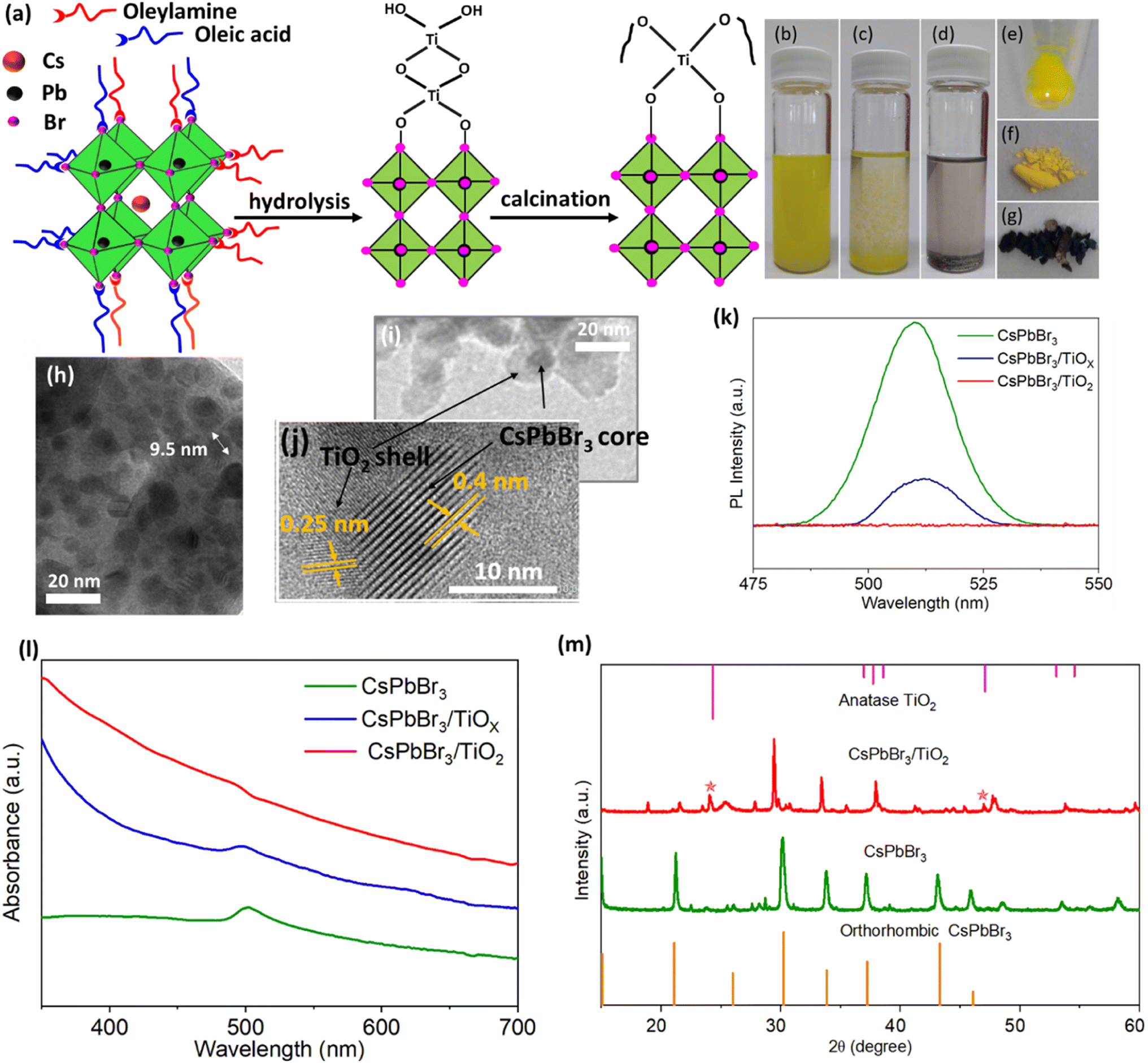 | ||
| Fig. 2 (a) Schematic illustration of coating of CsPbBr3 QDs, optical images of (b) CsPbBr3 QDs (∼1 mg ml−1), (c) CsPbBr3/TiOx and (d) CsPbBr3/TiO2 in toluene, optical images of solid state (e) CsPbBr3, (f) CsPbBr3/TiOx and (g) CsPbBr3/TiO2, TEM images of (h) CsPbBr3 QDs (i) and (j) the CsPbBr3/TiO2 – core/shell structure, (k) PL intensity, (l) UV-visible absorption spectra of CsPbBr3 QDs, CsPbBr3/TiOx and CsPbBr3/TiO2 and (m) XRD spectra of CsPbBr3 QDs and CsPbBr3/TiO2. | ||
Fig. 2(b)–(d) illustrate CsPbBr3 QDs, and QDs after the hydrolysis process and calcination process in toluene, respectively. CsPbBr3 QDs, CsPbBr3/TiOx, and CsPbBr3/TiO2 samples are shown in Fig. 2(e)–(g) in the solid state. The samples of CsPbBr3 QD after capping with TBOT still appear to be yellow. They however turn darker after calcination. This could be due to the fact that the originally obtained samples were in a powder form. Since the calcination process was carried out in an argon environment, the absence of oxygen during annealing resulted in an incomplete burning of carbon and organic residues on the surface of the CsPbBr3/TiO2 nanocrystals. This is evident from the dark appearance of the CsPbBr3/TiO2 powder after the calcination process.10
Fig. 2(h) shows the transmission electron microscopy (TEM) image of CsPbBr3 QDs with a size of 9 ± 2 nm while Fig. 2(i) illustrates the TEM image of the core–shell structure of QDs. EDS characterization of the core–shell was performed further to validate the chemical composition of quantum dots and the TiO2 structure (see ESI, Fig. S2†). Fig. 2(i) shows that CsPbBr3 QDs are wrapped with a core/shell TiO2 structure.26 Some QDs, however, are surrounded interconnectedly by TiO2. This phenomenon is attributed to the incomplete hydrolysis of high-concentration TBOT on the surface of CsPbBr3 QDs. Fig. 2(j) illustrates the lattice fringe pattern of CsPbBr3/TiO2. It depicts the 0.4 nm lattice fringe of CsPbBr3 QDs and the 0.25 nm lattice fringe of TiO2. This observation highlights the establishment of a tight interface between CsPbBr3 and TiO2.27
PL intensity was varied for CsPbBr3 QDs, CsPbBr3/TiOx, and CsPbBr3/TiO2 as shown in Fig. 2(k). The emission peak for bare QDs was 510 nm with a full width at half maximum (FWHM) of 19.7 nm. After hydrolysis, the emission intensity was reduced, and the emission peak changed to 512 nm with an FWHM of 16.4 nm. The red shift of CsPbBr3/TiOx is due to the agglomeration of the QDs bridged by the TiO2 layer. PL quenching occurred after the coating of TiO2 because the excited electrons from the conduction band of QDs under the illumination of blue laser light transfer to the layer of TiO2, which provides a new pathway for transferring electrons.10,13
UV visible absorption spectra of the CsPbBr3 QDs, CsPbBr3/TiOx and CsPbBr3/TiO2 are shown in Fig. 2(l). One can observe a sharp absorption peak at 502 nm for CsPbBr3 QDs while the absorption edge was blue shifted to 498 nm after the hydrolysis process. It is further blue shifted after the calcination process. Also, the absorption region < 400 nm was strong because of amorphous TiO2 and carbon residues after TiO2 coating.12
The X-ray diffraction (XRD) patterns of the CsPbBr3 QDs and CsPbBr3/TiO2 are shown in Fig. 2(m). The XRD pattern confirms that the crystal structure of CsPbBr3 exhibits an orthorhombic phase with identical peaks. The diffraction peaks at ∼24.0° and ∼46.9° correspond to the anatase phase of TiO2, which confirms the formation of the TiO2 layer.
3.2 Device characterization
Fig. 3(a) shows the stepwise photocurrent improvement after each modification. The device with QDs alone shows a low value of photocurrent of around 8 nA under the illumination of a blue laser (λ = 450 nm). The defects on the QD surface, long insulated ligands of OA and OAm which are used to passivate the QDs, act as barriers to the charge transport.28 This results in the QD degradation due to light, heat, and also due to humidity exposure which is a huge problem for further practical applications. Therefore, the core/shell structure is believed to increase the stability of QDs while facilitating the carrier transfer as well.10 The core/shell structure increased the photocurrent by a factor of two compared to bare QD current, which shows that yjr core–shell structure has reduced the resistance to transportation of charges when compared to QDs. Carrier recombination loss still occurred at the interface of the QDs and TiO2. This loss hinders significant current improvement.11 A CsPbBr3/TiO2/MXene PD on the other hand, shows significant photocurrent enhancement by 40000-fold compared to photocurrent generated by QDs alone at 5 V because of the new non-radiative path generated by the addition of MXenes, and excited electrons could be transferred from the conduction band (CB) of QDs–TiO2–MXene more efficiently. Therefore, a significant amount of charge carriers can be collected through the conductive MXene layer from the same amount of QDs. The spectral responsivity (R) is another vital parameter for PDs and it refers to the optical response ability of the device when excited by monochromatic light. This is related to the ability of the material to absorb photons. The spectral responsivity (R) can be defined as R = Jph/Llight, where Jph is the photocurrent and Llight is the incident-light intensity. The responsivity (R) of CsPbBr3 QDs PD, CsPbBr3/TiO2 PD and CsPbBr3/TiO2/MXene PD are calculated to be 0.1, 0.2 and 3696 A W−1 respectively, at 5 V bias. The external quantum efficiency (EQE) of each PD was calculated to be 2.9 × 10⁻¹%, 6.1 × 10⁻¹% and 1.0 × 10⁴% for CsPbBr3 QDs PD, the CsPbBr3/TiO2 PD and the CsPbBr3/TiO2/MXene PD, respectively. 3.9 × 10¹³, 6.8 × 10¹² and 7.6 × 10¹⁴ jones were the detectivity of the CsPbBr3 QDs PD, CsPbBr3/TiO2 PD and CsPbBr3/TiO2/MXene PD, respectively.29–31 All measurements were carried out at 81 W m−2 power density of the incident laser. This confirmed that utilizing the core/shell structure and introducing MXenes enhanced the photovoltaic performance of the PDs (see ESI, Table S1†). Note that a ratio Ion/Ioff = 1.7 for the CsPbBr3/TiO2/MXene PD was observed at 5 V bias. The positive photocurrent spikes are evidence for the existence of accumulated photoexcited holes in interfaces within electrodes under the illumination of a laser.32,33 It is also found that stable photocurrent measured for the core–shell structure of QDs, can be effectively switched on and off with very good repeatability for 1000 seconds as illustrated in Fig. 3(b). Consistent switching behavior was also observed for the device after six weeks of storage in a nitrogen box (see ESI, Fig. S3†). Fig. 3(c) shows the non-radiative electron flow of the excited electrons from the CB of QDs, and the energy levels of each material used in the CsPbBr3/TiO2/MXene PD.
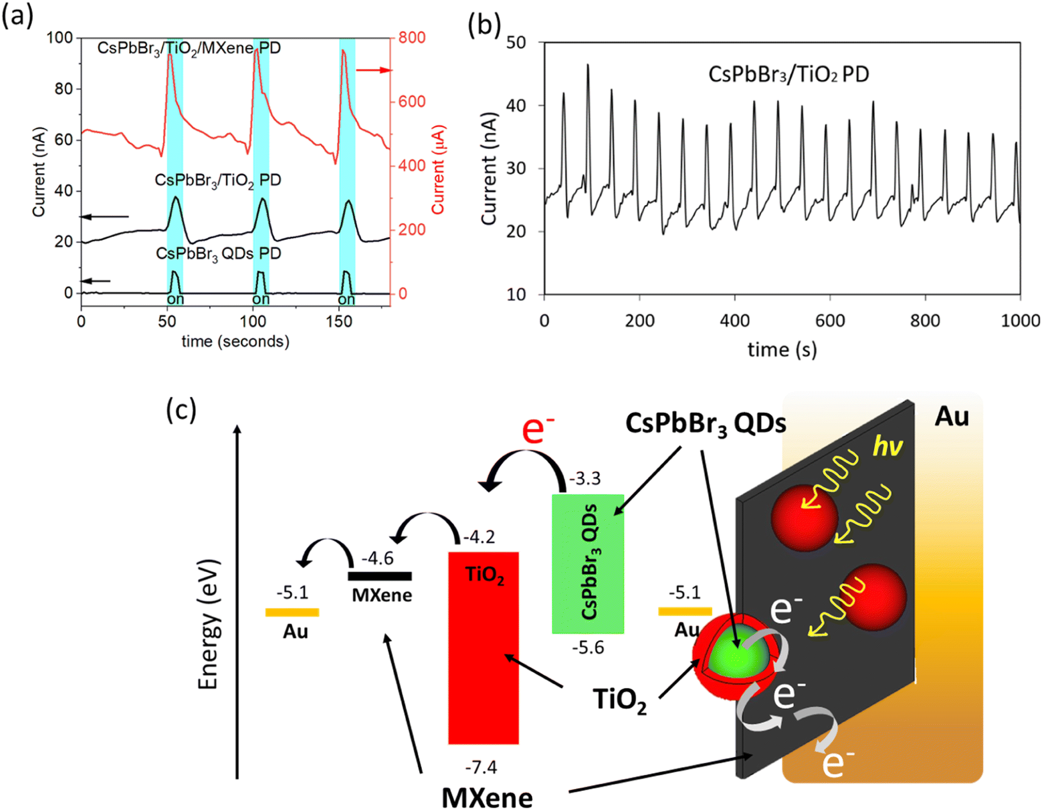 | ||
| Fig. 3 (a) Photocurrent–time response measured in the dark and under the illumination of a blue laser with 5 V bias of three photodetectors, (b) photocurrent–time response of the CsPbBr3/TiO2 photodetector measured in the dark and under illumination of a blue laser with a 16 min alternative pulse, and (c) energy level diagram of the CsPbBr3/TiO2/MXene photodetector. | ||
Fig. 4(a) shows the I–V response of the CsPbBr3 QD PD and CsPbBr3/TiO2/MXene PD in the dark and under illumination. There is no current observed as dark current for QDs while conductive MXenes shows μA range dark current. Higher dark current for the CsPbBr3/TiO2/MXene PD could be mainly due to the presence of a conductive MXene in the device. SEM images of the CsPbBr3/TiO2 PD and CsPbBr3/TiO2/MXene PD are shown in Fig. 4(b) and (c) respectively. The EDX characterization of CsPbBr3/TiO2 PD and CsPbBr3/TiO2/MXene PD can be found in the ESI (Fig. S4 and S5†). Fig. 4(d) and (e) show the optical image of the CsPbBr3/TiO2/MXene PD and the dimensions of the Au electrode. Prior study also observed the increase in the current density of the core/shell structure using CsPbBr3 and CsPbBr3/TiO2 NCs as reference electrodes to the normal hydrogen electrode (NHE).10 This is consistent with the finding when such a core/shell structure was used to fabricate a FPD device and the performance was further enhanced by introducing the 2D materials, where the flake structure of MXenes provides conformal contact with QD. In addition, many studies have been reported on photoconductive devices based on varied configurations and material morphologies, including nanoparticles and nanosheets of CsPbBr3 perovskites. Some of them exhibit good performances regarding responsivity, rise time, and detectivity, as shown in Table 1. The as-fabricated device of the CsPbBr3/TiO2/MXene PD shows the highest responsivity and detectivity.
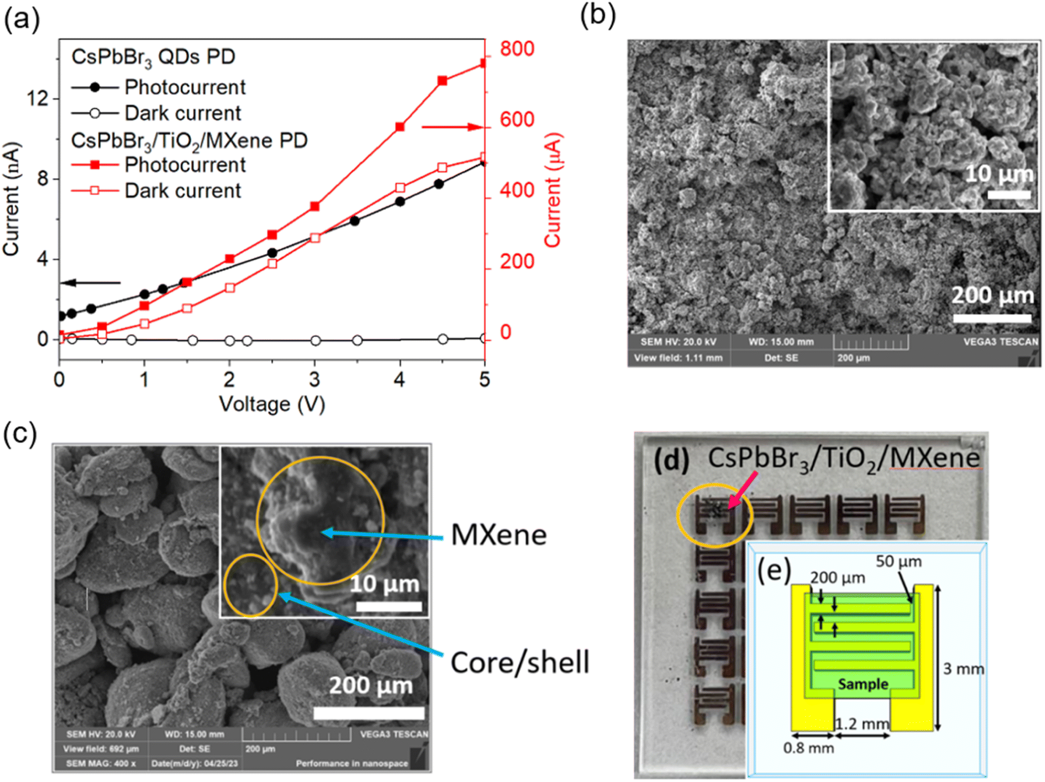 | ||
| Fig. 4 (a) I–V curve of the CsPbBr3 QD PD and CsPbBr3/TiO2/MXene PD in the dark and under illumination of a blue laser, SEM images of the (b) CsPbBr3/TiO2 PD and (c) CsPbBr3/TiO2/MXene PD, (d) optical image of the CsPbBr3/TiO2/MXene PD and (e) schematic 2D view of the measurements of Au interdigitated electrodes with the sample. | ||
| Configuration | Material structure | Response time | Responsivity (R) (A W−1) | Irradiation power density | Detectivity (jones) | Ref. |
|---|---|---|---|---|---|---|
| Au/CsPbBr3 (Au NCs)/Au | Nanoparticles | 1.2 ms | 0.01 | 46.5 W m−2 | 4.5 × 10⁸ | 34 |
| Au/CsPbBr3 (mp-TiO2)/Au | Nanoparticles | 9 s | 3.5 (4 V) | NA (150 W lamp) | NA | 35 |
| Au/CsPbBr3–MPA (mp-TiO2)/Au | Nanoparticles | 4.7 s | 24.5 | 1 W m−2 (λ = 405 nm) | 8.9 × 10¹³ | 36 |
| CsPbBr3/PbSe | Nanoparticles | NA | 7.17 (5 V) | 0.25 W m−2 (λ = 365 nm) | 9.0 × 10¹² | 37 |
| CsPbBr3 | Thin film | NA | 0.12 | 4.7 W m−2 | NA | 38 |
| CsPbBr3 | Nanosheet | NA | 0.09 (3 V) | (λ = 265 nm) | 4.1 × 10¹¹ | 39 |
| CsPbBr3 QDs PD | Nanoparticles | 2.63 s | 0.10 (5 V) | 81 W m−2 (λ = 450 nm) | 3.9 × 10¹³ | This work |
| CsPbBr3/TiO2 PD | Nanoparticles | 3.63 s | 0.20 (5 V) | 81 W m−2 (λ = 450 nm) | 6.8 × 10¹² | This work |
| CsPbBr3/TiO2/MXene PD | Nanoparticles | 2.59 s | 3696 (5 V) | 81 W m−2 (λ = 450 nm) | 7.6 × 10¹⁴ | This work |
4. Conclusion
In summary, three types of PDs were fabricated to demonstrate the performance systematically: CsPbBr3 QD PD, CsPbBr3 QDs/TiO2 PD and CsPbBr3/TiO2/MXene PD. The device with the CsPbBr3 QDs/TiO2 PD appears to improve the stability and allows efficient photoinduced charge transfer through TiO2. Consistent performance was observed upon nearly twenty minutes of exposure. The CsPbBr3/TiO2 PD was observed to enhance the photocurrent twice compared to a PD with pristine QDs. Ultimately, the CsPbBr3/TiO2/MXene PD improved the photocurrent significantly, which was 40000 times more than that of the device with pristine QDs. This can be attributed to the effective electron transfer from QDs to MXenes upon photoirradiation. This QD decorated multilayer MXene was interconnected, which forms a conductive path to the interdigitated electrode, which sufficiently reduces the current loss. This work will lead to promising applications in integrated optoelectronic devices such as FPDs. Moreover, other conductive materials can be further introduced, such as conducting polymers, as flexible matrices for better multicomponent blending. This can address the possible issue of the current drop casting method, where a possible gap or spacing exists among multiple components.
Author contributions
C. Maduwanthi: original draft; S.-H. Hsu: draft review and funding; C.-A. Jong: funding; W. S. Mohammed: supervision.Conflicts of interest
There are no conflicts to declare.Acknowledgements
This work was supported by the Thailand Science Research and Innovation Fundamental Fund fiscal year 2024 and NARLabs I-Dream International Cooperation Project (13111F1201). The authors gratefully acknowledge the support from the School of Integrated Science and Innovation (ISI), the Center of Excellence in Functional Advanced Materials Engineering (CoE FAME), the Sirindhorn International Institute of Technology (SIIT), Thammasat University and the Taiwan Semiconductor Research Institute (TSRI).References
- Y. Wang, L. Song, Y. Chen and W. Huang, Emerging New-Generation Photodetectors Based on Low-Dimensional Halide Perovskites, ACS Photonics, 2020, 7(1), 10–28, DOI:10.1021/acsphotonics.9b01233.
- Y. Wang, Y. Zhang and Y. Lu, et al., Hybrid Graphene-Perovskite Phototransistors with Ultrahigh Responsivity and Gain, Adv. Opt. Mater., 2015, 3(10), 1389–1396, DOI:10.1002/adom.201500150.
- Y. Dong, Y. Gu and Y. Zou, et al., Improving All-Inorganic Perovskite Photodetectors by Preferred Orientation and Plasmonic Effect, Small, 2016, 12(40), 5622–5632, DOI:10.1002/smll.201602366.
- L. X. Wang, C. G. Tang and Z. S. Tan, et al., Double-type-I charge-injection heterostructure for quantum-dot light-emitting diodes, Mater. Horiz., 2022, 9(8), 2147–2159, 10.1039/d1mh00859e.
- Y. Rui, Z. Jin and X. Fan, et al., Defect passivation and electrical conductivity enhancement in perovskite solar cells using functionalized graphene quantum dots, Mater. Futures, 2022, 1(4), 045101, DOI:10.1088/2752-5724/ac9707.
- H. Yang, S. Li and L. Zhang, et al., Observation of high-density multi-excitons in medium-size CdSe/CdZnS/ZnS colloidal quantum dots through transient spectroscopy and their optical gain properties, Nanoscale, 2022, 14(14), 5369–5376, 10.1039/D2NR00761D.
- B. Gidwani, V. Sahu and S. S. Shukla, et al., Quantum dots: prospectives, toxicity, advances and applications, J. Drug Delivery Sci. Technol., 2021, 61, 102308, DOI:10.1016/j.jddst.2020.102308.
- S. Kargozar, S. J. Hoseini, P. B. Milan, S. Hooshmand, H. W. Kim and M. Mozafari, Quantum Dots: A Review from Concept to Clinic, Biotechnol. J., 2020, 15(12), 2000117, DOI:10.1002/biot.202000117.
- M. Wang, W. Wang and B. Ma, et al., Lead-Free Perovskite Materials for Solar Cells, Nano-Micro Lett., 2021, 13(1), 62, DOI:10.1007/s40820-020-00578-z.
- Z. J. Li, E. Hofman and J. Li, et al., Photoelectrochemically active and environmentally stable cspbbr3/tio2 core/shell nanocrystals, Adv. Funct. Mater., 2018, 28(1), 1704288, DOI:10.1002/adfm.201704288.
- B. Z. Zhou, M. J. Liu, Y. W. Wen, Y. Li and R. Chen, Atomic layer deposition for quantum dots based devices, Opto-Electron. Adv., 2020, 3(9), 1–14, DOI:10.29026/oea.2020.190043.
- H. Chen, R. Li, A. Guo and Y. Xia, Highly fluorescent CsPbBr3/TiO2 core/shell perovskite nanocrystals with excellent stability, SN Appl. Sci., 2021, 3(6), 654, DOI:10.1007/s42452-021-04648-8.
- P. Nuket, T. Kida and P. Vas-Umnuay, Influence of Annealing Temperature on Structural Properties and Stability of CsPbBr3/TiO2Core/Shell, in IOP Conference Series: Materials Science and Engineering, IOP Publishing Ltd, 2020, vol 965, DOI:10.1088/1757-899X/965/1/012023.
- X. Zhang, X. Liu and Y. Huang, et al., Review on flexible perovskite photodetector: processing and applications, Front. Mech. Eng., 2023, 18(2), 33, DOI:10.1007/s11465-023-0749-z.
- L. C. T. Cao, M. H. Zhou and P. Opaprakasit, et al., Facile Fabrication of Oxygen-Enriched MXene-Based Sensor and Their Ammonia Gas-Sensing Enhancement, Adv. Mater. Interfaces, 2023, 10(16), 2300166, DOI:10.1002/admi.202300166.
- H. Xu, A. Ren, J. Wu and Z. Wang, Recent Advances in 2D MXenes for Photodetection, Adv. Funct. Mater., 2020, 30(24), 2000907, DOI:10.1002/adfm.202000907.
- A. Pan, X. Ma and S. Huang, et al., CsPbBr3 Perovskite Nanocrystal Grown on MXene Nanosheets for Enhanced Photoelectric Detection and Photocatalytic CO2 Reduction, J. Phys. Chem. Lett., 2019, 10(21), 6590–6597, DOI:10.1021/acs.jpclett.9b02605.
- H. Li, Z. Li and S. Liu, et al., High performance hybrid MXene nanosheet/CsPbBr3 quantum dot photodetectors with an excellent stability, J. Alloys Compd., 2022, 895, 162570, DOI:10.1016/j.jallcom.2021.162570.
- Y. Xie, Y. Yu and J. Gong, et al., Encapsulated room-temperature synthesized CsPbX 3 perovskite quantum dots with high stability and wide color gamut for display, Opt. Mater. Express, 2018, 8(11), 3494, DOI:10.1364/ome.8.003494.
- L. C. T. Cao, C. A. Jong, S. H. Hsu and S. F. Tseng, A Simple Approach to MXene Micropatterning from Molecularly Driven Assembly, ACS Omega, 2021, 6(51), 35866–35875, DOI:10.1021/acsomega.1c06662.
- Y. Xie, Y. Yu and J. Gong, et al., Encapsulated room-temperature synthesized CsPbX 3 perovskite quantum dots with high stability and wide color gamut for display, Opt. Mater. Express, 2018, 8(11), 3494, DOI:10.1364/ome.8.003494.
- M. F. Leitão, M. S. Islim and L. Yin, et al., Pump-power-dependence of a CsPbBr 3 -in-Cs 4 PbBr 6 quantum dot color converter, Opt. Mater. Express, 2019, 9(8), 3504, DOI:10.1364/ome.9.003504.
- L. Wang, H. Liu, Y. Zhang and O. F. Mohammed, Photoluminescence Origin of Zero-Dimensional Cs4PbBr6 Perovskite, ACS Energy Lett., 2020, 5(1), 87–99, DOI:10.1021/acsenergylett.9b02275.
- Q. A. Akkerman, S. Park and E. Radicchi, et al., Nearly Monodisperse Insulator Cs4PbX6 (X = Cl, Br, I) Nanocrystals, Their Mixed Halide Compositions, and Their Transformation into CsPbX3 Nanocrystals, Nano Lett., 2017, 17(3), 1924–1930, DOI:10.1021/acs.nanolett.6b05262.
- M. Chen, Y. Yuan, Y. Liu, D. Cao and C. Xu, High-quality all-inorganic CsPbBr3 single crystals prepared by a facile one-step solution growth method, RSC Adv., 2022, 12(23), 14838–14843, 10.1039/d2ra01900k.
- J. Hao, G. Tai, J. Zhou, R. Wang, C. Hou and W. Guo, Crystalline Semiconductor Boron Quantum Dots, ACS Appl. Mater. Interfaces, 2020, 12(15), 17669–17675, DOI:10.1021/acsami.9b19648.
- W. Shao, G. Tai, C. Hou, Z. Wu, Z. Wu and X. Liang, Borophene-Functionalized Magnetic Nanoparticles: Synthesis and Memory Device Application, ACS Appl. Electron. Mater., 2021, 3(3), 1133–1141, DOI:10.1021/acsaelm.0c01004.
- K. Chen, X. Zhang and P. A. Chen, et al., Solution-Processed CsPbBr3 Quantum Dots/Organic Semiconductor Planar Heterojunctions for High-Performance Photodetectors, Advanced Science, 2022, 9(12), 2105856, DOI:10.1002/advs.202105856.
- Z. Wu, G. Tai and R. Liu, et al., Van der Waals Epitaxial Growth of Borophene on a Mica Substrate toward a High-Performance Photodetector, ACS Appl. Mater. Interfaces, 2021, 13(27), 31808–31815, DOI:10.1021/acsami.1c03146.
- Y. Zhang, F. Wang and X. Zhao, et al., 2D Ruddlesden–Popper perovskite sensitized SnP 2 S 6 ultraviolet photodetector enabling high responsivity and fast speed, Nanoscale Horiz., 2023, 8(1), 108–117, 10.1039/D2NH00466F.
- G. Tai, B. Liu, C. Hou, Z. Wu and X. Liang, Ultraviolet photodetector based on p-borophene/n-ZnO heterojunction, Nanotechnology, 2021, 32(50), 505606, DOI:10.1088/1361-6528/ac27db.
- M. Wang, F. Ren and J. Zhou, et al., N Doping to ZnO Nanorods for Photoelectrochemical Water Splitting under Visible Light: Engineered Impurity Distribution and Terraced Band Structure, Sci. Rep., 2015, 5, 12925, DOI:10.1038/srep12925.
- A. G. Tamirat, A. A. Dubale, W. N. Su, H. M. Chen and B. J. Hwang, Sequentially surface modified hematite enables lower applied bias photoelectrochemical water splitting, Phys. Chem. Chem. Phys., 2017, 19(31), 20881–20890, 10.1039/c7cp02890c.
- Y. Dong, Y. Gu and Y. Zou, et al., Improving All-Inorganic Perovskite Photodetectors by Preferred Orientation and Plasmonic Effect, Small, 2016, 12(40), 5622–5632, DOI:10.1002/smll.201602366.
- L. Zhou, K. Yu and F. Yang, et al., All-inorganic perovskite quantum dot/mesoporous TiO2 composite-based photodetectors with enhanced performance, Dalton Trans., 2017, 46(6), 1766–1769, 10.1039/c6dt04758k.
- L. Zhou, K. Yu and F. Yang, et al., Insight into the effect of ligand-exchange on colloidal CsPbBr3 perovskite quantum dot/mesoporous-TiO2 composite-based photodetectors: much faster electron injection, J. Mater. Chem. C, 2017, 5(25), 6224–6233, 10.1039/C7TC01611E.
- J. Hu, S. Yang and Z. Zhang, et al., Solution-processed, flexible and broadband photodetector based on CsPbBr3/PbSe quantum dot heterostructures, J. Mater. Sci. Technol., 2021, 68, 216–226, DOI:10.1016/j.jmst.2020.06.047.
- D. B. Kim, J. Han and Y. S. Jung, et al., Origin of the anisotropic-strain-driven photoresponse enhancement in inorganic halide-based self-powered flexible photodetectors, Mater. Horiz., 2022, 9(4), 1207–1215, 10.1039/D1MH02055B.
- C. Y. Wu, Y. X. Le and L. Y. Liang, et al., Non-ultrawide bandgap CsPbBr3 nanosheet for sensitive deep ultraviolet photodetection, J. Mater. Sci. Technol., 2023, 159, 251–257, DOI:10.1016/j.jmst.2023.03.032.
Footnote |
| † Electronic supplementary information (ESI) available. See DOI: https://doi.org/10.1039/d3na01129a |
| This journal is © The Royal Society of Chemistry 2024 |