DOI:
10.1039/D4NA00598H
(Paper)
Nanoscale Adv., 2024,
6, 6253-6264
Optical, magnetic, and transport properties of two-dimensional III-nitride semiconductors (AlN, GaN, and InN) due to acoustic phonon scattering
Received
22nd July 2024
, Accepted 27th September 2024
First published on 4th October 2024
Abstract
In this paper, the magneto-optical transport (MOT) properties of III-nitride Pöschl–Teller quantum well (QW) semiconductors, including AlN, GaN, and InN, resulting from the acoustic phonon interaction are thoroughly investigated and compared by applying the technique of operator projection. In particular, a comparison is made between the Pöschl–Teller QW results and the square QW ones. The findings demonstrate that the MOT properties of III-nitride QW semiconductors resulting from acoustic phonon scattering are strongly influenced by the quantum system (QS) temperature, applied magnetic field, and QW width. When the applied magnetic field and QS temperature increase, the absorbing FWHM in AlN, GaN, and InN increases; on the other hand, it diminishes when the QW's width increases. The absorbing FWHM in GaN is smaller and varies slower compared with AlN; inversely, it is larger and varies faster compared with InN. In other words, the absorbing FWHM in AlN is the largest and the smallest in InN. Compared to the square QW in AlN, GaN, and InN, the absorbing FWHMs in the Pöschl–Teller QW vary more quickly and have greater values. The absorbing FWHMs resulting from the acoustic phonon interaction in III-nitrides are strongly dependent on the nanostructure's geometric shape and parameters. Our findings provide useful information for the development of electronic devices.
1 Introduction
Aluminum nitride (AlN), indium nitride (InN), and gallium nitride (GaN), along with their associated alloys (their ternary compounds), form a group of materials known as “III-nitrides”. This special branch of the III–V compound semiconductors has significantly revolutionized the lighting industry, as a result of the high brightness, flexibility, and efficiency of short wavelength III-nitride light emitting diodes (LEDs) and laser diodes (LDs), enabling significant cost and energy reductions (savings) on a hitherto unheard scale. The capacity of III-nitride LEDs to emit light efficiently and brightly in the blue to UV spectral region is a significant advancement in lighting. Without these capabilities, producing white light LEDs would be very challenging.1 Since the blue LED's high brightness was first demonstrated, III-nitride semiconductors have had a remarkable impact on the world. The growing use of LEDs to replace conventional lighting fixtures like incandescent light-bulbs is evidence of this. The III-nitride semiconductor group, including AlN, GaN, and InN, is essential for enabling compact and highly efficient great power applications. Three various crystal structure shapes can be formed by III nitride (AlN, GaN, and InN) semiconductors. These include hexagonal wurtzite, zinc blende and rock salt, and two cubic structures. The main focus of research and industry is on the thermodynamically stable wurtzite.2 Moreover, we introduce the important properties of wurtzite III-nitride lattices as follows: III-nitride semiconductors with hexagonal lattices have been a focal point of thorough investigations within the industrial and academic realms owing to their superior structural stability even under ambient conditions. Additionally, there has been a notable resurgence of interest in the exploration of cubic III-nitrides, particularly in the context of their potential applications in LED technology.3 The III-nitride-based LEDs in the blue-to-yellow region have been successfully commercialised, along with the development of ultraviolet detectors and injection lasers. These outcomes led to a shift in basic studies' focus on semiconductors with a wide direct bandgap range, specifically to comprehend their optical characteristics.4 However, their advantageous characteristics for the development of high-frequency transistors, electronic power devices, and high performance,5 as well as their better properties compared to silicon-based materials, were quickly recognised. The attempts to study the III-nitrides’ steady-state transport characteristics, aimed at improving the determination of parameters of the band structure and bulk material,6 are crucial for confidently establishing their value in electronic devices.7 The III-nitrides can have two different types, depending on how the first layer is placed on the surface during growth. This happens because there is no symmetry in the plane. The III-nitride (AlN, GaN, and InN) semiconductors with a wurtzite crystal structure are considered polar materials due to their intrinsic polarity, meaning they possess spontaneous polarization even in the absence of an external electric field. The reason why III-nitrides are so interesting for optoelectronic applications stems from the ability to achieve a wide direct band-gap range through the process of alloying. In addition, III-nitride materials have garnered significant interest for optoelectronic applications due to their potential to absorb and emit light in infrared and ultraviolet regions, and across the entire visible spectrum. The III-nitrides' wide direct band-gap range is a crucial characteristic of their use in photonic devices. This property enables efficient photon absorption as well as photon emission without requiring phonon interaction, which is critical for the performance of these devices, as shown in ref. 1. However, several early studies8 demonstrated that the III-nitrides' electronic band structures play a crucial role in determining their optical characteristics. The non-uniform arrangement of atoms in the lattice leads to a perturbation of the periodic potential that acts on the crystal's electrons as they deviate from their equilibrium positions. This perturbation results in an energy associated with the electron–phonon (e–p) interaction. Various types of interactions exist, such as the Fröhlich interaction involving LO-phonons, the interaction based on deformation potential with both the optical phonons and the acoustic phonons, and the interaction due to piezoelectric effects involving acoustic phonons. These interactions occur because of the different ways in which the vibrations of the lattice disturb the movements of electrons. They greatly affect the III-nitride semiconductors' optical and magnetic characteristics resulting from the ionic properties of III-nitrides. It is known that a better understanding of electron–phonon interaction is crucial for optimizing device functionality and performance. Therefore, we perform a comparative study of the optical, transport, and magnetic characteristics of two-dimensional III-nitride semiconductors due to acoustic phonon interaction, aimed at as follows: understanding the contribution of acoustic phonons to electron–phonon scattering mechanisms in III-nitride semiconductors which is significant and cannot be ignored, demonstrating that the magneto-optical properties of AlN, GaN, and InN have considerable differences, providing scientific insights that help orient the experimental efforts into device design and fabrication and a better understanding of the advantages of the operator projection method. The benefits of applying this approach are all quantum transition processes in two-dimensional III-nitride (specifically AlN, GaN, and InN) semiconductors can be easily analysed; the final analytical formulae of the conductivity tensor (CT), absorbing power (AP), and line-shape function of magneto-optical (MO) transitions are obtained to be very obvious; the experimental measurements of the absorbed spectrum width of the MO transitions are closely related to the MOCT and its line-shape function. On the other hand, the MO transitions are characterized as follows: electronic states undergo quantization in the low-dimensional III-nitride heterostructures (specifically AlN, GaN, and InN) when a B (static magnetic field) is present along the z-axis. At the same time, if AlN, GaN, and InN QW semiconductors are exposed to an electromagnetic wave, then for one, the electrons in these low dimensional III-nitride heterostructures will cause MO transport in which the most prevalent one is the cyclotron one through absorbing an appropriate photon energy. On the other hand, our focus, in this study, is on the AP of MO transitions and the FWHMs. The reason behind this is that the absorbing FWHM regarding the acoustic phonon scattering in low-dimensional III-nitride heterostructures is highly sensitive to the various mechanisms of electron scattering, wherefore, the behavior of electrons in the above-III-nitride heterostructures is heavily influenced by scattering mechanisms. As a result, researching MO transitions in two-dimensional III-nitride heterostructures is valuable for gaining insights into the electronic structure in AlN, GaN, and InN semiconductors. In recent years, the e–p interaction in Q2D III-nitride heterostructures has been researched in several studies,8–13 where the authors have demonstrated that the e–p interaction greatly affects the III-nitride semiconductors' optical characteristics resulting from the ionic properties of III-nitrides;8 the interaction intensities of electron–propagating-phonons are augmented remarkably, resulting from the strains in the GaN/AlGaN QW structures;9 the acoustic phonon's spectrum is formed within four intervals in AlN/GaN, where various features of the spectrum branches appear, both depending on the nanostructure's geometric parameters and its wave-number;10 in comparison to larger frequency phonons, smaller frequency phonons in spherical heterostructures of GaN/AlN contribute significantly more to the coupling function;11 the e–optical-p interaction in zinc blende AlN, GaN, and InN reduces the surface-state energy, and at surface-state levels, the e–surface-p interaction effect is significantly greater than that of the e–half space-p one;12 finally, the magnitude of hot electron energy loss rate in GaN is the largest among GaN, GaAs, InAs, and InSb materials.13 However, in these studies, most of the optical, transport, and magnetic characteristics of AlN, GaN, and InN, especially the absorbing FWHMs resulting from acoustic phonon scattering, are not taken into account in detail. Meanwhile, the FWHM is a powerful tool for researching the band structures of solids and electron scattering mechanisms in QW structures because its remarkable sensitivity to the type of scattering truly enables a profound understanding of carrier behavior.14 In addition, the FWHM in nanostructures closely relates to fundamental issues in optical transition physics, including many-body effects, relaxation, disorder, etc., and is a crucial factor in enhancing the performance of QW infrared photodetectors and quantum cascade lasers.15–17 Moreover, the FWHM is also used in various application fields, such as in the spectral width of light sources, spectroscopy, imaging, pulse waveforms, and signal processing. It describes the extent or width of a peak, distribution, or feature. Specifically, characterising the FWHM of features or peaks in chromatography, optical spectroscopy, or imaging systems helps to evaluate the quality and performance of the imaging or measurement technique. The FWHM is also used to measure a system's precision or resolution. A smaller FWHM shows a more finely or sharper resolved peak; in contrast, a larger FWHM denotes a blurrier resolved peak. Similarly, in the medical field, PET or MRI scanning, the FWHM is also a measure of the image's resolution. In laser physics, one usually uses the FWHM to determine the light source's spectral width or laser beam width. Furthermore, the FWHM is one of the key tools in signal processing as it gives us valuable insights into the signal's time duration or spectral bandwidth. Therefore, the FWHM is a powerful and effective analytical tool in practical applications ranging from optics to material sciences; it can offer a valuable understanding of signal characteristics and material properties.
Moreover, the Pöschl–Teller QW heterostructure is a model that has the great advantage of the confining potential's tunable asymmetry. Therefore, it can be expected to yield promising transport, optical, and magnetic characteristics. Consequently, carrying out a further comparative investigation on the optical, transport, and magnetic characteristics of III-nitride semiconductors based on Pöschl–Teller and square potential QWs by using the operator projection method is necessary. The following sections make up the current research's outline: Section 2 explains the III-nitride Pöschl–Teller QW semiconductor model. Section 3 explains the acoustic phonon scattering mechanism. The CT and AP of MO transition in III-nitride Pöschl–Teller QW semiconductors, including AlN, GaN, and InN, resulting from acoustic phonon scattering are contained in Section 4. The concluding remarks are finally found in Section 5.
2 III-Nitride Pöschl–Teller QW semiconductor model
In this study, optical, magnetic, and transport characteristics of two-dimensional III-nitride semiconductor (AlN, GaN, and InN) structures based on Pöschl–Teller QWs resulting from acoustic phonon scattering are thoroughly investigated. The Pöschl–Teller QW features the following confined potential V(z):18–22| |  | (1) |
where α and β (α, β > 1) can be employed to modify the degree of asymmetry of V(z). This remarkable feature is one of the many benefits the Pöschl–Teller QW offers. When α is equal to β, the potential V(z) achieves flawless symmetry. Moreover, in eqn (1), λ = π/(2LW) with LW is the QW thickness and m* the effective mass. The following descriptions of the electron's eigenfunction  and respective eigenvalue
  when along the z-axis present a static magnetic field:23–26
| |  | (2) |
where the system's harmonic oscillator function and z composition wave function in III-nitride Pöschl–Teller QW semiconductors are denoted by ψn(x − x0) and  , respectively, in which x0 = −kyRC2, with RC = (cℏ/(|e|B))1/2. In eqn (2), n = 0, 1, 2, … is denoted as the Landau levels (LLs), and
  the subband levels. Then, z-composition's wave function in III-nitride Pöschl–Teller QW semiconductors takes the form of:20–22
| |  | (3) |
where  and
and  are denoted as the hypergeometric function and normalization constant. Finally, the respective eigenvalue,
  , as
, as| |  | (4) |
where  is denoted as the cyclotron frequency.
3 Acoustic phonon scattering mechanism
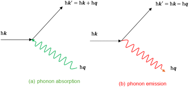
The data in Fig. 1 illustrate the electron scattering by phonon (a) absorption and (b) emission processes in a two-dimensional system.
 |
| | Fig. 1 Illustration of possible electron scattering processes in a two-dimensional system by (a) phonon absorption and (b) phonon emission. Where k is the electron wave vector and q is the phonon wave vector. | |
In this section, the matrix element of acoustic phonon interaction by the 2D electron in III-nitride Pöschl–Teller QW semiconductors, including AlN, GaN, and InN, takes the form23,24,27–33
| |  | (5) |
where
Θ is denoted as the system volume of III-nitride Pöschl–Teller QW semiconductors,
q the wave vector,
ϑ the sound velocity in AlN, GaN, and InN,
ρ the III-nitride mass density, and
ϕ the deformation potential constant. The factor |
Jni,nf(
θ)|
2 has the following form:
| |  | (6) |
Here
θ =
RC2q⊥2/2, and
LN2N1−N2(
θ) is the symbol of the Laguerre polynomials, with the values of
N1 and
N2 determined by using the formulae
N1 = max(
ni,
nf) and
N2 = min(
ni,
nf). Finally, the factor

is denoted as the overlap integral and has the following form
| |  | (7) |
It is well known that in nanostructure semiconductors, particularly at low temperatures, the scattering of carriers by acoustic phonons becomes more significant and can even surpass the scattering of carriers by optical phonons. In this work, we focus on the study of the magneto-optical transport properties of III-nitride QW semiconductors (AlN, GaN, and InN) due to acoustic phonon scattering at low temperatures.
4 Conductivity tensor and absorption power of the magneto-optical transition in III-nitride Pöschl–Teller QW semiconductors resulting from acoustic phonon scattering
4.1 Conductivity tensor of the magneto-optical transition in III-nitride Pöschl–Teller QW semiconductors resulting from acoustic phonon scattering
We present the MO conductivity tensor in III-nitride Pöschl–Teller QW semiconductors, including AlN, GaN, and InN, resulting from acoustic phonon scattering in this subsection. As we know, electronic states undergo quantization in III-nitride Pöschl–Teller QW semiconductors when a B (static magnetic field) is present along the z-axis. At the same time, if AlN, GaN, and InN QW semiconductors are exposed to an electromagnetic wave, then for one, the electrons in these III-nitride Pöschl–Teller QW semiconductors will cause MO transport in which the most prevalent one is the cyclotron one through absorbing an appropriate photon energy. At that time, the MO conductivity tensor in III-nitride Pöschl–Teller QW semiconductors, resulting from acoustic phonon scattering had the following form:34–37| |  | (8) |
with  , κ+ = κx + iκy in which κ+ is denoted by the operators of current density, L by Liouville, and cγ/(cγ+) by Pöschl–Teller QW electron annihilation (creation). In this work, the analytical method is employed, which is the operator projection (OP) method. The definition of this method, which is employed to further transform the MO conductivity tensor formula (8) in III-nitride Pöschl–Teller QW semiconductors, including AlN, GaN, and InN, resulting from acoustic phonon scattering, is as follows:
| |  | (9) |
with the arbitrary operator, Λ, denoted by the following formula 〈Λ〉γ = TR{ρ0[Λ,cγ+cγ+1]}. After completing systematic analytical transformations, we get the MOCT formula in III-nitride Pöschl–Teller QW semiconductors, including AlN, GaN, and InN, resulting from acoustic phonon scattering as| |  | (10) |
In order to derive the ultimate formula for the MO conductivity tensor in III-nitride Pöschl–Teller QW semiconductors, including AlN, GaN, and InN, resulting from acoustic phonon scattering, we employ the AB identity (A − B)−1 = A−1 + A−1B(A − B)−1 and the OP method in formula (9) intended for further transformation of the factor, (ℏ![[small omega, Greek, macron]](https://www.rsc.org/images/entities/i_char_e0da.gif) − L)−1κ+, in formula (10). After completing systematic analytical transformations, we get the MOCT formula resulting from acoustic phonon scattering in III-nitride Pöschl–Teller QW semiconductors (AlN, GaN, and InN) as follows:
− L)−1κ+, in formula (10). After completing systematic analytical transformations, we get the MOCT formula resulting from acoustic phonon scattering in III-nitride Pöschl–Teller QW semiconductors (AlN, GaN, and InN) as follows:
| |  | (11) |
with the Fermi distributions denoted by

and

and the line-width function by

. After completing systematic analytical transformations, we obtain the quantity

in formula
(11) for III-nitride Pöschl–Teller QW semiconductors, including AlN, GaN, and InN, resulting from acoustic phonon scattering, which takes the form
| | 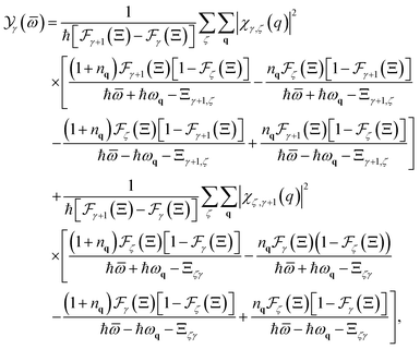 | (12) |
where
nq = 1/[exp(ℏ
ωq/
kBT) − 1] is denoted as the Planck distribution function for acoustic phonons in III-nitride Pöschl–Teller QW semiconductors, including AlN, GaN, and InN.
4.2 Absorption power of the magneto-optical transition in III-nitride Pöschl–Teller QW semiconductors resulting from acoustic phonon scattering
The electronic states undergo quantization in III-nitride Pöschl–Teller QW semiconductors when a B is present along the z-axis. When AlN, GaN, and InN QW semiconductors are exposed to an electromagnetic wave having F0 amplitude, the electron in III-nitride Pöschl–Teller QW semiconductors causes MO transport. At that time, the absorbing power of the MO transition in III-nitride Pöschl–Teller QW semiconductors, resulting from acoustic phonon scattering takes the form:37| | | P(ω) = F02Re{Γ+−(ω)}/2, | (13) |
where the factor Re{ϒ+−(ω)} is denoted as the real part of the CT of the MO transition in III-nitride Pöschl–Teller QW semiconductors, including AlN, GaN, and InN, resulting from acoustic phonon scattering. By performing calculations that are detailed and thorough to obtain Re{ϒ+−(ω)}, the same as shown in the author N. D. Hien's earlier studies,25 the final formula of the absorbing power of the MO transition in III-nitride Pöschl–Teller QW semiconductors resulting from acoustic phonon scattering is written as| |  | (14) |
where  for III-nitride Pöschl–Teller QW semiconductors resulting from acoustic phonon scattering is given by
| | 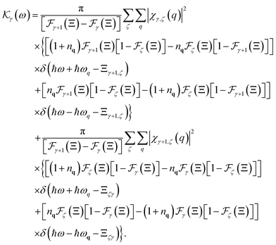 | (15) |
For acoustic phonon scattering in III-nitride Pöschl–Teller QW semiconductors, including AlN, GaN, and InN, we apply the approximation as shown in ref. 38 and 39 that Nq ≈ (Nq + 1) ≈ kBT/(ℏωq). Here, kB is the Boltzmann constant, and ℏωq = ℏϑq. Simultaneously, utilizing the relationships
| |  | (16) |
| |  | (17) |
and carrying out the following systematic and methodical computations of the |
χγ,ζ(
q)|
2 and |
χγ+1,ζ(
q)|
2 matrix elements for

of acoustic phonon scattering by the 2D electron in III-nitride Pöschl–Teller QW semiconductors, including AlN, GaN, and InN, we then obtain the final formula of

as follows:
| | 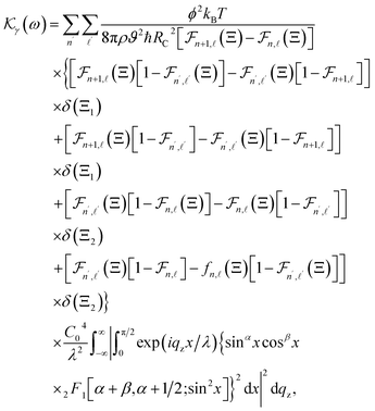 | (18) |
where 0 ≤
x ≤ π/2, and the expressions of
Ξ1 and
Ξ2, take the form
| |  | (19) |
and
| |  | (20) |
Moreover, in eqn (18), the Lorentzian widths40 are denoted by  and
and  used instead of the use of the δ(Ξ1) and δ(Ξ2) Dirac delta functions as the following:
| |  | (21) |
| |  | (22) |
After completing systematic computations of the formula for the  Lorentzian width due to acoustic phonon scattering by the 2D electron in III-nitride Pöschl–Teller QW semiconductors, including AlN, GaN, and InN, we obtain
| |  | (23) |
Note that the integral over dqz, in eqn (18) and (23), resulting from acoustic phonon scattering in III-nitride Pöschl–Teller QW semiconductors, including AlN, GaN, and InN, will be thoroughly numerically evaluated. To achieve the outcomes of the computer calculations and graphic representations by applying the appropriate computational methodologies to the above analytical computation results, reliable outcomes for the MOT properties of III-nitride Pöschl–Teller QW semiconductors, including AlN, GaN, and InN, resulting from acoustic phonon scattering will be drawn in the following section.
5 Numerical results and discussion
The numerical calculations in this section are realized to include (i) the absorption power in III-nitride Pöschl–Teller QW semiconductors, including InN, AlN, and GaN resulting from the acoustic phonon scattering at the various QS temperatures, QW thicknesses, and magnetic fields versus the photon energy. (ii) The absorbing FWHM dependencies in III-nitride Pöschl–Teller QW semiconductors, including InN, AlN, and GaN resulting from the acoustic phonon scattering at the various QS temperatures, QW thicknesses, and magnetic fields. (iii) Comparison of the absorbing power in III-nitride Pöschl–Teller and square QW semiconductors, including InN, AlN, and GaN, resulting from the acoustic phonon scattering. (iv) Comparison of the absorbing FWHM dependencies in III-nitride Pöschl–Teller and square QW semiconductors, including InN, AlN, and GaN, resulting from the acoustic phonon scattering at the QS temperature, QW thickness, and applied magnetic field. The specific results are displayed in the figures below:
Fig. 2 displays the data as the result of the profiles and wave functions of the Pöschl–Teller confined potential at β = 2.6 and LW = 12.65 nm for seven values of α including α = 1.4, 1.8, 2.2, 2.6, 3.0, 3.4, and 3.8. This result indicates that the Pöschl–Teller confined potential profile is fully symmetric at α = β = 2.6, and on the other hand, asymmetric at α ≠ β. This is similar to the data in ref. 41. Simultaneously, the data also illustrate that the profile is moved above when α > 2.6, and below when α < 2.6. Our findings are regarded as reasonable (Table 1).
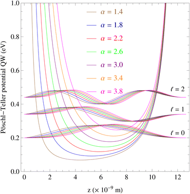 |
| | Fig. 2 The profiles and wave functions of the Pöschl–Teller confined potential at β = 2.6, LW = 12.65 nm, and α = 1.4, 1.8, 2.2, 2.6, 3.0, 3.4, and 3.8. | |
Table 1 III-Nitride semiconductor parameters, including InN, AlN, and GaN, used in calculations:12,42
| Parameters |
GaN |
AlN |
InN |

|
0.22 |
0.29 |
0.045 |
|
ρ (g cm−3) |
6.09 |
3.23 |
6.81 |
|
ϕ (eV) |
8.3 |
9.5 |
7.1 |
|
ϑ (×105 cm s−1) |
4.40 |
6.04 |
4.15 |
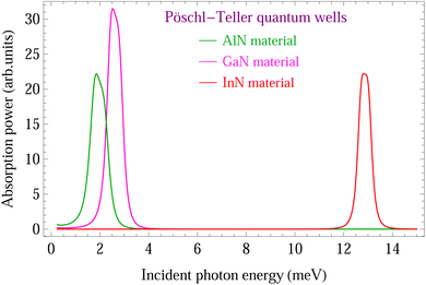
Fig. 3 shows numerical result of the absorption power in III-nitride Pöschl–Teller QW semiconductors, including InN, AlN, and GaN, resulting from the acoustic phonon scattering at a QW thickness of 5 nm, an applied magnetic field of 5T, and a QS temperature of 37 K, versus the photon energy, where asymmetry-degree-adjusted parameters α = 3 and β = 2. The colour curves, respectively, represent the InN, AlN, and GaN materials in green, magenta, and red. We are able to see evidently from the absorption spectrum that each III-nitride Pöschl–Teller QW semiconductor, including InN, AlN, and GaN, corresponds to one evident resonance peak. By utilising computational techniques and the resonant phenomenon condition, we determine that when a magnetic field is present, the two-dimensional confining electrons in InN, AlN, and GaN absorb the corresponding 2.00 meV, 2.63 meV, and 12.87 meV photon energies (ℏω) to create the cyclotron resonance (CR) transitions. Namely, the position of CR transition absorbing peaks in III-nitride Pöschl–Teller QW semiconductors, including InN, AlN, and GaN, resulting from the acoustic phonon scattering satisfies resonant condition (n′ − n)ℏωc = ℏω ≡ 2.00 meV, (n′ − n)ℏωc = ℏω ≡ 2.63 meV, and (n′ – n)ℏωc = ℏω ≡ 12.87 meV, respectively. In this calculation, transitions between the n = 0 and n′ = 1, the lowest Landau levels are taken into account. The CR absorbing transition of the electron in III-nitride Pöschl–Teller QW semiconductors, including InN, AlN, and GaN, resulting from acoustic phonon scattering is described such that the two-dimensional confining electrons in InN, AlN, and GaN absorb the corresponding 2.00 meV, 2.63 meV, and 12.87 meV photon energies, resulting from the acoustic phonon scattering in order to create the cyclotron resonance (CR) transitions from the n = 0 Landau level to the n′ = 1 Landau level.
 |
| | Fig. 3 Absorption power in III-nitride Pöschl–Teller QW semiconductors, including InN, AlN, and GaN, resulting from the acoustic phonon scattering at a QW thickness of 5 nm, an applied magnetic field of 5T, and a QS temperature of 37 K, versus the photon energy, where asymmetry-degree-adjusted parameters α = 3 and β = 2. The colour curves, respectively, represent the InN, AlN, and GaN materials in green, magenta, and red. | |
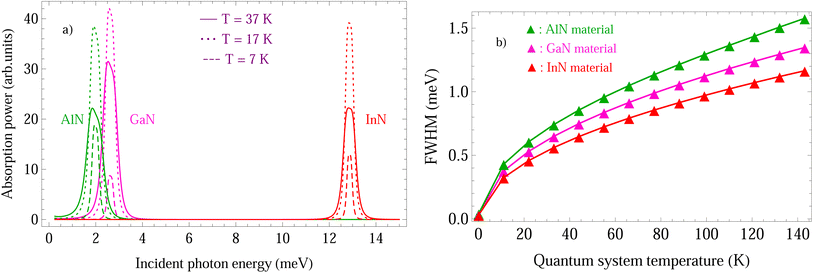
In Fig. 4, the absorbing power in III-nitride Pöschl–Teller QW semiconductors, including InN, AlN, and GaN, resulting from the acoustic phonon scattering at the various QS temperatures for a QW thickness of 5 nm and an applied magnetic field of 5T, versus the photon energy, is displayed. Note that in this numerical calculation, asymmetry-degree-adjusted parameters α = 3 and β = 2. The colour curves, respectively, represent the InN, AlN, and GaN materials in green, magenta, and red. The solid, dotted, and dashed curves, respectively, represent the QS temperatures of 37 K, 17 K, and 7 K. The results in the figure evidently demonstrate that the QS temperature has an evident impact on the absorbing spectrum intensity. Contrary to this, the influence of these low temperatures on the resonant peak's position is insignificant and can be neglected. The distribution function,  , of the electron in III-nitride Pöschl–Teller QW semiconductors, including AlN, GaN, and InN, is dependent on the QS temperature, which provides an explanation for this feature of the absorbing spectrum intensity, resulting from the acoustic phonon scattering. Namely, we are able to see evidently from expression
  that it is proportional to e−1/T, wherefore, it has an evident change as the QS temperature varies. This leads to the absorbing spectrum intensity in III-nitride Pöschl–Teller QW semiconductors, including InN, AlN, and GaN, resulting from the acoustic phonon scattering being affected appreciably by the QS temperature. On the other hand, the QS temperature completely has no impact on the absorbing spectrum position in III-nitride Pöschl–Teller QW semiconductors, including InN, AlN, and GaN, resulting from acoustic phonon scattering. This is easily understood by observation of the following formulae (18)–(20), in which the QS temperature is absent from the factors Ξ1 and Ξ2 regarding the Dirac delta functions, namely δ(Ξ1) and δ(Ξ2). In addition, another way to interpret this physical characteristic is that the absorbing spectrum position in III-nitride Pöschl–Teller QW semiconductors, including InN, AlN, and GaN, resulting from acoustic phonon scattering, meets the requirement for the CR phenomenon, nℏωc + ℏω = n′ℏωc, where we are able to see evidently from this expression that it is evidently unaffected by the QS temperature. The results obtained in (Fig. 4b) are the absorbing FWHM dependency in III-nitride Pöschl–Teller QW semiconductors, including InN, AlN, and GaN, resulting from the acoustic phonon scattering on the QS temperature at the same parameter values as above. We are able to see evidently from the figure that at low temperatures of quantum systems (T < 150 K), the higher the QS temperature values are, the greater the absorbing FWHM values will be, i.e., if the QS temperatures in III-nitride Pöschl–Teller QW semiconductors, including InN, AlN, and GaN, increase, then their absorbing FWHMs resulting from the acoustic phonon scattering increase. This characteristic of III-nitride semiconductors can be interpreted based on the fact that the acoustic phonon scattering probabilities in III-nitride Pöschl–Teller QW semiconductors, including InN, AlN, and GaN are augmented evidently as the enhanced QS temperatures. Our theoretical study outcomes will provide further qualitative evidence to confirm the early experimental ones in ref. 15 and 43–45. In particular, our findings demonstrate that the absorbing FWHM dependency on the QS temperature in the GaN Pöschl–Teller QW semiconductor is weaker than that in the AlN one, while stronger in the InN one. Among InN, AlN, and GaN materials, the absorbing FWHMs in AlN are the greatest and the fastest increasing; inversely, they are the smallest and the slowest increasing in InN. Our findings offer valuable information for the advancement of electronic devices.
 |
| | Fig. 4 (a) Absorption power in III-nitride Pöschl–Teller QW semiconductors, including AlN, GaN, and InN, resulting from the acoustic phonon scattering at the various QS temperatures for a QW thickness of 5 nm and an applied magnetic field of 5T, versus the photon energy, where asymmetry-degree-adjusted parameters α = 3 and β = 2. The colour curves, respectively, represent the AlN, GaN, and InN materials in green, magenta, and red. The solid, dotted, and dashed curves, respectively, represent the QS temperatures of 37 K, 17 K, and 7 K. (b) The absorbing FWHM dependency in III-nitride Pöschl–Teller QW semiconductors, including AlN, GaN, and InN, resulting from the acoustic phonon scattering on the QS temperature at the same parameter values as above. | |
Besides the impact of QS temperature on the MOTPs of III-nitride Pöschl–Teller QW semiconductors, including AlN, InN, and GaN, resulting from the acoustic phonon scattering as analysed above, the impact of QW thickness on their MOTPs was also thoroughly taken into account, and the outcomes obtained are as follows: firstly, the absorbing power in III-nitride Pöschl–Teller QW semiconductors, including AlN, InN, and GaN, resulting from the acoustic phonon scattering at the various QW thicknesses for an applied magnetic field of 5 T and a QS temperature of 37 K, versus the photon energy is demonstrated in in Fig. 5a, where asymmetry-degree-adjusted parameters α = 3 and β = 2. The colour curves, respectively, represent the AlN, GaN, and InN materials in green, magenta, and red. The solid, dotted, and dashed curves, respectively, represent the QW widths of 5 nm, 7 nm, and 9 nm. As can be seen from the figure the QW thickness has an evident impact on the absorbing spectrum intensity. Contrary to this, it completely has no impact on the absorbing spectrum position in III-nitride Pöschl–Teller QW semiconductors, including AlN, InN, and GaN, resulting from acoustic phonon scattering. This feature bears resemblance to the QS temperature case; however, the interpretation for this characteristic is not completely similar to that for the QS temperature case. Namely, the QW thickness completely has no impact on the absorbing spectrum position in III-nitride Pöschl–Teller QW semiconductors, including AlN, InN, and GaN, resulting from acoustic phonon scattering. This is easily understood by the observation of the following formulae of the CR condition, nℏωc + ℏω = n′ℏωc, where we are able to see evidently from this expression that it is evidently unaffected by the QW thickness. Furthermore, this characteristic is also easily understood by observation of the following formulae of the electronic energies (19) and (20) and of the line-width function in (18) for the Pöschl–Teller QW is that the Ξ1 and Ξ2 quantities related to δ(Ξ1) and δ(Ξ2) delta functions of the Dirac are evident dependent on the QW thickness. This leads to the absorbing spectrum intensity in III-nitride Pöschl–Teller QW semiconductors, including AlN, GaN, and InN, resulting from the acoustic phonon scattering being affected evidently by the QW thickness. Secondly, an additional important feature illustrated evidently in Fig. 5b is the absorbing FWHM dependency in III-nitride Pöschl–Teller QW semiconductors, including AlN, InN, and GaN, resulting from the acoustic phonon scattering on the QW thickness. Based on the figure, it is clear that the greater the QW thickness values are, the smaller the absorbing FWHM values will be, i.e., if the thickness of III-nitride Pöschl–Teller QW semiconductors, including AlN, InN, and GaN, increase, then their absorbing FWHMs resulting from the acoustic phonon scattering diminish. Our theoretical study outcomes will provide further qualitative evidence to confirm the early experimental ones in ref. 15, 44 and 46. The acoustic phonon scattering probabilities in III-nitride Pöschl–Teller QW semiconductors, such as AlN, InN, and GaN, are diminished evidently with augmented QW thickness, which explains this property of III-nitride semiconductors. Further understanding of this characteristic also suggests that an evident increment in the QW thickness (LW) results in an appreciable decrement of the lowest sub-band levels' energy separation,  . The result is that acoustic phonon scattering probabilities in III-nitride Pöschl–Teller QW semiconductors (AlN, GaN, and InN) are quickly reduced, and hence the absorbing spectrum FWHMs, regarding acoustic phonon scattering appreciably decrease. More specifically, our outcomes demonstrate that the absorbing FWHM dependency on the QW thickness in the GaN Pöschl–Teller QW semiconductor is weaker in the AlN one, while stronger in the InN one. Among AlN, InN, and GaN materials, the absorbing FWHMs in AlN are the greatest and the fastest diminishing; inversely, they are the smallest and the slowest diminishing in InN. This characteristic of III-nitride Pöschl–Teller QW semiconductors is more evident when the QW thickness is sufficiently low. To be more precise, this characteristic suggests that in two-dimensional III-nitride materials, including AlN, InN, and GaN, acoustic phonon scattering is more meaningful than that in bulk III-nitride materials.
 |
| | Fig. 5 (a) Absorption power in III-nitride Pöschl–Teller QW semiconductors, including AlN, InN, and GaN, resulting from the acoustic phonon scattering at the various QW thicknesses for an applied magnetic field of 5T and a QS temperature of 37 K, versus the photon energy, where asymmetry-degree-adjusted parameters α = 3 and β = 2. The colour curves, respectively, represent the AlN, GaN, and InN materials in green, magenta, and red. The solid, dotted, and dashed curves, respectively, represent the QW widths of 5 nm, 7 nm, and 9 nm. (b) The absorbing FWHM dependency in III-nitride Pöschl–Teller QW semiconductors, including AlN, InN, and GaN, resulting from the acoustic phonon scattering on the QW thickness at the same parameter values as above. | |
In this research, the external field impact on the MOTPs of III-nitride Pöschl–Teller QW semiconductors, including AlN, InN, and GaN, resulting from acoustic phonon scattering, is also thoroughly investigated. The following are the outcomes obtained: first, the absorbing power in III-nitride Pöschl–Teller QW semiconductors, including AlN, GaN, and InN, resulting from the acoustic phonon scattering at the various applied magnetic fields for a QW thickness of 5 nm and a QS temperature of 37 K, versus the photon energy is demonstrated in Fig. 6a, where asymmetry-degree-adjusted parameters α = 3 and β = 2. The colour curves, respectively, represent the AlN, GaN, and InN materials in green, magenta, and red. The solid, dotted, and dashed curves, respectively, represent the various applied magnetic fields of 5 Tesla, 6 Tesla, and 7 Tesla. After analysing the data in Fig. 6a, we can also draw the following conclusions: different from the QW thickness and the QS temperature, the applied magnetic field not only has an evident impact on the absorption spectrum intensity but also has an appreciable impact on the absorption spectrum position in III-nitride Pöschl–Teller QW semiconductors, including AlN, GaN, and InN, resulting from acoustic phonon scattering. Specifically as follows, if there is an enhancement of the applied magnetic field, then the absorption spectrum position in III-nitride Pöschl–Teller QW semiconductors, including AlN, GaN, and InN, resulting from acoustic phonon scattering, is blue-shifted. Observing the following formulae makes it easy to understand that this cause is a result of the CR condition. We can see clearly from this expression that it is affected by the applied magnetic field (B): nℏωc + ℏω = n′ℏωc in which  . We consider n = 0 and n′ = 1 in this calculation, wherefore the formula of the photon energy is
  . This results in ℏω being enhanced as B increases. So, if there is an enhancement of the applied magnetic field, then the absorption spectrum position in III-nitride Pöschl–Teller QW semiconductors, including AlN, GaN, and InN, resulting from acoustic phonon scattering, is blue-shifted. More importantly, analysis of the data in Fig. 6a leads us to the conclusion that among III-nitride Pöschl–Teller QW semiconductors, including AlN, GaN, and InN, the impact of the external field on the absorption spectrum position of the InN semiconductor, resulting from acoustic phonon scattering is the strongest. This finding could provide useful data for optoelectronic device manufacturing. Moreover, the external field has an appreciable impact on the absorption spectrum's intensity in III-nitride Pöschl–Teller QW semiconductors, including AlN, GaN, and InN, resulting from acoustic phonon scattering, i.e., it has an appreciable change when varying the value of B. The cause of this occurrence is because the acoustic phonon scattering probability in III-nitride Pöschl–Teller QW semiconductors, including AlN, GaN, and InN appreciably changes when varying the value of B. The cyclotron radius expression
  can help us to be able to understand and clarify this. Another important feature also illustrated evidently in Fig. 6b is the absorbing FWHM dependency in III-nitride Pöschl–Teller QW semiconductors, including AlN, GaN, and InN, resulting from the acoustic phonon scattering on the magnetic field. We can also draw the following conclusions after analysing the data in Fig. 6b: (i) the absorbing FWHM in III-nitride Pöschl–Teller QW semiconductors, including AlN, GaN, and InN, resulting from the acoustic phonon scattering is a function of B; (ii) the greater the magnetic field values are, the greater the absorbing FWHM values will be, i.e., if the applied magnetic field in III-nitride Pöschl–Teller QW semiconductors, including AlN, GaN, and InN, increase, then their absorbing FWHMs resulting from the acoustic phonon scattering, increase. The cause of this occurrence is because, the greater the B applied magnetic field in III-nitride Pöschl–Teller QW semiconductors, the smaller the two dimensional electron cyclotron radius
  , the stronger the confinement intensity of a two dimensional electron, the bigger the acoustic phonon scattering probability, and the greater the absorbing spectrum FWHM in III-nitride Pöschl–Teller QW semiconductors, including AlN, GaN, and InN will be. Our theoretical study outcomes will provide further qualitative evidence to confirm the early experimental ones in ref. 47 and 48. In addition, after analysing the data in Fig. 6 b, we can also draw the following conclusions: the absorbing FWHM dependency on the applied magnetic field in the GaN Pöschl–Teller QW semiconductor is stronger in the InN one, and weaker in the AlN one. Among III-nitride materials, including AlN, GaN, and InN, the absorbing FWHMs in AlN are the greatest and the fastest diminishing; inversely, they are the smallest and the slowest diminishing in InN. These features are similar to those in the cases of the QW thickness and QS temperature. However, the characteristic of the magnetic field impact on the absorption spectrum position in III-nitride Pöschl–Teller QW semiconductors, including AlN, GaN, and InN, resulting from acoustic phonon scattering is very different from the cases of the QS temperature and the QW thickness, which have been mentioned above.
 |
| | Fig. 6 (a) Absorption power in III-nitride Pöschl–Teller QW semiconductors, including AlN, InN, and GaN, resulting from the acoustic phonon scattering at the various applied magnetic fields for a QW thickness of 5 nm and a QS temperature of 37 K, versus the photon energy, where asymmetry-degree-adjusted parameters α = 3 and β = 2. The colour curves, respectively, represent the AlN, GaN, and InN materials in green, magenta, and red. The solid, dotted, and dashed curves, respectively, represent the various applied magnetic fields of 5 Tesla, 6 Tesla, and 7 Tesla. (b) The absorbing FWHM dependency in III-nitride Pöschl–Teller QW semiconductors, including AlN, InN, and GaN, resulting from the acoustic phonon scattering on the applied magnetic field at the same parameter values as above. | |
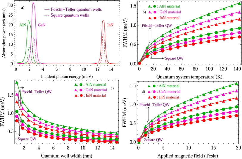
Especially in this research, the results obtained for III-nitride Pöschl–Teller QW semiconductors are thoroughly compared with those for III-nitride square QW ones. First, the data in Fig. 7a are the result of the comparison of the absorbing power in III-nitride Pöschl–Teller and square QW semiconductors, including AlN, InN, and GaN, resulting from the acoustic phonon scattering at a QW thickness of 5 nm, an applied magnetic field of 5 T, and a QS temperature of 37 K, versus the photon energy, where asymmetry-degree-adjusted parameters α = 3 and β = 2. The colour curves, respectively, represent the AlN, GaN, and InN materials in green, magenta, and red. The solid and dashed curves, respectively, represent the Pöschl–Teller and square QWs. As seen in Fig. 7a, there is an evident difference in the absorption spectrum intensity between the Pöschl–Teller and square QWs of III-nitride semiconductors, including AlN, InN, and GaN, resulting from acoustic phonon scattering. Secondly, the data in Fig. 7b–d are the results of the comparisons of the absorbing FWHM dependencies in III-nitride Pöschl–Teller and square semiconductors, including AlN, InN, and GaN, resulting from the acoustic phonon scattering on the QS temperature, the QW thickness, and the applied magnetic field, respectively. The results demonstrate that the absorbing FWHMs resulting from the acoustic phonon scattering in III-nitride materials (AlN, InN, and GaN) increase with an increasing QS temperature and applied magnetic field; conversely, they diminish with an increasing QW thickness for both the Pöschl–Teller and square semiconductors. Specifically, the results also prove that the absorbing FWHMs of III-nitride materials (AlN, GaN, and InN) resulting from the acoustic phonon scattering in Pöschl–Teller QW semiconductors always have greater values and faster variation in comparison with square QW semiconductors. Therefore, the absorbing FWHMs of III-nitride semiconductors resulting from acoustic phonon scattering are strongly dependent on the nanostructure's geometric shape.
 |
| | Fig. 7 (a) Comparison of the absorbing power in III-nitride Pöschl–Teller and square QW semiconductors, including AlN, GaN, and InN, resulting from the acoustic phonon scattering at a QW thickness of 5 nm, an applied magnetic field of 5 T, and a QS temperature of 37 K, versus the photon energy, where asymmetry-degree-adjusted parameters α = 3 and β = 2. The colour curves, respectively, represent the AlN, GaN, and InN materials in green, magenta, and red. The solid and dashed curves, respectively, represent the Pöschl–Teller and square QWs. (b) Comparison of the absorbing FWHM dependency in III-nitride Pöschl–Teller and square semiconductors, including AlN, GaN, and InN, resulting from the acoustic phonon scattering on the QS temperature at the same parameter values as above. (c) Comparison of the absorbing FWHM dependency in III-nitride Pöschl–Teller and square semiconductors, including AlN, GaN, and InN, resulting from the acoustic phonon scattering on the QW thickness at the same parameter values as above. (d) Comparison of the absorbing FWHM dependency in III-nitride Pöschl–Teller and square semiconductors, including AlN, GaN, and InN, resulting from the acoustic phonon scattering on the applied magnetic field at the same parameter values as above. | |
In summary, the temperature, thickness, and confinement potential shape strongly influence the intensity and FWHM of the resonance peak while they insignificantly influence its position. In particular, the external magnetic field strongly influences the position, intensity, and FWHM of the resonance peak. These influences are immediately apparent in a comprehensive summary (Table 2) below.
Table 2 The summary of the influences of the temperature, thickness, external magnetic field, and confinement potential shape on the characteristics of the resonance peak
| Influencing factor |
Characteristics of the resonance peak |
| Position of the peak |
Intensity of the peak |
FWHM of the peak |
| Temperature |
Insignificant influence |
Strong influence |
Strong influence |
| Thickness |
Insignificant influence |
Strong influence |
Strong influence |
| Magnetic field |
Strong influence |
Strong influence |
Strong influence |
| Potential shape |
Insignificant influence |
Strong influence |
Strong influence |
6 Conclusions
In summary, applying the technique of operator projection, the MOT properties of III-nitride Pöschl–Teller QW semiconductors, including AlN, GaN, and InN, resulting from the acoustic phonons scattering are thoroughly investigated and compared. In particular, a comparison is made between the Pöschl–Teller QW results and the square QW ones. The following are our research results: (i) for acoustic phonon scattering, the QS temperature, applied magnetic field, and QW width strongly affect the MOT properties of III-nitride Pöschl–Teller QW semiconductors, including AlN, GaN, and InN. (ii) When the applied magnetic field and QS temperature increase, the absorbing FWHM in AlN, GaN, and InN increases; on the other hand, it diminishes when the QW width increases. (iii) The absorbing FWHM dependency on the applied magnetic field and QS temperature, and QW width in GaN Pöschl–Teller QW semiconductor is weaker in the AlN one, and stronger in the InN one. (iv) Among AlN, GaN, and InN materials, the absorbing FWHMs in AlN are the greatest and vary the fastest; inversely, they are the smallest and vary the slowest in InN. The MOTPs of III-nitride Pöschl–Teller QW semiconductors, including AlN, InN, and GaN resulting from acoustic phonon scattering, are more dominant than those of the square QW ones. Our findings offer valuable information for the advancement of electronic devices.
Data availability
Data available on request from the authors.
Author contributions
Ho Kim Dan: investigation, conceptualization, software, writing – original draft, funding acquisition, writing – review and editing. Pham Tuan Vinh: methodology, software, writing – review and editing. Nguyen Dinh Hien: software, methodology, conceptualization, investigation, supervision, writing – review and editing, validation, writing – original draft, funding acquisition.
Conflicts of interest
There are no conflicts to declare.
References
- C. X. Ren, Mater. Sci. Technol., 2016, 32, 418–433 CrossRef CAS.
-
G. Lükens, Normally-off transistor topologies in gallium nitride technology, PhD Thesis, Rheinisch-Westfälische Technische Hochschule Aachen, 2020.
- R. Oliver, Mater. Sci. Technol., 2002, 18, 1257–1271 CrossRef CAS.
- I. A. I. Akasaki and H. A. H. Amano, Jpn. J. Appl. Phys., 1997, 36, 5393 CrossRef CAS.
- M. Asif Khan, J. N. Kuznia, D. T. Olson, W. J. Schaff, J. W. Burm and M. S. Shur, Appl. Phys. Lett., 1994, 65, 1121–1123 CrossRef.
- D. K. Ferry, Phys. Rev. B: Solid State, 1975, 12, 2361–2369 CrossRef CAS.
- C. G. Rodrigues and R. Luzzi, Pramana – J. Phys., 2021, 95, 7053 CrossRef.
- X. B. Zhang, T. Taliercio, S. Kolliakos and P. Lefebvre, J. Phys.: Condens. Matter, 2001, 13, 7053 CrossRef CAS.
- J.-J. Shi, X.-L. Chu and E. M. Goldys, Phys. Rev. B: Condens. Matter Mater. Phys., 2004, 70, 115318 CrossRef.
- I. Boyko, M. Petryk and J. Fraissard, Superlattices Microstruct., 2021, 156, 106928 CrossRef CAS.
- W. D. Huang, Y. J. Ren, S. Y. Wei and J. H. Wang, Eur. Phys. J. Appl. Phys., 2008, 43, 73–77 CrossRef CAS.
- Z. W. Yan, S. L. Ban and X. X. Liang, Eur. Phys. J. B, 2003, 35, 41 CrossRef CAS.
- J. S. Bhat, R. A. Nesargi and B. G. Mulimani, J. Appl. Phys., 2009, 106, 033701 CrossRef.
- J. Y. Sug, S. G. Jo, J. Kim, J. H. Lee and S. D. Choi, Phys. Rev. B: Condens. Matter Mater. Phys., 2001, 64, 235210 CrossRef.
- T. Unuma, M. Yoshita, T. Noda, H. Sakaki and H. Akiyama, J. Appl. Phys., 2003, 93, 1586–1597 CrossRef CAS.
- J. Faist, F. Capasso, D. L. Sivco, C. Sirtori, A. L. Hutchinson and A. Y. Cho, Science, 1994, 264, 553–556 CrossRef CAS.
- B. F. Levine, J. Appl. Phys., 1993, 74, R1–R81 CrossRef CAS.
- H. Yıldır ım and M. Tomak, Phys. Rev. B: Condens. Matter Mater. Phys., 2005, 72, 115340 CrossRef.
- S. Şakiroğlu, F. Ungan, U. Yesilgul, M. E. Mora-Ramos, C. A. Duque, E. Kasapoglu, H. Sari and İ. Sökmen, Phys. Lett. A, 2012, 376, 1875–1880 CrossRef.
- K. D. Pham, L. V. Tung, D. V. Thuan, C. V. Nguyen, N. N. Hieu and H. V. Phuc, J. Appl. Phys., 2019, 126, 124301 CrossRef.
- H. Yildirim and M. Tomak, J. Appl. Phys., 2006, 99, 093103 CrossRef.
- N. D. Hien, Phys. E Low-dimens. Syst. Nanostruct., 2023, 145, 115504 CrossRef CAS.
- N. D. Hien, Micro Nanostruct., 2022, 167, 207236 CrossRef CAS.
- N. D. Hien, J. Phys. Chem. Solids, 2022, 167, 110757 CrossRef CAS.
- N. D. Hien, J. Phys. Chem. Solids, 2022, 161, 110456 CrossRef CAS.
- N. D. Hien, Phys. B, 2022, 638, 413901 CrossRef CAS.
- J. S. Bhat, S. S. Kubakaddi and B. G. Mulimani, J. Appl. Phys., 1991, 70, 2216–2219 CrossRef CAS.
- Y. J. Cho and S. D. Choi, Phys. Rev. B: Condens. Matter Mater. Phys., 1994, 49, 14301–14306 CrossRef CAS.
- N. Kang, Y. Ji, H. J. Lee and S. Choi, J. Korean Phys. Soc., 2003, 42, 379–385 CAS.
- N. Kang, Y. Lee and S. Choi, J. Korean Phys. Soc., 2004, 44, 1535–1541 CAS.
- P. Vasilopoulos, Phys. Rev. B: Condens. Matter Mater. Phys., 1986, 33, 8587–8594 CrossRef.
- G.-Q. Hai and F. M. Peeters, Phys. Rev. B: Condens. Matter Mater. Phys., 1999, 60, 8984–8991 CrossRef CAS.
- T. C. Phong, L. N. Minh and N. D. Hien, Nanoscale Adv., 2024, 6, 832–845 RSC.
- N. L. Kang, S. D. Choi and Y. J. Cho, Prog. Theor. Phys., 1996, 96, 307–316 CrossRef CAS.
- N. Lyong Kang, J. H. Lee and D.-S. Choi, J. Korean Phys. Soc., 2000, 37, 339–342 Search PubMed.
- J. Yon Ryu, Y. Choon Chung and S. Don Choi, Phys. Rev. B: Condens. Matter Mater. Phys., 1985, 32, 7769–7775 CrossRef CAS.
- J. Y. Sug, S. G. Jo, J. Kim, J. H. Lee and S. D. Choi, Phys. Rev. B: Condens. Matter Mater. Phys., 2001, 64, 235210 CrossRef.
- H. Kobori, T. Ohyama and E. Otsuka, J. Phys. Soc. Jpn., 1990, 59, 2141–2163 CrossRef CAS.
- P. Vasilopoulos, Phys. Rev. B: Condens. Matter Mater. Phys., 1986, 33, 8587–8594 CrossRef.
- M. P. Chaubey and C. M. Van Vliet, Phys. Rev. B: Condens. Matter Mater. Phys., 1986, 33, 5617–5622 CrossRef.
- N. D. Hien, J. Phys. Chem. Solids, 2023, 179, 111373 CrossRef CAS.
- R. Zheng, T. Taguchi and M. Matsuura, Phys. Rev. B: Condens. Matter Mater. Phys., 2002, 66, 075327 CrossRef.
- T. Unuma, T. Takahashi, T. Noda, M. Yoshita, H. Sakaki, M. Baba and H. Akiyama, Appl. Phys. Lett., 2001, 78, 3448–3450 CrossRef CAS.
- K. L. Campman, H. Schmidt, A. Imamoglu and A. C. Gossard, Appl. Phys. Lett., 1996, 69, 2554–2556 CrossRef CAS.
- Y. Gu, Y. G. Zhang, X. Y. Chen, S. P. Xi, B. Du and Y. J. Ma, Appl. Phys. Lett., 2015, 107, 212104 CrossRef.
- M. Belmoubarik, K. Ohtani and H. Ohno, Appl. Phys. Lett., 2008, 92, 191906 CrossRef.
- M. Singh, Phys. Rev. B: Condens. Matter Mater. Phys., 1987, 35, 9301–9304 CrossRef.
- N. Holonyak, R. M. Kolbas, W. D. Laidig, M. Altarelli, R. D. Dupuis and P. D. Dapkus, Appl. Phys. Lett., 1979, 34, 502–505 CrossRef CAS.
|
| This journal is © The Royal Society of Chemistry 2024 |
Click here to see how this site uses Cookies. View our privacy policy here.  Open Access Article
 ab,
Pham Tuan
Vinh
 c and
Nguyen Dinh
Hien
 *de
*de

 and respective eigenvalue
  when along the z-axis present a static magnetic field:23–26
 , respectively, in which x0 = −kyRC2, with RC = (cℏ/(|e|B))1/2. In eqn (2), n = 0, 1, 2, … is denoted as the Landau levels (LLs), and
  the subband levels. Then, z-composition's wave function in III-nitride Pöschl–Teller QW semiconductors takes the form of:20–22
 and
and  are denoted as the hypergeometric function and normalization constant. Finally, the respective eigenvalue,
  , as
, as
 is denoted as the cyclotron frequency.


 is denoted as the overlap integral and has the following form

 , κ+ = κx + iκy in which κ+ is denoted by the operators of current density, L by Liouville, and cγ/(cγ+) by Pöschl–Teller QW electron annihilation (creation). In this work, the analytical method is employed, which is the operator projection (OP) method. The definition of this method, which is employed to further transform the MO conductivity tensor formula (8) in III-nitride Pöschl–Teller QW semiconductors, including AlN, GaN, and InN, resulting from acoustic phonon scattering, is as follows:

![[small omega, Greek, macron]](https://www.rsc.org/images/entities/i_char_e0da.gif) − L)−1κ+, in formula (10). After completing systematic analytical transformations, we get the MOCT formula resulting from acoustic phonon scattering in III-nitride Pöschl–Teller QW semiconductors (AlN, GaN, and InN) as follows:
− L)−1κ+, in formula (10). After completing systematic analytical transformations, we get the MOCT formula resulting from acoustic phonon scattering in III-nitride Pöschl–Teller QW semiconductors (AlN, GaN, and InN) as follows:
 and
and  and the line-width function by
  . After completing systematic analytical transformations, we obtain the quantity
  in formula (11) for III-nitride Pöschl–Teller QW semiconductors, including AlN, GaN, and InN, resulting from acoustic phonon scattering, which takes the form

 for III-nitride Pöschl–Teller QW semiconductors resulting from acoustic phonon scattering is given by


 of acoustic phonon scattering by the 2D electron in III-nitride Pöschl–Teller QW semiconductors, including AlN, GaN, and InN, we then obtain the final formula of
  as follows:


 and
and  used instead of the use of the δ(Ξ1) and δ(Ξ2) Dirac delta functions as the following:

 Lorentzian width due to acoustic phonon scattering by the 2D electron in III-nitride Pöschl–Teller QW semiconductors, including AlN, GaN, and InN, we obtain

 , of the electron in III-nitride Pöschl–Teller QW semiconductors, including AlN, GaN, and InN, is dependent on the QS temperature, which provides an explanation for this feature of the absorbing spectrum intensity, resulting from the acoustic phonon scattering. Namely, we are able to see evidently from expression
  that it is proportional to e−1/T, wherefore, it has an evident change as the QS temperature varies. This leads to the absorbing spectrum intensity in III-nitride Pöschl–Teller QW semiconductors, including InN, AlN, and GaN, resulting from the acoustic phonon scattering being affected appreciably by the QS temperature. On the other hand, the QS temperature completely has no impact on the absorbing spectrum position in III-nitride Pöschl–Teller QW semiconductors, including InN, AlN, and GaN, resulting from acoustic phonon scattering. This is easily understood by observation of the following formulae (18)–(20), in which the QS temperature is absent from the factors Ξ1 and Ξ2 regarding the Dirac delta functions, namely δ(Ξ1) and δ(Ξ2). In addition, another way to interpret this physical characteristic is that the absorbing spectrum position in III-nitride Pöschl–Teller QW semiconductors, including InN, AlN, and GaN, resulting from acoustic phonon scattering, meets the requirement for the CR phenomenon, nℏωc + ℏω = n′ℏωc, where we are able to see evidently from this expression that it is evidently unaffected by the QS temperature. The results obtained in (Fig. 4b) are the absorbing FWHM dependency in III-nitride Pöschl–Teller QW semiconductors, including InN, AlN, and GaN, resulting from the acoustic phonon scattering on the QS temperature at the same parameter values as above. We are able to see evidently from the figure that at low temperatures of quantum systems (T < 150 K), the higher the QS temperature values are, the greater the absorbing FWHM values will be, i.e., if the QS temperatures in III-nitride Pöschl–Teller QW semiconductors, including InN, AlN, and GaN, increase, then their absorbing FWHMs resulting from the acoustic phonon scattering increase. This characteristic of III-nitride semiconductors can be interpreted based on the fact that the acoustic phonon scattering probabilities in III-nitride Pöschl–Teller QW semiconductors, including InN, AlN, and GaN are augmented evidently as the enhanced QS temperatures. Our theoretical study outcomes will provide further qualitative evidence to confirm the early experimental ones in ref. 15 and 43–45. In particular, our findings demonstrate that the absorbing FWHM dependency on the QS temperature in the GaN Pöschl–Teller QW semiconductor is weaker than that in the AlN one, while stronger in the InN one. Among InN, AlN, and GaN materials, the absorbing FWHMs in AlN are the greatest and the fastest increasing; inversely, they are the smallest and the slowest increasing in InN. Our findings offer valuable information for the advancement of electronic devices.
 . The result is that acoustic phonon scattering probabilities in III-nitride Pöschl–Teller QW semiconductors (AlN, GaN, and InN) are quickly reduced, and hence the absorbing spectrum FWHMs, regarding acoustic phonon scattering appreciably decrease. More specifically, our outcomes demonstrate that the absorbing FWHM dependency on the QW thickness in the GaN Pöschl–Teller QW semiconductor is weaker in the AlN one, while stronger in the InN one. Among AlN, InN, and GaN materials, the absorbing FWHMs in AlN are the greatest and the fastest diminishing; inversely, they are the smallest and the slowest diminishing in InN. This characteristic of III-nitride Pöschl–Teller QW semiconductors is more evident when the QW thickness is sufficiently low. To be more precise, this characteristic suggests that in two-dimensional III-nitride materials, including AlN, InN, and GaN, acoustic phonon scattering is more meaningful than that in bulk III-nitride materials.
 . We consider n = 0 and n′ = 1 in this calculation, wherefore the formula of the photon energy is
  . This results in ℏω being enhanced as B increases. So, if there is an enhancement of the applied magnetic field, then the absorption spectrum position in III-nitride Pöschl–Teller QW semiconductors, including AlN, GaN, and InN, resulting from acoustic phonon scattering, is blue-shifted. More importantly, analysis of the data in Fig. 6a leads us to the conclusion that among III-nitride Pöschl–Teller QW semiconductors, including AlN, GaN, and InN, the impact of the external field on the absorption spectrum position of the InN semiconductor, resulting from acoustic phonon scattering is the strongest. This finding could provide useful data for optoelectronic device manufacturing. Moreover, the external field has an appreciable impact on the absorption spectrum's intensity in III-nitride Pöschl–Teller QW semiconductors, including AlN, GaN, and InN, resulting from acoustic phonon scattering, i.e., it has an appreciable change when varying the value of B. The cause of this occurrence is because the acoustic phonon scattering probability in III-nitride Pöschl–Teller QW semiconductors, including AlN, GaN, and InN appreciably changes when varying the value of B. The cyclotron radius expression
  can help us to be able to understand and clarify this. Another important feature also illustrated evidently in Fig. 6b is the absorbing FWHM dependency in III-nitride Pöschl–Teller QW semiconductors, including AlN, GaN, and InN, resulting from the acoustic phonon scattering on the magnetic field. We can also draw the following conclusions after analysing the data in Fig. 6b: (i) the absorbing FWHM in III-nitride Pöschl–Teller QW semiconductors, including AlN, GaN, and InN, resulting from the acoustic phonon scattering is a function of B; (ii) the greater the magnetic field values are, the greater the absorbing FWHM values will be, i.e., if the applied magnetic field in III-nitride Pöschl–Teller QW semiconductors, including AlN, GaN, and InN, increase, then their absorbing FWHMs resulting from the acoustic phonon scattering, increase. The cause of this occurrence is because, the greater the B applied magnetic field in III-nitride Pöschl–Teller QW semiconductors, the smaller the two dimensional electron cyclotron radius
  , the stronger the confinement intensity of a two dimensional electron, the bigger the acoustic phonon scattering probability, and the greater the absorbing spectrum FWHM in III-nitride Pöschl–Teller QW semiconductors, including AlN, GaN, and InN will be. Our theoretical study outcomes will provide further qualitative evidence to confirm the early experimental ones in ref. 47 and 48. In addition, after analysing the data in Fig. 6 b, we can also draw the following conclusions: the absorbing FWHM dependency on the applied magnetic field in the GaN Pöschl–Teller QW semiconductor is stronger in the InN one, and weaker in the AlN one. Among III-nitride materials, including AlN, GaN, and InN, the absorbing FWHMs in AlN are the greatest and the fastest diminishing; inversely, they are the smallest and the slowest diminishing in InN. These features are similar to those in the cases of the QW thickness and QS temperature. However, the characteristic of the magnetic field impact on the absorption spectrum position in III-nitride Pöschl–Teller QW semiconductors, including AlN, GaN, and InN, resulting from acoustic phonon scattering is very different from the cases of the QS temperature and the QW thickness, which have been mentioned above.
