
 Open Access Article
 This Open Access Article is licensed under a Creative Commons Attribution-Non Commercial 3.0 Unported Licence
Evidence of high electron mobility in magnetic kagome topological metal FeSn thin films†
Lorenzo
Mosesso
 *a,
Luca
Tomarchio
ab,
Niraj
Bhattarai
c,
Salvatore
Macis
ad,
Paola
Gori
e,
Antonio
Grilli
d,
Mariangela
Cestelli Guidi
d,
John
Philip
c,
Olivia
Pulci
f and
Stefano
Lupi
ag
*a,
Luca
Tomarchio
ab,
Niraj
Bhattarai
c,
Salvatore
Macis
ad,
Paola
Gori
e,
Antonio
Grilli
d,
Mariangela
Cestelli Guidi
d,
John
Philip
c,
Olivia
Pulci
f and
Stefano
Lupi
ag
aDepartment of Physics, Sapienza University, Piazzale Aldo Moro 5, 00185, Rome, Italy. E-mail: salvatore.macis@uniroma1.it
bINFN Section of Rome, P. Le Aldo Moro, 2, 00185 Rome, Italy
cDepartment of Physics and The Vitreous State Laboratory, The Catholic University of America, Washington, DC 20064, USA
dINFN - Laboratori Nazionali di Frascati, via Enrico Fermi 54, 00044, Frascati (Rome), Italy
eDepartment of Industrial, Electronic and Mechanical Engineering, Roma Tre University, Via della Vasca Navale 79, I-00146 Rome, Italy
fDepartment of Physics, and INFN, University of Rome Tor Vergata, Via della Ricerca Scientifica 1, I-00133 Rome, Italy
gCNR–IOM, Area Science Park, Basovizza, Ed. MM, Strada Statale 14 Km 163,5, Trieste, I-34149, Italy
First published on 14th October 2024
Abstract
We present a systematic study of the low-energy electrodynamics of the magnetic FeSn kagome metal, which hosts both topological (Dirac) and non-trivial states. Our results reveal that the optical conductivity of FeSn shows two Drude contributions that can be associated with the linear (Dirac) and parabolic (massive) bands, with a dominance of the former to the DC conductivity at low temperatures. The weight of the Drude response shifts toward lower frequencies upon cooling due to a rapid increase in the Dirac electron mobility, which we associate with a temperature suppression of e–ph scattering. The experimental interband dielectric function is in very good agreement with that calculated within Density Functional Theory (DFT). These results provide a full description of the charge dynamics in FeSn kagome topological metal, opening the road for its use in photonic and plasmonic applications.
Introduction
The kagome lattice due to its peculiar geometry, in conjunction with crystal symmetries and spin–orbit coupling, provides an ideal playground to investigate emerging electronic excitations associated with novel topological phases.1,2 Moreover, this lattice structure gives rise to exotic magnetic features, including frustration and spin-liquid phases,3,4 whose interplay with topology is incredibly promising for the realization of innovative transport properties suitable for spintronic devices.5–7 This complex picture can be further enriched if, at variance with the s and p electron-based topological system, magnetic transition metal compounds (Fe, Co, Mn…) are introduced to populate the kagome network with d electrons, providing a platform to study the interplay between strong correlations, magnetism and electron topology.8–10The kagome lattice is responsible for the occurrence of exotic features in the band structure, consisting of the coexistence of flat bands and Dirac linear dispersive states near the Fermi energy.1,2 The former is associated with a geometry-related destructive interference process,11 which localizes the electrons in the lattice leading to an almost complete quenching of their kinetic energy, hence favouring strong correlation. These flat bands are also topological, as they possess a non-zero Chern number, and naturally reproduce the physics of Landau levels without any external magnetic field.12,13 Dirac states, on the other hand, are low-energy emergent features related to relativistic massless fermions that exhibit extraordinary transport and optical properties.14–19
Recently, several efforts have been made to implement kagome physics in three-dimensional bulk systems. In this regard, the family of intermetallic compounds known as kagome metals, has gained increasing attention. These materials exhibit a layered structure in which transition metal-based kagome networks are stacked together with space-filling building blocks to reduce inter-layer interaction that may affect the 2D kagome properties.20 Among the kagome key features, flat bands have been observed experimentally in some of these kagome metals, such as the ferromagnetic Weyl semimetal Co3Sn2S2,21,22 or the paramagnetic metal CoSn.23 Flat bands together with quasi-2D Dirac states have also been found in the important family of Fe-based kagome compounds, which includes Fe3Sn2 (ref. 24–26) and FeSn.20,27–29 The latter is a notable example as it is close to the 2D limit due to the large separation between the neighbouring kagome layers. FeSn is also a planar antiferromagnet (AFM) with a Néel temperature of 365 K.30,31 It crystallizes in the CoSn-type hexagonal structure (No. 191, P6/mmm)32 where single Fe3Sn layers33 are separated by layers of Sn2 (stanene).
Although the optical properties of kagome metals can be profoundly affected by topology, limited information about their low-energy electrodynamics is currently present in the literature.22,26,34–36 In the case of FeSn, in particular, optical measurements have been performed in a single crystal mostly focalizing the attention on the interband electronic transitions and on the material optical anisotropy.36 In this paper, through an optical spectroscopy investigation, we have measured the low-energy electrodynamics of FeSn high-quality thin films with different thicknesses (20 and 80 nm) over a broad spectral range from terahertz (THz) to visible (VIS) and over a large set of temperatures ranging from 5 K to 400 K below and above the Néel temperature. We have identified two different Drude contributions to the optical conductivity: one associated with massive electrons populating parabolic-like bands and the other associated with Dirac electrons, highlighting the presence of one kagome fingerprint through optical spectroscopy experiments. More specifically, in the FeSn kagome system Dirac electrons dominate metallic transport at low temperatures, showing a very high mobility that leads to a considerable increase of DC conductivity upon cooling. We also measure the electronic interband optical transitions in the near-IR, VIS spectral range. The resulting experimental dielectric function is in very good agreement with that calculated through DFT, providing a full description of the low-energy charge-dynamics of FeSn kagome metal. The presence of a highly coherent Drude contribution in the electrodynamics of FeSn magnetic kagome topological metal opens the road for its utilization in photonic and plasmonic applications.
Methods
Thin film growth
FeSn is a layered material, suitable for epitaxial deposition. Therefore, two FeSn thin films of 20 and 80 nm thickness were deposited by means of Molecular Beam Epitaxy (MBE) on a high-resistivity Si (100) substrate under ultra-high vacuum conditions (pressure always lower than 10−12 bar). Prior to deposition, the substrates were cleaned with deionized water, isopropyl alcohol, and acetone before being placed on a controllable heater plate inside the MBE growth chamber. With pressure set, the Si was heated to 532 K for 1 hour, after which a 15 nm thick buffer layer of MgO was deposited. A 1 hour annealing at the temperature of 823 K was applied to relax the system. Subsequently, the substrate temperature was restored to 532 K for deposition. Pure Fe and Sn pellets (99.99% metal basis, Sigma Aldrich) were placed in the evaporation chambers and a stoichiometric flow of the corresponding vapors was sent on the substrate for the growth. Finally, a 10 nm layer of MgO was deposited to reduce oxidation effects on the film. Afterward, the system was brought to a temperature of 793 K for 12 hours to complete the growth of FeSn. The entire process was monitored using Quartz crystal rate monitors to control the uniformity of the deposition and thickness of the samples.37 The resulting FeSn thin films are single phase samples, uniformly distributed over the substrate with a single crystal orientation (001) along the epitaxial growth direction.Optical characterization
Optical spectroscopy measurements were carried out both in reflection and in transmission at normal incidence, using different combinations of instruments and detectors (including a Hi-Res 4.2 K IRLabs bolometer) to sample a very broad spectral range from THz up to the visible. Data from THz (30 cm−1) to NIR (12![[thin space (1/6-em)]](https://www.rsc.org/images/entities/char_2009.gif) 000 cm−1) were collected using a Vertex 70v FTIR broadband interferometer together with a coupled Bruker Hyperion 2000 IR microscope. At higher frequencies instead, from near-infrared to VIS (25000 cm−1), a JASCO v770 spectrophotometer was used.
000 cm−1) were collected using a Vertex 70v FTIR broadband interferometer together with a coupled Bruker Hyperion 2000 IR microscope. At higher frequencies instead, from near-infrared to VIS (25000 cm−1), a JASCO v770 spectrophotometer was used.
Measurements were taken on both the thin films, 20 and 80 nm, over a wide temperature range. From 5 K up to room temperature a He-cooled Helitran cryostat has been used, while to obtain data above 300 K, the samples were thermally coupled with a resistive heater electronically controlled by a PID.
The substrate was also measured under the same experimental conditions. From its absolute reflectance and transmittance values, the real n and imaginary part k of the complex refractive index were derived using the fitting software RefFit.38 The linear optical response of the substrate is the essential basis for the construction of a film/substrate multilayer model on RefFit that allows the optical conductivity of FeSn thin films to be numerically extrapolated independent of the substrate properties.
Further analyses were conducted on the thin films to characterize them and confirm their quality, using various microscopy and X-ray spectroscopy techniques. In particular, SEM and AFM measurements were carried out to monitor the quality of the deposition on the substrate. XRD and EDS measurements, on the other hand, were necessary for the lattice and chemical characterization. Finally, resistivity vs. temperature, magnetoresistivity and Hall measurements were carried out to characterize the DC transport properties of the system.37
Ab initio calculations
The electronic and optical properties of bulk FeSn have been calculated by means of DFT using the Quantum Espresso suite.39 Norm-conserving pseudopotentials, with PBE40 exchange and correlation functional, have been employed. The kinetic energy cutoff was 90 Ry and a 15 × 15 × 15 k-point Monkhorst-Pack41 mesh centered at Γ was used for self-consistent calculations. For the calculation of the optical properties at the DFT random phase approximation level a 45 × 45 × 30 k-point mesh centered at Γ and 170 empty bands have been used.A unit cell with 2× periodicity along the direction perpendicular to the kagome layers has been employed to allow for antiferromagnetic ordering.
Results and discussion
FeSn consists of an alternating stacking of two different two-dimensional lattices. One (see Fig. 1a) is a kagome network of Fe atoms surrounding Sn atoms within each hexagonal cell, while the other is a stanene layer. The spatial separation between equivalent planes and thus the presence of a single kagome layer within the unit cell (solid black lines) allows for the sufficient decoupling needed to translate the exotic features of 2D kagome systems into the bulk structure. Fe atoms in the lattice are responsible for the intrinsic magnetic ordering within the system. The resulting antiferromagnetic phase,30 as indicated by the red arrows, consists of a peculiar in-plane ferromagnetic ordering within each kagome layer combined with an antiferromagnetic coupling between different planes, which is ascribed to the spatial decoupling of the Fe kagome layers.31,42 Hence the AFM unit cell is doubled along the easy axis direction (perpendicular to the kagome plane) compared to that shown in Fig. 1a. The corresponding transition Néel temperature is TÑ ∼ 365 K, with small variations reported for thin films grown on the SrTiO3 (STO) substrate.43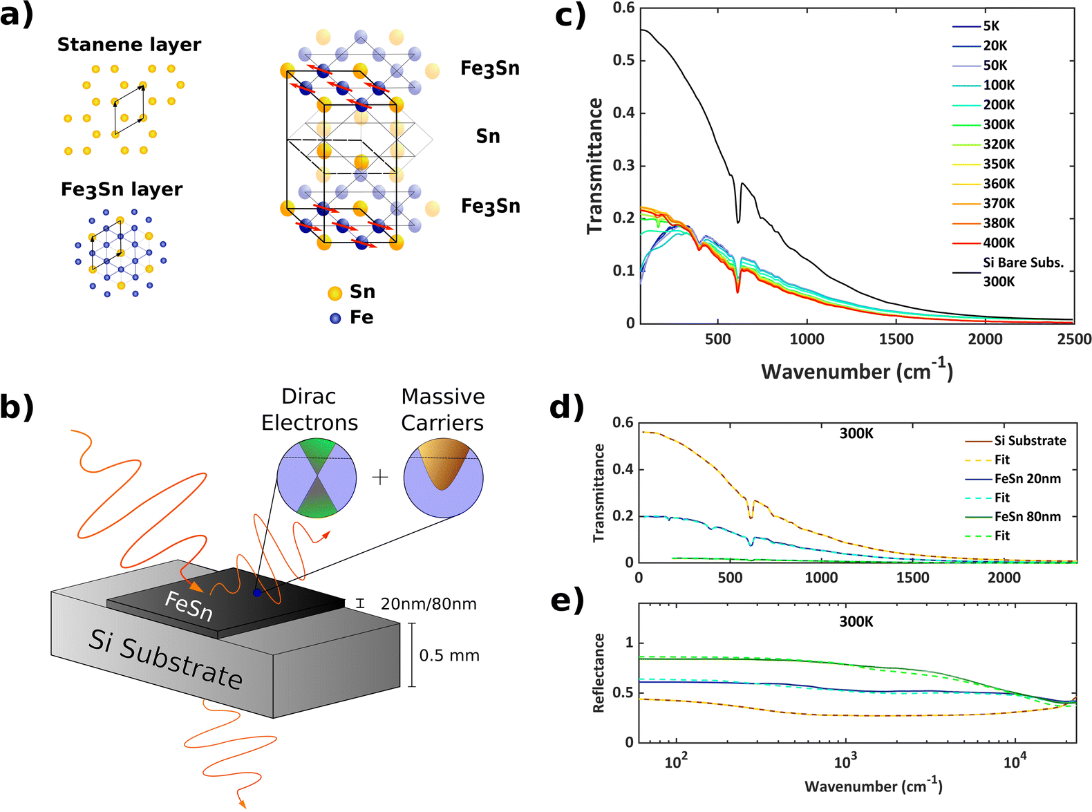 | ||
| Fig. 1 Optical spectroscopy on FeSn thin films. (a) View of the crystal structure and its constituent two-dimensional layers. The kagome lattice of Fe atoms, with Sn atoms in the center of the hexagons, is alternated with a stanene layer within the single unit cell (solid lines). Red arrows indicate the antiferromagnetic exchange between adjacent kagome planes. (b) Schematic representation of the thin film deposited on a Si substrate. When investigating its electrodynamics by means of optical spectroscopy, both Dirac and massive electrons participate in the metallic transport (see main text). (c) Experimental transmittance of bare Si substrate at 300 K and FeSn 20 nm thin film transmittance over a wide temperature range. (d and e) Transmittance and reflectance for all samples at room temperature together with the corresponding Drude–Lorentz fitting required for the extrapolation of FeSn linear response functions. Unlike the other samples, the transmittance of the FeSn 80 nm thin film is reported down to 200 cm−1 due to the low signal-to-noise ratio below that frequency. | ||
In the optical spectroscopy measurements, both transmittance (T) and reflectance (R) spectra were collected. The experimental set-ups are described in the Methods section, while the general technique is shown schematically in Fig. 1b. Transmittance data, obtained for different temperatures, are reported in Fig. 1c for the 20 nm sample together with the transmittance of the bare substrate measured at room temperature. The low-energy transmittance for the film-substrate structure shows a clear drop with decreasing temperature which is related to a rapid increase of FeSn metallicity (see below for further details).
The optical linear response functions of FeSn were obtained through a simultaneous Drude–Lorentz model fit of both R and T using a multilayer model analysis with RefFit software.38Fig. 1(d and e) show the fits performed at room temperature on the different samples. For all the remaining temperatures the procedures are the same and the quality of the fits remains similar. The analysis of Si is crucial since from the determination of its complex refractive index n + ik (see Methods) it is possible to build a Drude–Lorentz model for FeSn, independent of the properties of the substrate, from which the dielectric function and optical conductivity of the kagome metal can be derived.
Fig. 2a shows the real part of the optical conductivity σ1(ω) of the 20 nm FeSn thin film for each temperature from 5 K to 400 K in a spectral range up to 25000 cm−1. Similar results are obtained for the 80 nm film (see the ESI, Sec. I†), whose σ1(ω,T) shows a high compatibility with the optical data found on single crystals.36 Above room temperature the conductivity is scarcely temperature-dependent, showing a nearly flat metallic term (Fig. 2a) and several absorption bands from mid-IR to the VIS range. Below room temperature, σ1(ω) exhibits a strong variation in the low frequency range where a gradual redshift of the metallic spectral weight is progressively observed upon cooling resulting in a significant enhancement of the electronic transport. By extrapolating the optical conductivity at zero frequency, it is possible to obtain the temperature variation of the corresponding zero-frequency optical resistivity ρ = 1/σ1(ω = 0), which is shown in the inset of Fig. 2a (red points). ρ agrees very well with experimental DC resistivity measurement performed on a FeSn thin film deposited on the STO substrate with a thickness of ∼25 nm.43 Moreover, ρ shows a broad kink around the Néel temperature with a maximum at T = 360 K, matching with the barely visible kink present in the DC resistivity data around the same temperature.43 The presence of this kink could be determined by the enhanced spin-scattering associated with the theoretically predicted strong spin fluctuation,31 which can greatly affect transport properties near TN.44
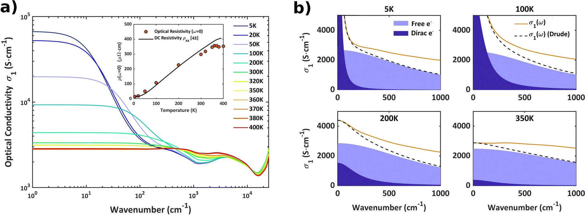 | ||
| Fig. 2 Temperature dependence of the optical conductivity for the FeSn 20 nm thin film. (a) Real part of the optical conductivity σ1(ω) at different temperatures. Above 350 K the temperature dependence is almost absent, providing very small variations over the entire spectrum. The inset shows resistivity data extrapolated from σ1(ω) and calculated at ω = 0 and compared with DC resistivity data (solid black line) of FeSn thin films deposited on the STO43 substrate. (b) Behaviour of the two Drude peaks (see main text) for four representative temperatures: 5, 100, 200 and 350 K. The Drude peak associated with massive free electrons (lighter blue) is weakly temperature-dependent. The Drude peak associated with Dirac electrons (darker blue), by contrast, broadens very rapidly with increasing temperature in conjunction with a progressive decrease in its amplitude. The red solid line corresponds to the full σ1(ω) data while the black dashed lines include only the full Drude contribution to the conductivity. | ||
In order to quantitatively study the temperature dependence of the low energy optical conductivity, a deeper insight needs to be provided on the Drude Lorentz fits performed on the optical data at all temperatures. Satisfactory fits for all the T and R (as the one in Fig. 1d and e) can be obtained by employing the so-called two-carrier model for the low-energy electrodynamics, in which two Drude terms are exploited to fully describe the low energy intra-band transitions. This multichannel charge-carrier dynamics is fully consistent with multiband Hall and Seebeck data on different FeSn samples,31,37,43 and it is further supported by previous optical spectroscopy analysis on Weyl semimetals (WSMs).45–49 Furthermore, Fig. 2b provides a physical interpretation for these two Drude terms. On examining their evolution as temperature increases at 5, 100, 200, and 350 K, it is possible to observe that the peak in lighter blue turns out to be weakly temperature dependent, with small relative variations on the plasma frequency ωp and scattering rate γ (see Fig. 3 for the Drude parameter values). Its plasma frequency increases slightly with increasing temperature as indicated by the behaviour of the spectral weight in Fig. 3a (brown circles), and so does γ (Fig. 3c), as expected for conduction electrons. By contrast, the second Drude peak in Fig. 2b (darker blue) changes very rapidly with temperature. Indeed, its scattering rate γ drops sharply with decreasing temperature reaching the very low value of γ = 13 cm−1 at 5 K, as shown in Fig. 3b. This value is indicative of very high mobilities, characteristic of massless electrons in linearly dispersive bands, and is comparable with γ values characteristic of Dirac electrons in WSMs48–51 and other kagome metals.22,52 This result allows establishing a classification for the two Drude peaks: the former (lighter blue) can be associated with the transport of massive free electrons that populate parabolic dispersive bands while the latter (darker blue) can be associated with highly mobile Dirac fermions.20,27 It is important to note that the same analysis has been carried out in the 80 nm film, showing analogous results in terms of multiband transport channels with the same classification for the electron dynamics (see the ESI†). Thus, the results highlighted in this paper are independent of the film thickness, allowing for the generalization to bulk systems.
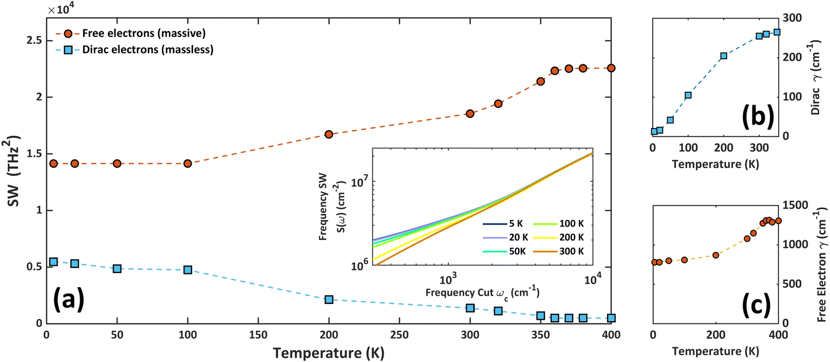 | ||
| Fig. 3 Spectral weight SW and scattering rate γ for the FeSn 20 nm thin film. (a) Temperature dependence of the Drude spectral weight for the two transport channels (see main text). Brown circles describe massive free electrons while blue squares are associated with Dirac electrons. The inset shows the frequency spectral weight calculated on the entire optical conductivity for temperatures up to 300 K. The convergence of the data above ωc = 4000 cm−1 (frequency cut) indicates an almost constant spectral weight up to room temperature. (b and c) Temperature dependence of the scattering rate calculated for both Dirac and massive electrons. Dirac γ(T) is defined up to 350 K due to the negligible contribution of Dirac electrons to spectral weight above that temperature. | ||
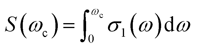
To further develop the above considerations, and to understand the relative importance of the two Drude contributions to the overall electronic transport of the system, we consider their spectral weight (Fig. 3a) calculated as SW = ωp,D2/8 (see ref. 53), where ωp,D is the plasma frequency of each single Drude peak. Up to 100 K the SW remains almost constant for both channels. This means that the change in conductivity at low frequencies is completely driven by the increase in mobility of Dirac electrons, which in turn dominate the DC transport. Above 100 K there is a redistribution of spectral weight from the Drude response of the relativistic fermions toward that of the massive conduction electrons, which constitute the main transport channel already at room temperature. This spectral weight transfer, however, is not perfectly balanced. In fact, the frequency spectral weight S(ωc) shown in the inset of Fig. 3a (with ωc cut-off frequency) and calculated over the entire conductivity as
The variable contribution to transport by Dirac electrons can be explained in terms of the strong scattering rate temperature dependence associated with the massless electron transport channel. The rapid increase of γ(T) for increasing temperatures can be attributed to a strong e–ph coupling interaction, which has been reported on single crystal samples by means of thermal conductivity measurements.31
Related to that, the SW transfer above 100 K could be mainly associated with phonon-mediated inter-band scattering mechanisms, which simply determine a progressive homogenization of electron transport into a single conventional metallic channel. This observation is further supported by the fact that the phonon DOS, which has been determined both theoretically54 and experimentally through neutron scattering measurements,42 exhibits an onset at the energy of ∼10 meV (∼100 K), that is the energy needed to excite long wavevector phonons, which in turn are the ones required for the inter-band scattering processes.
Another important mechanism that could contribute to the increased Dirac scattering rate while approaching TN is a possible shifting of Dirac cones as temperature changes. The antiferromagnetic nature of FeSn is responsible for the exchange splitting of the electronic bands, which simultaneously results in the departure of the flat bands from the Fermi energy together with the shifting of the Dirac point up to ∼−0.4 eV at magnetic saturation.20,36,55,56 Since the magnetization of FeSn gradually builds up as the temperature decreases,31 the settling of the Dirac cones to the ground state band configuration can lead to slight variations in the carrier density and in the effective mass for Dirac electrons, possibly contributing to the behaviour observed in Fig. 3(a and b).
Finally, as the temperature increases above 300 K, no further relevant changes can be observed in the total optical response for any of the two films. In addition to an almost temperature-independent contribution on low-energy electrodynamics, as evident from the conductivity in Fig. 2a (see the ESI† for the 80 nm film), also the interband contributions remain almost invariant up to 400 K, even above the Néel temperature. These results are particularly interesting since the magnetic ordering and the associated symmetries can have non-trivial consequences on the topology and the band structure of the system, thus affecting the electronic transport and transitions as indicated above.
Fig. 4 highlights the interband contributions to the linear response of FeSn (the Drude components have been subtracted) by showing the comparison at room temperature between the real and the imaginary parts of the experimental dielectric function ε(ω) = ε1(ω) + iε2(ω) with the one calculated numerically by means of DFT (see Methods section) for the bulk system. The good correspondence with the experimental data, especially for the case of the 80 nm film which is closer to the realization of a bulk crystalline structure, suggests the good quality of the fits calculated for the optical data.
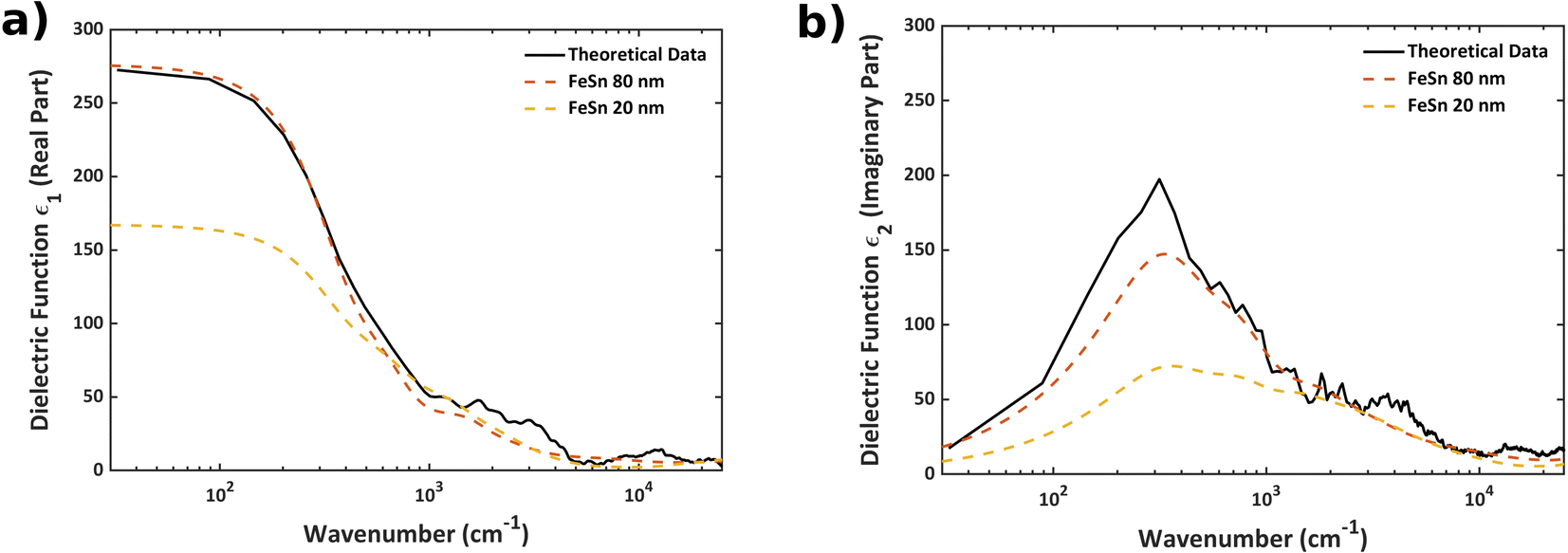 | ||
| Fig. 4 Analysis of the interband contribution to the linear response of both FeSn thin films. Comparison of the real (a) and imaginary (b) parts of the dielectric function ε(ω) = ε1(ω) + iε2(ω) obtained from the optical data in Fig. 1(d and e) for both the FeSn samples with the bulk dielectric function calculated theoretically. Both the Drude oscillators have been completely removed from all the models in order to highlight the interband contribution to the linear response of the system. The emergent low energy absorption peak around 400 cm−1 in the imaginary part of the dielectric function (b) is associated with electronic transitions between bands close to the Fermi energy along the Γ → K direction in the Brillouin zone. Its contribution to the measured optical conductivities is mainly hidden by the Drude terms (see main text). | ||
In order to gain a deeper insight on the inter-band electronic transitions, and to verify the possible emergence of spectral features related to transitions between the exotic electronic states that characterize the kagome metals such as FeSn, it is particularly useful to investigate the properties of the imaginary part of the dielectric function shown in Fig. 4b. The most obvious signature, which appears as an absorption peak in the spectral region between 100 cm−1 and 1000 cm−1, which correspond to an absorption edge in the real part of the optical conductivity σ1(ω), is attributed to the onset of low-energy electronic transitions around the Fermi energy along the Γ → K direction in the Brillouin zone. It is interesting to note that this spectral feature cannot be associated with transitions from the flat bands since they are identified in the optical conductivity σ1 of other kagome systems as very narrow asymmetric peaks,22,26 which are not observed in this case. Moreover, the flat bands observed experimentally for FeSn (ref. 20 and 29) are ∼0.25 eV below the Fermi energy, suggesting the appearance of an absorption peak at slightly higher frequencies. Furthermore, it is not possible to attribute the present spectral feature to electronic transitions between Dirac cones because the corresponding Pauli absorption edge should lie in the spectrum at energy values that are twice the Dirac point energy ED ∼ −0.4 eV (ref. 26) (thus at ∼6500 cm−1). Finally, it is interesting to note that the occurrence of this spectral feature is not apparent in the full linear response of the system (Fig. 2a) due to the fact that the Drude contributions merge with the onset of the electronic transitions. Nonetheless, based on the numerical results obtained in Fig. 4b, the absorption peak is included in the Drude–Lorentz model for the optical fit to the experimental data through the introduction of two oscillators centered at the resonance frequencies ω0 ∼ 390 cm−1 and ω0 ∼ 800 cm−1 (see the ESI†).
The other two visible absorption peaks that appear both in ε2(ω) and σ1(ω) around 4000 cm−1 (0.5 eV) and 14000 cm−1 (1.7 eV) are instead associated with vertical transitions over the entire Brillouin zone between the many electronic band states that characterize the FeSn band structure. It is important to emphasize that no distinct features ascribed to the fingerprints of kagome systems can be identified in the optical inter-band response of the system. In particular, the transitions between Dirac states, that introduce a distinct linear or constant-frequency dependence in the conductivity depending on the dimensionality of the Dirac cones,49 cannot be identified in the broad absorption contribution provided by the several inter-band transitions characterizing the system. This result is consistent with the observations proposed in the recent study on FeSn optical anisotropy.36
Conclusions
In this work, we investigated the electrodynamics of the novel antiferromagnetic kagome metal FeSn by means of optical spectroscopy over a wide frequency range from THz to visible. Through the analysis of the Drude contribution to the optical conductivity we demonstrated the presence of two electronic transport channels associated in one case with massive conventional charge carriers and in the other with massless relativistic fermions populating linear dispersive Dirac states. The latter in particular stands out in overall transport due to the high mobility values enhanced by the suppression of e–ph scattering as temperature decreases. Furthermore, the dielectric functions obtained from the experimental data were compared with the DFT theoretical calculation obtained for the bulk. The compatibility of the results provides a validation of the models used to analyze the system.Finally, all those results were obtained for FeSn thin films deposited on a Si substrate. Such a configuration is especially promising as it opens the way towards the realisation of technological devices suitable for electronics and spintronics applications, exploiting in particular the tremendous potential arising from the interplay between magnetism and topology.
Data availability
The original contributions presented in the study are included in the article and ESI,† further inquiries can be directed to the corresponding author.Author contributions
Experimental design: Salvatore Macis and Stefano Lupi. Materials: Niraj Bhattarai and John Philip. Methodology: Lorenzo Mosesso, Luca Tomarchio, Salvatore Macis, Antonio Grilli, Mariangela Cestelli Guidi. Data curation: Lorenzo Mosesso and Luca Tomarchio. Formal analysis: Lorenzo Mosesso and Luca Tomarchio. Software: Olivia Pulci and Paola Gori. Original draft preparation: Lorenzo Mosesso and Stefano Lupi. All authors reviewed the manuscript. All authors have read and agreed with the published version of the manuscript.Conflicts of interest
There are no conflicts to declare.Acknowledgements
We acknowledge the Ministero dell'Università e della Ricerca (MUR), call PRIN 2020, project “PHOtonics Terahertz devices based on topological materials” (“PHOTO”), grant no. 2020RPEPNH. CPU time was granted by CINECA HPC center. This publication was supported by the European Union (EU) under the Italian National Recovery and Resilience Plan (NRRP) of Next Generation EU partnership PE0000023-NQSTI.Notes and references
- H.-M. Guo and M. Franz, Phys. Rev. B: Condens. Matter Mater. Phys., 2009, 80, 113102 CrossRef.
- I. I. Mazin, H. O. Jeschke, F. Lechermann, H. Lee, M. Fink, R. Thomale and R. Valentí, Nat. Commun., 2014, 5, 4261 CrossRef CAS.
- L. Balents, Nature, 2010, 464, 199–208 CrossRef CAS.
- L. Savary and L. Balents, Rep. Prog. Phys., 2016, 80, 016502 CrossRef PubMed.
- H. Chen, Q. Niu and A. H. MacDonald, Phys. Rev. Lett., 2014, 112, 017205 CrossRef PubMed.
- J. Kübler and C. Felser, Europhys. Lett., 2014, 108, 67001 CrossRef.
- N. Chowdhury, K. I. A. Khan, H. Bangar, P. Gupta, R. S. Yadav, R. Agarwal, A. Kumar and P. K. Muduli, Proc. Natl. Acad. Sci. India Sect. A (Phys. Sci.), 2023, 93, 477–495 CrossRef.
- S. Nakatsuji, N. Kiyohara and T. Higo, Nature, 2015, 527, 212–215 CrossRef CAS.
- A. K. Nayak, J. E. Fischer, Y. Sun, B. Yan, J. Karel, A. C. Komarek, C. Shekhar, N. Kumar, W. Schnelle, J. Kübler, C. Felser and S. S. P. Parkin, Sci. Adv., 2016, 2, e1501870 CrossRef.
- K. Kuroda, T. Tomita, M.-T. Suzuki, C. Bareille, A. A. Nugroho, P. Goswami, M. Ochi, M. Ikhlas, M. Nakayama, S. Akebi, R. Noguchi, R. Ishii, N. Inami, K. Ono, H. Kumigashira, A. Varykhalov, T. Muro, T. Koretsune, R. Arita, S. Shin, T. Kondo and S. Nakatsuji, Nat. Mater., 2017, 16, 1090–1095 CrossRef CAS PubMed.
- H. Zhang, H. Feng, X. Xu, W. Hao and Y. Du, Adv. Quantum Technol., 2021, 4, 2100073 CrossRef CAS.
- A. Bolens and N. Nagaosa, Phys. Rev. B, 2019, 99, 165141 CrossRef CAS.
- K. Sun, Z. Gu, H. Katsura and S. Das Sarma, Phys. Rev. Lett., 2011, 106, 236803 CrossRef PubMed.
- P. Di Pietro, M. Ortolani, O. Limaj, A. Di Gaspare, V. Giliberti, F. Giorgianni, M. Brahlek, N. Bansal, N. Koirala, S. Oh, P. Calvani and S. Lupi, Nat. Nanotechnol., 2013, 8, 556–560 CrossRef CAS PubMed.
- F. Giorgianni, E. Chiadroni, A. Rovere, M. Cestelli-Guidi, A. Perucchi, M. Bellaveglia, M. Castellano, D. Di Giovenale, G. Di Pirro, M. Ferrario, R. Pompili, C. Vaccarezza, F. Villa, A. Cianchi, A. Mostacci, M. Petrarca, M. Brahlek, N. Koirala, S. Oh and S. Lupi, Nat. Commun., 2016, 7, 11421 CrossRef CAS.
- L. Tomarchio, L. Mosesso, S. Macis, A. Grilli, M. Romani, M. C. Guidi, K. Zhu, X. Feng, M. Zacchigna, M. Petrarca, K. He and S. Lupi, NPG Asia Mater., 2022, 14, 1–7 CrossRef.
- L. Tomarchio, S. Mou, L. Mosesso, A. Markou, E. Lesne, C. Felser and S. Lupi, ACS Appl. Electron. Mater., 2023, 5, 1437–1443 CrossRef CAS.
- C. Grazianetti, S. De Rosa, C. Martella, P. Targa, D. Codegoni, P. Gori, O. Pulci, A. Molle and S. Lupi, Nano Lett., 2018, 18, 7124–7132 CrossRef CAS.
- S. Macis, A. D'Arco, L. Mosesso, M. C. Paolozzi, S. Tofani, L. Tomarchio, P. P. Tummala, S. Ghomi, V. Stopponi, E. Bonaventura, C. Massetti, D. Codegoni, A. Serafini, P. Targa, M. Zacchigna, A. Lamperti, C. Martella, A. Molle and S. Lupi, Adv. Mater., 2024, 36, 2400554 CrossRef CAS.
- M. Kang, L. Ye, S. Fang, J.-S. You, A. Levitan, M. Han, J. I. Facio, C. Jozwiak, A. Bostwick, E. Rotenberg, M. K. Chan, R. D. McDonald, D. Graf, K. Kaznatcheev, E. Vescovo, D. C. Bell, E. Kaxiras, J. van den Brink, M. Richter, M. Prasad Ghimire, J. G. Checkelsky and R. Comin, Nat. Mater., 2020, 19, 163–169 CrossRef CAS.
- Q. Wang, Y. Xu, R. Lou, Z. Liu, M. Li, Y. Huang, D. Shen, H. Weng, S. Wang and H. Lei, Nat. Commun., 2018, 9, 3681 CrossRef.
- Y. Xu, J. Zhao, C. Yi, Q. Wang, Q. Yin, Y. Wang, X. Hu, L. Wang, E. Liu, G. Xu, L. Lu, A. A. Soluyanov, H. Lei, Y. Shi, J. Luo and Z.-G. Chen, Nat. Commun., 2020, 11, 3985 CrossRef CAS PubMed.
- M. Kang, S. Fang, L. Ye, H. C. Po, J. Denlinger, C. Jozwiak, A. Bostwick, E. Rotenberg, E. Kaxiras, J. G. Checkelsky and R. Comin, Nat. Commun., 2020, 11, 4004 CrossRef CAS PubMed.
- L. Ye, M. Kang, J. Liu, F. von Cube, C. R. Wicker, T. Suzuki, C. Jozwiak, A. Bostwick, E. Rotenberg, D. C. Bell, L. Fu, R. Comin and J. G. Checkelsky, Nature, 2018, 555, 638–642 Search PubMed.
- Z. Lin, J.-H. Choi, Q. Zhang, W. Qin, S. Yi, P. Wang, L. Li, Y. Wang, H. Zhang, Z. Sun, L. Wei, S. Zhang, T. Guo, Q. Lu, J.-H. Cho, C. Zeng and Z. Zhang, Phys. Rev. Lett., 2018, 121, 096401 CrossRef PubMed.
- A. Biswas, O. Iakutkina, Q. Wang, H. C. Lei, M. Dressel and E. Uykur, Phys. Rev. Lett., 2020, 125, 076403 CrossRef CAS.
- Z. Lin, C. Wang, P. Wang, S. Yi, L. Li, Q. Zhang, Y. Wang, Z. Wang, H. Huang, Y. Sun, Y. Huang, D. Shen, D. Feng, Z. Sun, J.-H. Cho, C. Zeng and Z. Zhang, Phys. Rev. B, 2020, 102, 155103 CrossRef CAS.
- M. Han, H. Inoue, S. Fang, C. John, L. Ye, M. K. Chan, D. Graf, T. Suzuki, M. P. Ghimire, W. J. Cho, E. Kaxiras and J. G. Checkelsky, Nat. Commun., 2021, 12, 5345 CrossRef CAS PubMed.
- D. Multer, J.-X. Yin, M. S. Hossain, X. Yang, B. C. Sales, H. Miao, W. R. Meier, Y.-X. Jiang, Y. Xie, P. Dai, J. Liu, H. Deng, H. Lei, B. Lian and M. Zahid Hasan, Commun. Mater., 2023, 4, 1–6 CrossRef.
- H. Giefers and M. Nicol, J. Alloys Compd., 2006, 422, 132–144 CrossRef CAS.
- B. C. Sales, J. Yan, W. R. Meier, A. D. Christianson, S. Okamoto and M. A. McGuire, Phys. Rev. Mater., 2019, 3, 114203 CrossRef CAS.
- M. Kakihana, K. Nishimura, D. Aoki, A. Nakamura, M. Nakashima, Y. Amako, T. Takeuchi, T. Kida, T. Tahara, M. Hagiwara, H. Harima, M. Hedo, T. Nakama and Y. Ōnuki, J. Phys. Soc. Jpn., 2019, 88, 014705 CrossRef.
- B. C. Sales, B. Saparov, M. A. McGuire, D. J. Singh and D. S. Parker, Sci. Rep., 2014, 4, 7024 Search PubMed.
- E. Uykur, B. R. Ortiz, O. Iakutkina, M. Wenzel, S. D. Wilson, M. Dressel and A. A. Tsirlin, Phys. Rev. B, 2021, 104, 045130 CrossRef CAS.
- E. Uykur, B. R. Ortiz, S. D. Wilson, M. Dressel and A. A. Tsirlin, npj Quantum Mater., 2022, 7, 1–8 CrossRef.
- J. Ebad-Allah, M.-C. Jiang, R. Borkenhagen, F. Meggle, L. Prodan, V. Tsurkan, F. Schilberth, G.-Y. Guo, R. Arita, I. Kézsmárki and C. A. Kuntscher, Phys. Rev. B, 2024, 109, L201106 Search PubMed.
- N. Bhattarai, A. W. Forbes, R. S. H. Saqat, I. L. Pegg and J. Philip, Phys. Status Solidi A, 2023, 220, 2200677 CrossRef CAS.
- A. B. Kuzmenko, Rev. Sci. Instrum., 2005, 76, 083108 CrossRef.
- P. Giannozzi, S. Baroni, N. Bonini, M. Calandra, R. Car, C. Cavazzoni, D. Ceresoli, G. L. Chiarotti, M. Cococcioni, I. Dabo, A. D. Corso, S. de Gironcoli, S. Fabris, G. Fratesi, R. Gebauer, U. Gerstmann, C. Gougoussis, A. Kokalj, M. Lazzeri, L. Martin-Samos, N. Marzari, F. Mauri, R. Mazzarello, S. Paolini, A. Pasquarello, L. Paulatto, C. Sbraccia, S. Scandolo, G. Sclauzero, A. P. Seitsonen, A. Smogunov, P. Umari and R. M. Wentzcovitch, J. Phys.: Condens. Matter, 2009, 21, 395502 CrossRef PubMed.
- J. P. Perdew, K. Burke and M. Ernzerhof, Phys. Rev. Lett., 1996, 77, 3865–3868 CrossRef CAS PubMed.
- H. J. Monkhorst and J. D. Pack, Phys. Rev. B: Solid State, 1976, 13, 5188–5192 CrossRef.
- Y. Tao, L. Daemen, Y. Cheng, J. C. Neuefeind and D. Louca, Phys. Rev. B, 2023, 107, 174407 CrossRef CAS.
- H. Inoue, M. Han, L. Ye, T. Suzuki and J. G. Checkelsky, Appl. Phys. Lett., 2019, 115, 072403 Search PubMed.
- J. Cui, M. Shi, H. Wang, F. Yu, T. Wu, X. Luo, J. Ying and X. Chen, Phys. Rev. B, 2019, 99, 155125 CrossRef CAS.
- C. C. Homes, M. N. Ali and R. J. Cava, Phys. Rev. B: Condens. Matter Mater. Phys., 2015, 92, 161109 CrossRef.
- D. Neubauer, A. Yaresko, W. Li, A. Löhle, R. Hübner, M. B. Schilling, C. Shekhar, C. Felser, M. Dressel and A. V. Pronin, Phys. Rev. B, 2018, 98, 195203 CrossRef CAS.
- M. B. Schilling, A. Löhle, D. Neubauer, C. Shekhar, C. Felser, M. Dressel and A. V. Pronin, Phys. Rev. B, 2017, 95, 155201 CrossRef.
- S. Kimura, Y. Nakajima, Z. Mita, R. Jha, R. Higashinaka, T. D. Matsuda and Y. Aoki, Phys. Rev. B, 2019, 99, 195203 CrossRef CAS.
- Z.-Y. Qiu, Z.-Y. Liao and X.-G. Qiu, Chin. Phys. B, 2019, 28, 047801 CrossRef CAS.
- H. J. Park, B. C. Park, M.-C. Lee, D. W. Jeong, J. Park, J. S. Kim, H. S. Ji, J. H. Shim, K. W. Kim, S. J. Moon, H.-D. Kim, D.-Y. Cho and T. W. Noh, Phys. Rev. B, 2017, 96, 155139 CrossRef.
- B. Xu, Y. M. Dai, L. X. Zhao, K. Wang, R. Yang, W. Zhang, J. Y. Liu, H. Xiao, G. F. Chen, A. J. Taylor, D. A. Yarotski, R. P. Prasankumar and X. G. Qiu, Phys. Rev. B, 2016, 93, 121110 CrossRef.
- R. Yang, T. Zhang, L. Zhou, Y. Dai, Z. Liao, H. Weng and X. Qiu, Phys. Rev. Lett., 2020, 124, 077403 CrossRef CAS PubMed.
- M. Dressel and G. Grüner, Electrodynamics of Solids, Cambridge University Press, 2002 Search PubMed.
- A. Ptok, A. Kobiałka, M. Sternik, J. Łażewski, P. T. Jochym, A. M. Oleś, S. Stankov and P. Piekarz, Phys. Rev. B, 2021, 104, 054305 CrossRef CAS.
- Y. Xie, L. Chen, T. Chen, Q. Wang, Q. Yin, J. R. Stewart, M. B. Stone, L. L. Daemen, E. Feng, H. Cao, H. Lei, Z. Yin, A. H. MacDonald and P. Dai, Commun. Phys., 2021, 4, 1–11 CrossRef.
- R. G. Moore, S. Okamoto, H. Li, W. R. Meier, H. Miao, H. N. Lee, M. Hashimoto, D. Lu, E. Dagotto, M. A. McGuire and B. C. Sales, Phys. Rev. B, 2022, 106, 115141 Search PubMed.
Footnote |
| † Electronic supplementary information (ESI) available. See DOI: https://doi.org/10.1039/d4na00737a |
| This journal is © The Royal Society of Chemistry 2024 |